Note: Descriptions are shown in the official language in which they were submitted.
HE179-70077CIP
SYSTEM FOR PROVIDING POWER AND DATA TRANSMISSION
BETWEEN A DOOR AND A FRAME
TECHNICAL FIELD
The present invention relates to systems for providing electric
power/communication between a first object and a second object; more
particularly, to such a system wherein said first and second objects are not
physically connected electrically; and most particularly, to such a system
wherein
components and circuitry enable such power/communication at a Baud rate of
essentially twice the frequency of the voltage being transferred between the
first
and second objects or, in a second embodiment, voltage transfer is at 20 KHz
and
data transfer is in the range of 100K baud. Further embodiments include
compact
packaging of the components and utilize fiber optic cables to enable
communication between the first object and the second object.
BACKGROUND OF THE INVENTION
It is known in the art of security and electrically-controlled locks to use
keypads and other input devices to provide secure access to buildings or other
objects, e.g. safes, automobiles, and the like. In conjunction with this
trend, a
need has also developed for transmission of various types of functions or
information relating to a door secured in a frame. For example, it can be
1
CA 2792041 2017-10-11
CA 02792041 2012-10-11
desirable in a security application to provide power across a frame-door gap
to
the region around a lock in order to energize an actuator, solenoid, motor,
etc, or
to recharge a battery used in engaging/disengaging the lock, or power an
identification device located on the door. It can also be desirable to
determine
the status or lock-state of the lock, i.e., whether the locking mechanism is
engaged or disengaged or whether a door is open or closed. This status
information must in some way be acquired and transmitted across the door-frame
gap to a monitoring device such as a computer controller.
Prior art systems transfer power and/or data between a door and a door
frame using wires that run through a mechanical hinge point or a set of spring
loaded contacts that provide an electrical connection across the frame-door
gap
when the door is in the closed position. The problem with such a wire-based
approach is that only very fine wires can be used since such wires must pass
internally through the plates of the door hinges to avoid being severed in
normal
operation or by an intruder. Spring-loaded contacts present a different set of
problems relating to contamination of the contacts and the risk of shocking a
person passing through the door who might make contact with the 'live' contact
set on the frame.
What is needed in the art is a robust and efficient system that provides
wire-free power transfer between a frame and a door and also enables
information or communication transfer, all the while avoiding the above
shortcomings of prior art systems.
What is further needed in the art is a compact system that minimizes the
area in the door that is taken up by the device or which can utilize the space
already provided for a dead bolt, within a mortise lockset, for the compact
system.
What is yet further needed in the art is a system wherein its circuitry
optimizes power output of the device.
It is a principal object of the present invention to provide a compact, wire-
free communications and power transmission system between a door and a
frame.
( 1551611:
2
CA 02792041 2012-10-11
SUMMARY OF THE INVENTION
Briefly described, the present invention provides transfer of power and/or
data from a first object to a second object, such as a frame to a door,
utilizing a
split core transformer wherein portions of the core and windings are located
in
both the door and the frame. Status and data may be transmitted between a
device located in the door and a device in the frame at data rates that are
essentially twice the frequency of the voltage applied to the primary side of
the
split core transformer or up to 100kHz in an alternate embodiment. In a
further
embodiment, status and data may be transmitted and received through use of
fiber optic cables.
A door and frame equipped with a split core transformer in accordance with
one aspect of the present invention comprise mating halves or portions of the
transformer that provides wire-free and contact-free power transfer between
the
frame and the door and also enables information or communication transfer. The
door frame comprises a subassembly of the split core transformer having a
recessed portion housing a first transformer core portion having first
windings.
The associated door is provided with a spring-loaded subassembly of the split
core transformer having a protruding portion fitted with a second transformer
core
portion having second windings, When the door is closed against the frame, the
recessed portion in the frame is formed to receive the spring-loaded
protruding
portion of the door whereby the first and second core portions are aligned and
brought into such close proximity as to minimize the air-gap between the
cores,
allowing transfer of power/data via magnetic induction from one transformer
portion to the other. Such power/data may flow bi-directionally from either of
the
transformers halves to the other.
Power may be provided across the frame/door gap to energize a solenoid
or other powered actuator for locking the door or to recharge a battery
located in
an identification device, such as an electronic combination locking device on
the
door. Preferably, a sensing winding is provided adjacent the primary winding
of
( 1551811 : 1
3
CA 02792041 2012-10-11
the first portion of the split core transformer to capture modulated
alternating
current from the secondary winding that is located in the second portion of
the
split core transformer.
In a further embodiment of the split core transformer, a door and a frame
are equipped with mating transformer core portions that also provide wire-free
and contact-free power and data transfer between the frame and the door. In
one particular aspect of the further embodiment, the mating transformer core
portions may be compact, pot core portions. In a first example of the further
embodiment, the door frame includes a housing equipped with a first
transformer
core portion having first windings, while the associated door is provided with
a
spring-loaded protruding assembly fitted with a second transformer core
portion
having second windings. When the door is closed against the frame, the spring-
loaded assembly aligns and brings the first and second transformer core
portions
within such close proximity so as to minimize the air-gap between the
portions,
thereby allowing transfer of power via magnetic induction from one transformer
core portion to the other. Each transformer core portion may further be
equipped
with a fiber optic cable composed of numerous individually-clad fibers
arranged
coaxially so as to permit two-way communication between the frame and the
door.
In a second example of the further embodiment, fixed transformer core
portions approximately 1 inch in width are matingly fitted in a door and a
door
frame resulting in a varying gap between the transformer core portions, from
one
door/frame unit to the next, when the door is closed. Paired resonating
circuits of
the fixed transformer core portion are off-tuned so as to yield a more
constant
output level over a varying gap. In the second example, each transformer core
portion may also be equipped with a fiber optic cable composed of numerous
individually-clad fibers arranged coaxially so as to permit two-way
communication
between the frame and the door.
Additional benefits of the above described system and method for providing
power and data communication respecting a door and lock are set forth in the
following discussion.
( 1551811 : )
4
CA 02792041 2012-10-11
BRIEF DESCRIPTION OF THE DRAWINGS
The present invention will now be described, by way of example, with
reference to the accompanying drawings, in which:
FIG. 1 is an exploded isometric drawing of a spring-loaded protruding
subassembly in accordance with the present invention including a second
transformer core portion;
FIG. 2 is an exploded isometric drawing in accordance with the present
invention comprising the subassembly shown in FIG. 1;
FIG. 3 is an isometric drawing showing the subassembly shown in FIG. 2
mounted in a second object such as a door;
FIG. 4 is an exploded isometric drawing of a mating subassembly of the
subassembly shown in FIGS. 1-3, in accordance with the present invention,
comprising a first transformer core portion;
FIG. 5 is an isometric drawing showing the subassembly shown in FIG. 4
mounted in a first object such as a mating frame;
FIG. 6 is a first elevational cross-sectional view of a system for providing
power and data transmission in accordance with the present invention, taken
through the center of the two subassemblies and showing the subassembly
shown in FIGS. 1-3 engaged but not yet nested with the subassembly shown in
FIGS. 4 and 5;
FIG. 7 is a sequential elevational cross-sectional view to that shown in
FIG. 6, showing one subassembly engaged and nested with the other
subassembly;
FIG. 8 is a second elevational cross-sectional view taken parallel to the
view shown in FIG. 7, showing the relationship of the cores of the first and
second transformer core portions when the subassemblies are nested together;
FIG. 9 is an isometric view of an exemplary installation in accordance with
the present invention, showing an open door hinged in a frame, the door being
( 1551811 :
CA 02792041 2012-10-11
equipped with a subassembly in accordance with FIGS. 1-3 and the frame being
equipped with a subassembly in accordance with FIGS. 4 and 5;
FIG. 10 is a schematic diagram of an exemplary circuit for implementing
the door side of the present invention;
FIG. 11 is a schematic diagram of an exemplary circuit for implementing
the frame side of the present invention;
FIG. 12 is an exemplary timing sequence of signals and data transmission
between the door and frame in one embodiment of the present invention;
FIG. 13 is a schematic diagram of an alternate embodiment of an
exemplary circuit for implementing the frame side of the present invention to
support bi-directional high speed data communications;
FIG. 14 is a schematic diagram of an exemplary 20KHz sine wave
generator for providing power from the frame sided of FIG 13 in the present
invention;
FIG. 15 is a schematic diagram of an alternate embodiment of an
exemplary circuit for implementing the door side of the present invention to
support bi-directional high speed data communications;
FIG. 16 is a perspective view of a lock body and strike plate of an
additional embodiment of the present invention;
FIG. 17 is an exploded view of the strike plate of the embodiment of FIG.
16;
FIG. 18 is an exploded view of the lock body of the embodiment of FIG.
16;
FIG. 19 is a detailed perspective view of a pair of transformer core
portions with optional fiber optic cables of yet a further embodiment of the
present invention;
FIG. 20 is a side view of a pair of transformer core portions with fiber optic
communication therebetween;
Fig. 21 is a schematic diagram of an exemplary simulation circuit for
implementing the power transmission features of the present invention;
(1551811: )
6
CA 02792041 2012-10-11
Fig_ 22 is a schematic diagram of an exemplary frame side transmitting
circuit;
Fig. 23 is a schematic diagram of an exemplary door side receiving circuit;
Fig. 24 is a graphical representation illustrating the relationship of gap
between system cores and the output voltage as well as the input current for
matched resonance capacitors; and
Fig. 25 is a graphical representation illustrating the relationship of gap
between system cores and the output voltage as well as the input current for
off
tuned resonance capacitors.
Corresponding reference characters indicate corresponding parts
throughout the several views. The exemplification set out herein illustrates
one
preferred embodiment of the invention, in one form, and such exemplification
is
not to be construed as limiting the scope of the invention in any manner.
DESCRIPTION OF THE PREFERRED EMBODIMENTS
In general, the system described herein for providing power and data
transfer in accordance with the present invention may be implemented in a
variety of hardware and software embodiments or combinations thereof.
Referring now to FIGS. 1 through 9, the present invention generally relates
to a system 10 which contains a method for providing power to an entry system
device 12 located on a door 14 hinged in a frame 16 and for providing data
transfer between an entry system device 12 and its mating device 18 on the
frame side of the door through a split core electromagnetic transformer 20
comprising first and second transformer core portions 24, 22 disposed
respectively in frame device 18 and door device 12. The first embodiment
provides circuitry to enable such communication to occur at a Baud rate of
essentially twice the frequency of the voltage being transferred between the
door
and frame side.
The present invention is applicable to doors, windows, or other objects that
are moveable relative to a frame or other fixed object, wherein there is a
need to
{ 1551811 : )
7
CA 02792041 2012-10-11
communicate without direct electrical connection between a device located on
the first object and a device located on the second object. The invention is
described herein with reference to an exemplary environment such as is shown
in FIG. 9, wherein the first object is door 14 and the second object is door
frame
16. As shown, door 14 may have attached thereto an electronic combination
lock 26 or other similar entry system device such as a biometric reader,
magnetic
card reader, and the like. Importantly, such a device, such as electronic
combination lock 26, requires communication with frame 16 and/or a supply of
power from the frame side. Communication between door 14 and frame 16 may
be for the purpose of exchanging information regarding such things as lock
status or the keyed or inputted entry data provided at the lock, or to enable
the
reconfiguration of lock 26 with a new combination. Power to lock 26 may be
required for normal operation or to recharge a battery (not shown) located
therein. As will be appreciated by one skilled in the art, combination lock 26
may
activate a solenoid (not shown), or other similar mechanism for latching,
locking,
opening, or otherwise maintaining the door in a particular position. In the
presently described embodiment, device 12 engages device 18 when the door is
in the closed position.
The system and method for the transfer of power and subsequently for the
communication of data between door 14 and frame 16 may be described with
initial reference to the perspective view of a split transformer 20 having a
first
transformer core portion 24 and second transformer core portion 22, as shown
in
FIGS. 6 through 8. It will be appreciated by one skilled in the art that a
split core
transformer 20 comprises two core halves 22a,24a each having one or more
windings 22b,24b, the two halves being brought together in operation in as
close
a configuration as possible so as to reduce or eliminate any air-gap 28 (FIG.
8)
between the cores halves 22a,24a of each transformer core portion 22,24. The
illustrated second transformer core portion 22 comprises a U-shaped core half
22a having a pair of coil windings 23a,23b located on each leg of core half
22a.
First transformer core portion 24 similarly comprises a U-shaped laminated
core
half 24a and a pair of coil windings 25a,25b.
( 1551811 : I
8
CA 02792041 2012-10-11
Referring now specifically to FIGS. 1 through 3, device 12 comprises a
protruding subassembly 30, an upper housing 32, and a lower housing 34 for
receiving subassembly 30. Protruding subassembly 30 comprises second
transformer core portion 22 as described above received in a well 36 in a
lower
fixture 38 and captured therein by an upper fixture 40 having a ramped portion
42
separating first and second openings 44 for receiving core half 22a. A
compression spring 46 is seated in a spring retainer portion 48 of lower
fixture
38. As received in upper and lower housings 32, 34, spring 46 is compressively
disposed in well 50 in lower housing 34. Upper fixture 40 is slidably disposed
in
upper housing 32 and is urged against end flange 51 by spring 46. During
engagement of device 12, subassembly 30 is free to be displaced axially within
upper housing 32 and upon latching is returned by spring 46 to a predetermined
correct position against flange 50 whereby legs of core half 22a are extended
a
correct distance through openings 44 in upper housing 40.
Referring now to FIGS. 4 and 5, device 18 comprises first transformer core
portion 24 disposed in a well 52 in lower receiver housing 54 and is retained
therein by upper receiver housing 56 having protruding assembly receiver 58
separating first and second openings 60 for receiving legs of core half 24a of
first
transformer 24. Striker plate 62 is secured to upper receiver housing 56 by
screws 64, and device 18 is secured to frame 16 by retainer 66 and screws 68.
Lower and upper receiver housings 54, 56 are formed such that the legs of core
half 24a are extended a correct distance through openings 60 in upper housing
56.
In operation, device 12 and device 18 are located, respectively, in each of
door 14 and frame 16; i.e., device 12 is bore-in installed in the edge of door
14,
and device 18 is recessed into frame 16. First and second transformer core
portions 24,22 are sized and dimensioned to fit within the respective
components
of the frame 16 or door 14. Further, first and second transformer core portion
24,
22 are located so as to be aligned and in close proximity for proper operation
when door 14 is latched into frame 16. That is, first and second transformer
core
portions 24, 22 are positioned one with respect to the other in at least one
( 1551811; )
9
CA 02792041 2012-10-11
position that defines a magnetic circuit, enabling a variable current in
either of
second coil windings 23a, 23b or first coil windings 25a, 25b to induce a
magnetic flux in its respective core half 22a or 24a and thereby inductively
create
an electric current in the other coil 23a, 23b or 25a,25b. Additionally,
device 12
may be housed within door 14 with set screws 19 (FIG. 3), which may also be
utilized to adjust the depth of penetration of the device 12 into door 14.
This
adjustment provides yet another means to minimize the air-gap 28.
In a first embodiment, coil winding 25b is a sense winding designed to
have fewer windings than coil winding 25a of core half 24a. In a second
embodiment, there are windings for power transfer, and transmit and receive,
for
both door and frame.
In a typical installation, first transformer core portion 24, being mounted in
the fixed frame, is connected to an external source of power (not shown) which
produces current and voltage inductively in second transformer core portion 22
mounted in door 14; however, it is obvious that power produced in transformer
core portion 22, as by a battery (BAT1, FIG. 10) disposed in door 14, can
create
current and voltage in transformer core portion 24. Thus, data transfer is
possible in both directions between door 14 and frame 16.
Referring now to FIGS. 6 through 8, in operation, as door 14 closes within
frame 16, protruding ramp 42 engages and rides up the inclined surface of
strike
plate 62 (FIG. 6). Protruding subassembly 30 slides axially within upper and
lower housings 32, 34, compressing spring 46. Further travel in the direction
of
door closing (FIG. 7) allows protruding ramp 42 to be urged by spring 46 into
receiver 58 in device 18, as shown.
When door 14 is in the closed position within the frame 16 device 18 is
adapted and aligned to receive the protruding ramp 42 in a fit and manner as
to
align (FIG. 8) the opposing core halves 24a, 22a of first and second
transformer
core portions 24, 22 and to minimize air gap 28 there between. This closed
door
configuration of the transformer enables the transfer of power and data
between
the door 14 and frame 16 when an alternating current is applied to the frame
side
transformer core portion 24 by utilizing the circuit present in door 14 in
(1551811;
CA 02792041 2012-10-11
cooperation with door transformer core portion 22 and the circuit present in
frame
16.
Note that in all FIGS. 1 through 9, conventional connecting wiring is
assumed and is therefore omitted for clarity.
Referring now to FIGS. 10 through 12, the present invention further
comprises circuitry of components that are utilized to provide the necessary
signaling between door 14 and frame 16 and any remote stations. Some of the
circuitry is located on the door and some on the frame.
FIG. 10 is a schematic diagram illustrating an exemplary implementation
of a door side circuit 126. The various components of circuit 126 provide the
timing sequences 702 through 708, shown in FIG. 12, that enable the receipt of
power and the transmission of data between door 14 and frame 16. Circuit 126
comprises, among other components, a secondary winding L1, a bridge rectifier
D1, a voltage regulator U2, a comparator U3, a pair of 555 timer integrated
circuits U1, U4 and a number of transistors, diodes, capacitors and resistors,
all
of which enable the receipt of power to charge a battery and/or transfer data
to/from the frame side.
Secondary winding L1 represents the core windings 23a, 23b of door
transformer 22. In operation, the secondary winding L1, which is powered
through conventional transformer operations, receives an input voltage of
approximately 12 Volts AC to provide a sine wave at a frequency of between 60
and 60,000 Hertz. The secondary winding L1 is in electrical connection with
bridge rectifier Dl. Bridge rectifier D1 converts the sine wave to a full wave
rectified signal 142, as shown in sequence 702. In order to prevent fly back
voltage across L1, zener diode Z3 is located in parallel across the output
terminals of the rectifier Dl. The full wave rectified signal 142 is applied
to the
voltage regulator U2, the base of transistor Q1 and to an input comparator U3.
The rectified signal 142 applied at regulator U2 provides the necessary
voltage Vciut to charge a built-in battery such as BAT1. As illustrated in the
circuit
126, the built in battery is charged through a resistor R8. A voltage
regulator
such as LM 317, available from National Semiconductor Corp., Santa Clara,
{1551811: )
CA 02792041 2012-10-11
California, meets the necessary specifications to support the configuration of
this
embodiment of the present invention.
Rectified signal 142 applied to the base of transistor Q1, which has its
conduction path (collector to emitter in the case of a Bipolar Junction
Transistor
(BJT)) reverse-active, provides an inverter function. The rectified signal 142
is
applied to Q1 across a voltage divider of R1, R2 to provide inverted signal
144.
The inverted signal 144 is applied through resistor R10 and capacitor C4 to
edge-detect the pulse of the signal and apply a negative going trigger to the
timer
Ul.
Timer U1 is adapted to operate in the monostable mode and thereby
function as a "one-shot". By manipulating an RC network circuit signal to the
threshold and reset inputs of the timer Ul, the interval for the pulse of the
timer
U1 output may be adjusted. In a currently preferred embodiment of the present
invention, capacitor C3 and resistor R7 are selected to set the timing
interval for
the one shot to be approximately one micro second (1 pSec).
Time interval T = RC In(3) where R = 1K ohm and C = 0.001 p Farad.
The resulting output signal of the timer U1 is shown in sequence 704. The
output signal of timer U1 is used to provide a clock signal ¨ Out Clock 128,
for an
outgoing data shift register (not shown). The data shift register would
contain
any output data from door 14 that is required to be transmitted to the frame
16
and beyond to other remote units or devices.
The output clock signal of timer U1 is also used to trigger a second one
shot timer U4, which in turn provides a clock signal, In clock 130 shown in
sequence 706. In clock 130 is utilized for clocking incoming data to the door
side. More specifically, In clock 130 is utilized to move a detected data
stream in
a data received shift register (not shown). Capacitor C6 and resistor R12,
determine the timing interval/ pulse duration for timer U4.
The full wave rectified signal 142 is further applied to voltage comparator
U3. In the presently preferred embodiment of the invention, comparator U3 is
an
LM 393 comparator, available from National Semiconductor Corp. that provides
support for dual voltage offset comparisons. The rectified signal 142 is
applied to
( 1551811:
12
non-inverting Input +1 of the comparator U3. The other input to the comparator
U3 is a
time-averaged slightly attenuated version of the full wave rectified signal
142 and it is
applied to inverting Input -1. This scheme maintains tracking for the
comparator U3 in
the event that the input from the secondary winding L1 rises or decreases for
any
unforeseen circumstances. Output 1 of the comparator U3 provides a data stream
which may then be routed to a data receive shift register (not shown), i.e., a
register for
holding incoming data to the door 14.
Returning to the transistor Q1, the signal on the collector 144 is OR'ed with
the
output stream, shown in sequence 708, from the outgoing shift register (not
shown),
using diodes D6, D7. The combination of the two signals is applied to
transistor Q2, the
output of which i.e. collector 138 is then applied to the base of transistor
Q3. The
collector of transistor Q3 provides a signal that is used to lower individual
half cycles of
the full wave rectified signal 142 emanating from the bridge rectifier D1
through zener
diode D5 and resistor R6, which in effect lowers the impedance seen by the
secondary
winding L1 on door 14.
Having described the circuitry and the associated timing sequences that enable
power transfer and data communication on door 14, attention is directed next
to the
frame side circuitry and related timing sequences.
FIG. 11 illustrates a schematic circuit diagram 140 of an exemplary
implementation of a circuit for the frame side of the present invention. The
various
components of the circuit 140 provide the timing sequences 710, 712 and 714
shown in
FIG. 12. Circuit 140 comprises among other components a primary winding L2 and
a
sense winding L3 of transformer windings 25a, 25b, a bridge rectifier D9, a
comparator
U3, a pair of 555 timer integrated circuits U1 ,U4 and a number of
transistors, diodes,
capacitors and resistors, all of which enable the transfer of power and
communication
to/from door 14.
In operation, a 12 Volt alternating current source is electrically connected
and
applied to the primary winding L2 of the second transformer 24 through
resistor R13.
Primary winding L2 in the circuit 140 represents the coil windings 25a, 25b.
Resistor
R13 serves to limit the current applied to the primary winding L2 when the two
transformers 22, 24 are separated, i.e., when door 14 is in an
13
CA 2792041 2018-04-30
CA 02792041 2012-10-11
open position. The 12 Volt alternating current source is also applied to
bridge
rectifier D9. The output of the rectifier D9 is applied to the non-inverting
Input +1
of the comparator U3 through zenner diode D3. A reference voltage is divided
across resistors R4, R11 and applied to the inverting Input -1 of the
comparator
U3. This configuration with the reference voltage enables variations in input
voltage applied to Input +1 to be tracked at the Output 1 of the comparator
U3.
The sense winding L3 is powered through conventional transformer
operations via the primary winding on the frame side, i.e., L3 has an induced
current and ultimately voltage, determined by the primary winding on the frame
16 and the ratio between L3 and L2. Sense winding L3 captures the modulated
alternating current signal from the primary side of the transformer. In
effect, a
sine wave is produced across L3 on frame 16 side by virtue of the sine wave
present on the primary winding, L2 as earlier described. As a result, sense
winding L3 may provide detection of the open or closed condition of door 14.
In
other words, when the door is open, i.e. transformers 22, 24 are not aligned,
there is significantly reduced voltage across the sense winding L3, since the
magnetic field is no longer complete. A symbiotic relationship between the
door
and the frame is created by the interdependent coil scheme of the present
invention. Sense winding L3 can also be used to affect the signal present on
the
door side of the split transformer arrangement.
On the frame side, the sine wave from winding L3 is provided to the bridge
rectifier Dl. Rectifier D1 converts said sine wave to a full wave rectified
signal as
shown in sequence 710. The resulting full wave rectified signal is applied to
the
base of transistor Q1 through resistor R1, resulting in an inverted signal at
the
collector of Q1. This inverted signal is applied to capacitor C4 and resistor
R10,
which serve to edge detect the pulse and apply a negative going trigger to the
one shot circuit of the 555 timer Ul.
Similar to the previous discussion respecting the door side circuitry,
capacitor C3 and resistor R7 set the timing interval for the one shot at
approximately one microsecond. The resulting output signal of timer U1 is used
to provide a frame side out-clock signal 128 for the outgoing data shift
register
( 1551811 : 1
14
CA 02792041 2012-10-11
(not shown) containing output data to be transmitted across the power and data
link of door 14 and frame 16. The clock signal 128 is then used to trigger the
next one shot 555 timer U4, which in turn provides an in-clock signal 130 for
the
incoming data to frame 16. The pulse duration of the in-clock signal 130 is
set by
capacitor C6 and resistor R12. In the preferred embodiment of the present
invention, the pulse duration is approximately four milliseconds in length.
The third electrical connection of the full wave rectified signal of sequence
710 is applied to the non-inverting input +1 of the comparator 1J3. The other
input to the comparator U3, i.e., inverting input -1, may be filtered by a
capacitor
such as is shown on the door side, or merely just voltage divided by resistors
R4
and R11 as shown in circuit 140. The output of comparator U3 provides a data
stream that may be routed to the data receive shift register (not shown) for
the
frame side. An exemplary output of the comparator is shown in timing sequence
714.
The signal on collector 134 of transistor Ql, i.e., the inverted signal of
sequence 710, is OR'ed with the outgoing data stream (sequence 708) from the
outgoing data shift register (not shown) using diodes D6, D7. The combination
of
the two signals i.e. inverted sequence 710 and sequence 708, is applied to
transistor Q2. The output of Q2 is then applied to the base of transistor Q3.
The
collector of transistor 03 provides a signal that is used to lower individual
half
cycles of the full wave rectified signal emanating from the bridge rectifier
D1
through zener diode D5 and resistor R6, which in effect lowers the impedance
seen by the sense winding L3. The zener diode Z3 prevents a fly back voltage
across L2 and L3.
A communication protocol is provided to ensure that only one side of the
door-frame interface is communicating at any given time. The timing sequence
of FIG. 12 particularly illustrates the inventive data rate feature of the
present
invention. Specifically, the rectified output signal on the frame side is
shown in
sequence 702. As shown, the sequence 702 comprises a number of full voltage
half cycles 715-718 and reduced voltage half cycles 719-720. When the
rectified
signal 146 is applied to the rest of the circuit 140 as described earlier, the
( 1551811 : )
CA 02792041 2012-10-11
outgoing data signal shown in sequence 708 is produced. Sequence 708
illustrates a high signal or "1" for the four half cycles 715-718 and low
signal ¨
for the next two half cycles 719,720.
The sensing winding L3 in accordance with described circuit 140, receives
a smaller amplitude wave form, shown in sequence 710. Notably, the frequency
and cycles of sequence 710 are consistent with those of sequence 702, from the
rectifier Dl.
The incoming data sequence 714 on the frame side is a sequence of
pulses occurring and centered on the peak amplitude of the sense winding L3
rectifier output 146 that is shown in sequence 710. Notably, a pulse
representing
a "1" occurs for each full half cycle wave 721-724 of the frame side sense
winding sequence 710. A "0" or no pulse is present for each non full half
cycle
wave 725, 726. More significantly, the incoming signal of sequence 714, which
is
on the frame side, is consistent with the outgoing signal of sequence 708 from
the door side. Furthermore, the data rate of the incoming signals of sequence
714 is essentially twice the frequency of the sinusoidal wave which was
originally
induced from the door winding L1 to the sense winding L3 of the frame. This
aspect is manifest by comparison of the timing sequences 702, 710 and 714,
wherein there are two data signals in 714 for the two half waves 715, 716 and
721, 722 which represent a single period of the sinusoidal waveform provided
between windings L1 and L3.
In a second embodiment of the present invention three winding sets L4,
L5, L6 are utilized in each of the door and frame side circuits to provide
power
and data transmission. Winding set L4, is utilized to transmit data from the
door
to the frame side; winding set L5 is utilized to provide power between the
frame
and door sides; and winding set L6 is utilized to transmit data from the frame
to
the door side. Similar to the first described embodiment of the present
invention,
this alternate embodiment employs a power transfer portion that can resonate
both a frame primary winding L5a and a door secondary winding L5b portion of
the winding set L5 to permit some displacement between core halves.
Differently
however, two 'data-only' winding sets L4, L6 are incorporated into this
design.
( 1551811 : I
16
CA 02792041 2012-10-11
L4, L6 comprise primary and secondary coils on each of the frame and door
halves to provide isolated input and output circuits for transmitting and
receiving
data in either direction. Preferably, data flows in one direction on one of
the
winding sets and the other direction on the other of the winding sets. The
second
embodiment of the present invention is best described with reference to FIGs.
13
¨ 15.
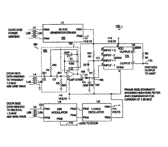
FIG. 13 provides an illustrative schematic diagram of a circuit 148 that
may be implemented on the frame side of the alternate embodiment of the
present invention. Circuit 148 comprises power winding set L5 connected to a
20
KHz generator driver 150. The generator 150 drives the primary coil L5a of the
power winding set L5 in order to provide power from the frame side to the door
side. A more detailed view of the generator is illustrated in Fig. 14.
As shown in FIG. 14, the generator 150 generally comprises a rectifier-
filter 152, a sine wave oscillator 154 and a two stage push-pull driver 156.
The
generator driver 150 is utilized to provide frequencies in the high audible
range or
above, so that a person with a normal hearing range or frequency would not be
disturbed by the sounds emanating from the device. A traditional power supply
source of 120 VAC is applied to a center tapped transformer L7 to provide 24
VAC. The output of the transformer L7 is rectified utilizing diodes D1, D2,
D3, D4
and then filtered by capacitors Cl, C2. The filtered signal powers the dual op
amp sine wave oscillator 154. Sine wave Oscillator 154 comprises dual
operational amplifiers U1, U2.
The sine wave oscillator 154 generates a sine wave by first generating a
square wave, at the required frequency, utilizing amplifier U1 which is
configured
as an astable oscillator with a frequency that is determined by R1 and C3.
Amplifier U2 provides a low pass filter that filters the square wave output
from
Ul. The filter U2 is configured to have a cut off frequency equal to the
square
wave frequency from U1 and thus provides a sine wave at a frequency
determined by the associated circuit component resistors and capacitors.
In this embodiment, the desired frequency of 20,000 Hz is attained by
providing a
capacitor C3 having a value of 0.0047 pfd and based on these values, the
(1551811: )
17
CA 02792041 2012-10-11
values of components R1, C9,C10 and R12 are then calculated. The relevant
equations for the component selection may be described as follows:
C9 = C3
C1 0=2C1
R1 = 1/2 F /(.693 * C1)
R12 = 1/ (8.8856*F*C1)
R13 = R12
Accordingly, the following exemplary values which are also shown in the
circuit 148 are determined to be as follows:
09 = C3 = 0.0047 pfds
C10 = 2C1 = 0.01 pfds
R1 = 1/2 F 4.693 * C1) = 7.5 KOhms
R12 = 1/ (8.8856*F*C1) = 1200 Ohms
R13 = R12 = 1200 Ohms
Resistors R3 and R6 are selected to be 1K Ohms each and are matched
in value to help minimize errors in the actual frequency of operation. The
frequency F is the required sine wave frequency - 20,000 Hz. The value for Cl
is
selected arbitrarily, with a value of 0.0047 pfd being a good initial value
for 20
KHz.
The output of the sine wave generator 154 is connected to the two-stage
push-pull driver 156 in a dual rail through capacitors C5, 08. The output 158
of
the two stage push-pull driver is connected to the primary winding L5a and
capacitor 04 in parallel to cause resonance at 20 KHz. This provides power
from
the frame side to the door side. The generator 150 is essentially a dual rail
system that is capable of providing approximately 28 volt peak to peak signal
to
the primary winding L5a of the power link split core transformer 20.
Returning to the schematic diagram of FIG. 13, that is, the frame side
circuit, a coil winding set L4 enables communication to be received on the
frame
side from the door side. As illustrated, the door side would provide a 1.3 Mhz
1551S11;
18
CA 02792041 2012-10-11
carrier modulated by an Amplitude Shift Keying (ASK) signal to coil L4b. The
induced modulated signal is picked up by coil L4a and passed through a third
order high pass filter 160. The third order filter 160 removes the 20 KHz
power
signal which may be several times stronger than the modulated carrier.
Third order high pass filter 160, comprises an inverting first order filter
162
coupled with a non-inverting second order filter 164. The first order filter
162 is
comprised of resistor R1 and capacitor Cl. The second order filter 164
comprises capacitors C2, C3 and resistors R4, R5. The output 166 of the high
pass filter 160 is applied to a rectifier diode D1 and filter capacitor C4 to
convert
a group of positive going half cycles to a single positive pulse. In
operation, each
positive pulse from the rectifier is an accumulation of approximately twelve
half
cycles of the carrier signal of 1.3Mhz. In effect, this yields a maximum data
rate
on the order of approximately 100 KB, which is determined as follows:
1300000 / 12 = 108333.333 bps
The rectified and filtered signal 168 is then applied to the negative input of
a
comparator 170. A sliding threshold signal 171 is applied to the positive
input of
the comparator 170. Comparator 170 may be a device such as an LM393 made
by National Semiconductor of Santa Clara, California. The output 172 of the
comparator 170 may then be supplied directly to a serial input data conversion
device such as a Universal Asynchronous Receiver Transmitter (UART). The
UART provides conversion of the serial stream to a parallel data stream for
use
by other devices.
The transmission of data from the frame side to the door side is
accomplished by utilizing a carrier frequency which is provided by the
oscillator
U5. Oscillator U5 provides a 1.3 Mhz carrier signal that is connected to ASK
modulator U4. Data 175 that is to be transmitted is then applied to the
modulator
U4 to provide an output signal 173. Output signal 173 is applied across coil
L6a
to induce a current in coil L6b on the door side where the data 175 may the
parsed and utilized.
Turning next to the door side of the second embodiment of the present
invention, FIG. 15 provides an illustrative schematic diagram of a circuit 174
as
( 1551811 : )
19
CA 02792041 2012-10-11
implemented on the door side of this alternate embodiment. Similar to the
frame
side, circuit 174 comprises power winding set L5 and data windings L4, L6.
Power from the frame side is provided through primary winding L5a and
induces a current in secondary winding L5b. Capacitor C6 is in parallel with
secondary winding 5b to cause resonance. The secondary winding L5b is in
electrical connection with bridge rectifier D3. Bridge rectifier D3 converts
the
received sine wave to a full wave rectified signal 176. A filter capacitor C5
is
located in parallel across the output terminals of the rectifier Dl. The full
wave
rectified and filtered signal 176 is applied to a voltage regulator U1.
The regulator U1 provides the necessary voltage V.ut to charge a built-in
battery BAT1 and provide power to the door side circuit 174. A voltage
regulator
such as LM 317, available from National Semiconductor Corp., Santa Clara,
California, meets the necessary specifications to support the configuration of
this
embodiment of the present invention.
The power winding set L6 enables communication that originates on the
frame side to be received on the door side. The frame side produces a 1.3 Mhz
ASK sine wave in coil L6a, which in turn induces a current in coil L6b on the
door
side. The induced modulated signal is then passed through a third order high
pass filter 180 (Fig. 15).
Similar to the frame side, the Third order high pass filter 180, comprises
an inverting first order filter 182 coupled with a non-inverting second order
filter
184 to produce a rectified and filtered signal 186. The rectified and filtered
signal 186 is then applied to a rectifier diode D1 and filter capacitor C4,
and then
to the negative input of a comparator 188. Comparator 188 may be a device
such as an LM393 made by National Semiconductor of Santa Clara, California.
The output 190 of the comparator 188 represents digitized data received from
the
frame side.
Winding set L4 as previously described, enables communication to be
received on the frame side from the door side. As illustrated, the door side
would
provide a 1.3 Mhz carrier utilizing the oscillator U5, the output of which is
modulated by an Amplitude Shift Keying (ASK) modulator U4. Modulator U4
( 1551811 : I
receives outgoing data 192. Outgoing data 192 is information that is present
on
the door side for transmission to the frame side. A modulated signal 194
comprising the outgoing data 192 is provided at coil L4b. Through induction,
the
modulated signal 194 is picked up by coil L4a on the frame side where the data
can be extracted as described above relative to the signal that is picked up
by coil
L6b on the door side.
In a further aspect of the present invention, identical carrier frequencies
may be utilized to transmit data in both directions such that both receivers
would
output the same data for transmission in either direction. In an even further
aspect, different frequencies, which are separated by a sufficient amount to
allow
the use of band pass filters for distinguishing between power frequency of
door or
frame transmitters may be utilized. A resulting reduced data rate may occur in
this instance due to bandwidth limitations.
While protruding assembly 12 and receiver assembly 18 have been
described herein as separate assemblies, it is contemplated by this invention
that
the protruding assembly may be made part of and combined with a conventional
door latch bolt assembly and the receiver assembly may be made part of and
combined with a conventional strike assembly.
Referring to FIG. 16 through 18, an alternative embodiment of an
inductively coupled power transfer entry device system is generally indicated
by
reference numeral 800. In a preferred embodiment, entry device system 800 is
substantially a mortise lock set having a door unit 801 and a frame unit 802.
Door
unit 801 comprises a lock body 820 that is inserted within a mortise 821 cut
into
the edge 823 of a door proportioned so as to create a snug fit between the
body
and door. Face plate 824 covers any gaps between the body and the face of the
door and also protects the internal mechanisms housed with the body. Face
plate
824 is generally adapted to fit flush with the edge surface of the door when
secured. Lock body 820 is equipped with a door latch 822, a dead latch 825,
and
a deadbolt slide (now shown). Door latch 822 passes through latch aperture 864
on strike plate 863 and engages within a recess in the door frame so as to
secure
the door in a closed position. Generally, a handle (not shown) is used to
operate
a latch mechanism which allows latch 822 to be
21
CA 2792041 2017-10-11
CA 02792041 2012-10-11
selectively withdrawn into the lock body and out of the recess, thereby
allowing
the door to swing open from the door frame. While lock body 820 is further
typically equipped with a deadbolt and associated mechanism to provide a
further structural locking means, the embodiment shown in FIG. 16 replaces the
typical deadbolt slide with an inductively coupled power transfer receiver
unit
(second transformer core portion) 830. Similarly, strike plate 863 of frame
unit
802 is equipped with a corresponding inductively coupled power transfer
transmitter unit (first transformer core portion) 818 situated proximate the
opening typically reserved within the dust box for passage of the deadbolt
slide
when the deadbolt is engaged. Thus, it is envisioned that mortise locks
currently
mounted within homes and businesses can be retrofitted with the present
embodiment without requiring additional cutting of the door, frame or
hardware.
Referring now to FIG. 17, frame unit 802 is generally comprised of a strike
plate 863 having apertures 864 and 866. Aperture 864 is sized to accept
insertion of a latch 822 (see FIGS. 16 and 18) when strike plate 863 is
properly
positioned and secured on a frame. In a typical mortise lock set, aperture 866
is
sized and positioned so as to accept passage of a deadbolt slide. However, in
the presently envisioned embodiment, aperture 866 is equipped with transformer
core portion 818 having a front cover (not shown), preferably slightly
recessed,
and a back cover 850. Positioned between the covers of the transformer core
portion is a transformer core half, such as for example pot core half 852,
having
sides 853 and a central open cylindrical post 851, defining opening 855. Width
W1 of core half 852 is sized to fit within opening 866. Coils 854 are wrapped
around bobbin 856, with the wound bobbin placed around central post 851 and
proportioned to rest within sides 853 of the core half. An electrical current
is
applied to coils 854 by conventional wiring (not shown) to generate a magnetic
field. The core half focuses the strength of the magnetic field while sides
853
provide shielding to reduce electromagnetic interference. When the charged
transformer core portion is brought into close proximity to a corresponding
uncharged transformer core portion, the magnetic field generated by the
charged
transformer core portion induces a current within the uncharged transformer
core
1551811: }
22
CA 02792041 2012-10-11
portion. This induced current can then be directed to charge a battery or
supply
power to selected electronic components, e.g. an electronic key pad.
Importantly, the covers and bobbin are fabricated from non-ferromagnetic
materials so as to not attenuate the magnetic fields generated by the coil and
core.
FIG. 18 provides an exploded view of second transformer core portion 830
used in conjunction with the mortise lock set. Transformer core portion 830 is
comprised of a transformer core half, such as for example pot core half 841
having sides 842 and a central cylindrical post 843 defining opening 845.
Width
W2 of core half 841 is sized to fit within the opening in the lock body
typically
occupied by a dead bolt slide. Coils 833 are wrapped around bobbin 835, with
the wound bobbin positioned so as to be around post 843 and within sides 842.
When the door is closed within the frame, coils 833 are induced by the
external
magnetic field generated by transmitter coils 854 to generate an electric
current.
The core half focuses the strength of the magnetic field, thereby producing
higher
current. The induced current can then be used to recharge a battery, power a
remote keypad or enable any other feature requiring electrical power. Core
half
841, with associated bobbin and coils, is housed between push plate 838 and
cover 840. Importantly, bobbin 835 and cover 840 cannot be constructed of
ferromagnetic material as this would interfere with the desired reception of
the
external magnetic field, thereby interfering with electrical current
generation.
Spring 846 is mounted to the back face of push plate 838 and biases
transformer
core portion 830 towards the corresponding transformer core portion 818 within
frame unit 802 such that cover 850 of the transformer core portion 830
contacts
the aperture cover of the transformer core portion 818 when the door is in the
closed position. Ramp taper 844 on cover 840 serves to allow cover 840 to
ramp.
into alignment with the slightly recessed cover of transformer core portion
818
when the door is moved to a closed position. Thus, the distance between the
two core halves (841 and 852) is always maintained at a controlled, fixed
distance when the door is closed. By maintaining a fixed gap, resonance
( 1551611 I
23
CA 02792041 2012-10-11
between the transmitter and receiver is optimized thereby allowing for
transmission of the maximum amount of energy between the pot cores.
Core halves 852 and 841 as shown and described with reference to FIGS.
16-18 may be of any suitable size and dimension. However, it is envisioned in
systems which retrofit or are to be configured to be housed within traditional
mortise lock sets, the cores of the core halves are generally configured to
have
only partial side walls 853 and 842, respectively, so as to fit and freely
move
within the existing cutouts for the deadbolt slide. The deadbolt cutout is
generally
about three quarters of one inch (3/4") wide and about one and one half inches
(1
1/2") high. Ideally, the core halves and coils are of the largest size
permissible as
the larger the size core and coil, the stronger the produced magnetic field at
the
transmitter and the stronger the current induced at the receiver.
It is understood that various configurations of cores may be used such as
for examples, U-shaped core halves, E-shaped core halves, cylindrical shaped
core halves and pot core halves. In one aspect of the invention where a pot
core
configuration is used, a pot core such as Part # 18-11-11, available from TSC
Ferrite International, Wadsworth, Illinois, meets the necessary specifications
to
support the configuration of this embodiment of the present invention.
A further embodiment of an inductively coupled power transfer entry
device system as shown in FIGS. 16 through 18 includes provision of light
pipes
or fiber optic cables situated within opening 845 of core half 841 of
transformer
core portion 830, and within opening 855 of pot core half 852 of transformer
core
portion 818 so as to provide for data communication between door unit 801 and
frame unit 802. Ideally, the fiber optic cable within core half 841 is a
bundle of
individually clad fibers arranged in coaxial orientation to form a single
cable such
that receiving fibers 831 are centrally located within the cable's core, with
emitting fibers 832 arranged circumferentially around the core to create a
general
bull's eye pattern of optic fibers. Conversely, the fiber optic cable within
core half
852 may be arranged as a coaxial bundle of individually clad fibers with the
emitting fibers 862 situated at the cable's core and the receiving fibers 861
arranged circumferentially around the emitting fibers. (See FIG. 19 and
relevant
(1551811: )
24
CA 02792041 2012-10-11
discussion thereof, below). Cover 840 of transformer core portion 830 and the
front cover of transformer core portion 818 are transparent so as not to
impede
transmission of light signals from emitting fibers 832 and 862. As shown in
FIG.
20, light signals 895 are transmitted from one unit and received by the second
unit. While shown as one-way communication, it is to be understood that each
core half can transmit and receive light signals from the opposing core half.
Note
that, in one aspect of the invention, the particular core and cladding
materials of
the fibers may be selected to provide a particular Numerical Aperture (NA) of
approximately 0.6. An NA of approximately 0.6 will provide light rays that may
be
accepted from light sources and light rays transmitted by the fiber in a cone
having an included angle of approximately 600 about the axis of the fiber.
This
permits the ends of the mating fibers to be misaligned somewhat and still
capture
the emitted light.
Communication between door unit 801 and frame unit 802 may be for the
purpose of exchanging information regarding such things as lock status or the
keyed or inputted entry data provided at the lock, or to enable the
reconfiguration
of an electric lock with a new combination. In one example, an infrequently
used
character may be periodically transmitted from the door to the frame to
indicate
that the door is closed. If the character fails to arrive at the frame within
a
specified period of time, an alarm is sent to a host or system administrator
advising an insecure status. The fiber optic cables provide the ability to
transmit
data at a rate of up to 100 K Baud between the frame and the door.
In FIG. 19, a further embodiment of an inductively coupled power transfer
entry device system is indicated generally by reference numeral 899. Entry
device system 899 is generally comprised of a first transformer core portion
870
to be housed within a door and a corresponding second transformer core portion
880 to be housed within a frame. Each of transformer core portions 870 and 880
are fixedly mounted to its respective door or door frame, with the gap between
the units defined by the gap between the door and the frame. Thus, while the
individual gap is fixed and defined between a particular door and its
particular
frame, the gap distance may vary for one door/frame unit to the next. As the
gap
(1551811:
CA 02792041 2012-10-11
between the door and frame (and the associated core portions housed in each)
is
considerably greater than when using a spring-based system which biases one
transformer core portion into near contact with its corresponding counterpart,
the
paired resonating circuits of the fixed transformer core portions are off-
tuned so
as to yield a more constant output level over the wider gap space. This off-
tuning
of the resonant circuitry is discussed in more detail below, with reference to
FIGS. 24 and 25.
Similarly to the modified transformer core portions described above with
reference to FIGS. 16-18, each of transformer core portions 870 and 880 is
comprised of a core half, such as for example pot core halves 873 and 883,
respectively, having a side wall and an internally open cylindrical post 875.
Housed between the side wall and post is a bobbin (874 and 884, respectively)
wound with coils. Electrical current is supplied to the set of coils wrapped
around
bobbin 884 by the circuit including electrical connection 889. The supplied
current generates a magnetic field emanating from the coils on bobbin 884. If,
and when, transformer core portion 870 is sufficiently within the magnetic
field
generated by transformer core portion 880, an induced electrical current is
generated by the coils wound around bobbin 874. This induced electrical
current
is then transferred to any desired electrical device by electrical connection
879.
Examples of a desired electrical device include, but are not limited to, an
electric
lock or electric key pad.
Ideally, each transformer core portion 870 and 880 will have an external
width less than one inch (1") as current fire codes for fire door applications
restrict bore hole sizes to one inch or less. A pot core such as Part #22-13-
00,
available from TSC Ferrite International, Wadsworth, Illinois, meets the
necessary specifications to support the configuration of this embodiment of
the
present invention.
Similarly as described above with reference to the transformer core
portions in FIGS. 16-18, the transformer core portions of the embodiment shown
in FIG. 19 may each further incorporate a fiber optic cable, e.g. reference
numeral 876 within the core's open internal cylinder. The fiber optic cable
within
( 1551811 : )
26
CA 02792041 2012-10-11
core 873 of first transformer core portion 870 is comprised of a bundle of
individually clad fibers arranged in coaxial orientation to form a single
cable such
that receiving fibers 871 are centrally located within the cable's inner core
877,
with emitting fibers 872 arranged circumferentially around the core to create
a
general bull's eye pattern of optic fibers with the receiving fibers located
at core
877 and the emitting fibers forming a circular region 878 thereabout.
Conversely,
second transformer core portion 880 is equipped with a fiber optic cable
within its
respective core 883 comprising emitting fibers 882 and receiving fibers 881.
Complementary to the arrangement of fibers in transformer core portion 870,
the
emitting fibers of transformer core portion 880 are individually clad fibers
situated
at the cable's core while the receiving fibers are individually clad fibers
arranged
circumferentially around the emitting fibers in a coaxial orientation. With
this
arrangement, two-way communication between the frame and door is conducted
as light signals are transmitted from one transformer core portion and
received
by the other transformer core portion. Communication between first transformer
core portion 870 and second transformer core portion 880 may be for the
purpose of exchanging information regarding such things as lock status or the
keyed or inputted entry data provided at the lock, or to enable the
reconfiguration
of an electric lock with a new combination. The fiber optic cables provide the
ability to transmit data at a rate of up to 100 K Baud between the frame and
the
door.
As exemplified by the schematic of FIG. 20, light signal 895 is being
emitted by the fiber optic cable within second transformer core portion 880.
The
fiber optic cable is selected to have an NA of 0.60, and the included angle of
the
emitted light cone of light shown is approximately 60 . As can be seen in FIG.
20, even permitting some degree of axial misalignment between the mating fiber
optic cables (shown by the double headed arrow), receiving fiber optic cable
871
remains within the splayed pattern of the emitted light.
In another aspect of the present invention with reference to the
embodiments depicted in FIGS. 16-20, circuits are introduced into the door and
frame side to maximize the power transfer and bi-directional data transfer
across
(1551811: )
27
CA 02792041 2012-10-11
the gap that exists between the transmitting and receiving cores of the
present
invention.
Referring now to FIGS. 21 through 24, the present invention further
comprises circuitry of components that are utilized to provide the necessary
signaling between door unit 830, 870 and frame unit 818, 880. Some of the
circuitry is located on or within the door and some on or within the frame.
When the door is in the closed position within the frame power transfer
transmitter unit 818 is adapted and aligned to receive the protruding ramp 844
in
a fit and manner as to align the opposing pot core transformers and to
minimize
air gap therebetween. This closed door configuration of the transformers
enables the transfer of power and data between the door unit 830, 870 and
frame
unit 818, 880 when power is applied to the frame side by utilizing circuits
that are
present in door in cooperation with a frame portion circuit.
FIG. 21 is a schematic diagram of an exemplary simulation circuit for
implementing the power and data transmission features of the present
invention.
Specifically, circuit 1002 is representative of the door circuitry and circuit
1004 is
representative of the frame circuitry. The various components of simulation
circuits 1002, 1004 provide recharging of batteries, by power transfer, and
importantly provide resonance between the transmitter and receiver to enhance
the amount of energy that is transferred between the two. Door circuit 1002
comprises a resonating capacitor 1006, a direct current (DC) load 1008, and
secondary coil 1010. The resistance of the wires and other circuit components
is
represented by wire resistance 1012. Similarly, simulation frame circuit 1004
comprises a resonating capacitor 1014, primary coil 1016, a DC voltage source
1018 and wires/component resistance 1020.
In an embodiment of the present invention, wherein there is a variable gap
between the door unit 870 and frame unit 880 (FIGS. 19-20) having a range of
between approximately 0.04 to 0.375 inches, the resonant circuits 1002, 1004
are off-tuned to thereby yield a more constant output level across the gap, It
should be noted that this embodiment of the invention provides power
transmission for charging system batteries along with data transmission
between
( 1551811 : 1
28
CA 02792041 2012-10-11
the door and frame across the gap. Frequency tuning of the circuits 1002, 1004
is accomplished by altering the capacitance of each of the respective
resonating
capacitors 1006, 1014.
Turning next to Figure 22, details for an exemplary embodiment of a frame
side transmission circuit 1020 is shown. The circuit 1020 comprises among
other components a power circuit 1022, a timing oscillator U7, a bridge driver
U8,
and a coil L8 to convert a 24 volt DC input into a flux signal operating at
approximately 100+ KHz.
The power circuit 1022 comprises a power input block P1, a poly fuse Fl
a bridge rectifier D12, a transient voltage suppressor R13, a voltage
regulator U6
and a decoupling capacitor C11. As shown, DC power IN+ and IN- at
approximately 24 Volts is applied to power block P1 and thus to the frame
circuit
1020. The poly fuse Fl is connected in series with the input DC power to
provide
protection to the upstream power source powering frame circuit 1020. Also
providing circuit protection is the suppressor R13. The rectifier D12 is
connected to the fuse Fl and ensures that the correct polarity is supplied to
the
balance of the electronics / circuitry regardless of the polarity of the input
voltage
that is applied. A voltage VIN at approximately 24 Volts can then be obtained
across the bridge rectifier D12. Voltage VIN is applied to the voltage
regulator U6
to convert the 24 volts DC to 5 volts DC (VCC) for use by other circuit
components U7 and U8. Output voltage VCC is provided across decoupling
capacitor C11 to accommodate any variations in current draw from the balance
of the frame circuit 1020.
In an embodiment of the present invention, timing oscillator component U7
is an RC timer oscillator having connected thereto voltage VCC to power the
component U7, receives trigger signals across resistor R14 and capacitor C12,
and provides the required timing utilizing a capacitor C13 and a resistor R15.
The output pulse width is controlled by the values and combination of the
external resistor R15 and capacitor C13. In the preferred embodiment
illustrated
herein, the time triggered signal outputs is a 5 volt square wave signal. The
square wave signal is in turn provided to the bridge driver U8.
( 1551811 : )
29
CA 02792041 2012-10-11
Driver U8 is an "H Bridge driver", which provides a 24 volt square wave
output that is simultaneously available in both phases, to drive the primary
winding L8 of the Inductive Coupled Power Transfer (ICPT) unit through a
resonant capacitor C14.
Figure 23 illustrates an exemplary implementation of a receiving door
circuit 1024 for the door side of the present invention. In operation, the
circuit
1024 receives signals from a secondary coil P2 of the ICPT, rectifies and
filters
the signal to provide 12/24 volts DC output, for providing power on the door
side.
The secondary coil P2 is center tapped thereby allowing the full winding to be
used for 24 volt output while half of the winding will yield a 12 volt output.
Resonant capacitors C17 and C18 are connected to the coil P2 to provide
resonant coupling between the primary P1 and secondary P2 windings. A
connector block P3 is provided to enable jumpers to be placed so as to provide
ground at either the anode of zener diodes D10 or D11. The diodes D10, Dll
regulate the 12/24 volt output (Vout)of circuit 1024 that is provided at block
P4.
A capacitor C19 is provided to filter the high frequency ripple on the output
voltage Vout.
As previously stated, an aspect of the present invention is optimizing the
resonance between the transmitter and receiver in order to maximize the amount
of energy transferred therebetween. This aspect is further illustrated in the
graphical representations of Figures 24 and 25 which are described below.
Figure 24 illustrates the results from tuning the resonant circuits of each
pot core transformer to the same frequency. A first graph 1026 depicts Vout of
the door side circuit 1002 over a range of gap sizes. A second graph 1028
depicts the input current (lin) to the frame side circuit 1004 over a range of
the
gap sizes. As illustrated, it takes more current lin as the cores move farther
apart
i.e. gap increases.
Figure 25 illustrates the results from off tuning the resonant circuits of
opposing pot core transformers i.e. utilizing different frequencies, meaning
utilizing different values for resonating capacitors 1006, 1014. A first graph
1032
depicts Vout of the door side circuit 1002 over a range of gap sizes. A second
(1551811: I
CA 02792041 2012-10-11
graph 1034 depicts the input current (lin) to the frame side circuit 1004 over
a
range of the gap sizes. While the output voltage Vout is more consistent over
the
full gap range, a small price in efficiency is paid. It should be observed
that the
input current that is required over the same gap range of the matched
resonance
arrangement is comparatively higher.
As used herein efficiency is defined as :
((Vout)2) /( RLOAD / (Vin * lin))
While the invention has been described with reference to preferred
embodiments, it will be understood by those skilled in the art that various
changes may be made and equivalents may be substituted for elements or
components thereof to adapt to particular situations without departing from
the
scope of the invention. Therefore, it is intended that the invention not be
limited
to the particular embodiments disclosed as the best mode contemplated for
carrying out this invention, but that the invention will include all
embodiments
falling within the scope and spirit of the following claims.
( 1551811:
31