Note: Descriptions are shown in the official language in which they were submitted.
CA 2,835,035
Blakes Ref: 77505/00009
1 SYSTEM AND METHOD FOR DECODING A RADIO SIGNAL
2
3
4 [0001] [INTENTIONALLY DELETED]
6
7
8 TECHNICAL FIELD
9 100021 The present invention relates to radio communication
systems, and in particular to
software defined radio systems.
11
12 BACKGROUND OF INVENTION
13 100031 Traditionally, development of radio communication products
involves significant
14 hardware development effort. Software defined radio (SDR) is a
technology that implements
.. physical layer wireless communication technologies in software, turning
many radio-related
16 hardware development problems into software issues. This can shorten the
product
17 .. development cycle, reduce costs, and make product distribution much
easier. Moreover, SDR
18 provides increased flexibility and programmability, which can speed up
innovation in
19 wireless communications.
[0004] SDR platforms have been developed using a personal computer's
central
21 .. processing unit (CPU), working in connection with a field programmable
gate array (FPGA),
22 with some radio frequency (RF) front end hardware to receive and
transmit radio waveforms.
23 Some SDR applications require complex modulation or computationally
intensive algorithms
24 that may include Fast Fourier Transforms (FFTs), cross-correlation, or
the calculation of
mutual information metrics. These operations can be costly in terms of
processing power. A
26 CPU working in connection with an FPGA may lack the computing
architecture to support
27 these applications. More recently, SDR platforms have been developed
using a CPU working
28 in connection with a graphics processing unit (GPU). However, a GPU
working in
- 1 -
23286761.1
CA 2835035 2018-01-08
CA 02835035 2013-11-04
WO 2012/151662
PCT/CA2012/000314
1 connection with a CPU may lack the streaming or serial processing
capabilities to fulfill the
2 real-time requirements of digital communication algorithms that perform
serial processing.
3 [0005] It is an object of the present invention to obviate or
mitigate at least one of the
4 above disadvantages.
6 SUMMARY OF THE INVENTION
7 [0006] In one aspect, a method of decoding a radio signal by an
electronic device is
8 provided. The method includes receiving the radio signal, digitizing the
radio signal, auto-
9 correlating the radio signal to generate a first signal and determining
periodic information of
the radio signal using the first signal.
11 [0007] In another aspect, an electronic device, such as an SDR
device, is provided. The
12 electronic device includes a RF front end, a processing unit and memory,
the memory storing
13 computer executable instructions that when executed by the processing
unit, causes the
14 electronic device to receive the radio signal, digitize the radio
signal, auto-correlate the radio
signal to generate a first signal and determine periodic information of the
radio signal using
16 the first signal.
17 [0008] The processing unit may include an FPGA in communication
with the RF front
18 end. The FPGA can perform serial processing on the digitized radio
signal provided by the
19 RF front end. The processing unit may also include a GPU in
communication with the FPGA
for performing parallel processing on the digitized radio signal provided by
the FPGA.
21 [0009] In another aspect, a computer readable storage medium for
decoding a radio signal
22 by an electronic device is provided. The computer readable storage
medium includes
23 computer executable instructions that when executed by a processing
unit, causes the
24 electronic device to receive the radio signal, digitize the radio
signal, auto-correlate the radio
signal to generate a first signal and determine periodic information of the
radio signal using
26 the first signal.
27 [0010] In another aspect, an electronic device is provided. The
electronic device includes
28 a radio frequency front end for receiving electromagnetic radiation and
digitizing the
29 electromagnetic radiation to generate a digital signal. The electronic
device also includes a
field programmable gate array in communication with the radio frequency front
end. The
- 2 -
CA 2.835,035
Blakes Ref: 77505/00009
1 field programmable gate array is optimized for performing serial
processing. The electronic
2 device also includes a graphics processing unit in communication with the
field
3 programmable gate array optimized for performing parallel processing.
4
BRIEF DESCRIPTION OF THE DRAWINGS
6 [0011] Embodiments of the invention will be described by way of
example only with
7 reference to the accompanying drawings in which:
8 [0012] FIG. 1 is a block diagram of an example SDR device;
9 [0013] FIG. 2 is a block diagram of a target monitor receiving an
input signal and
producing an emanation signal that is intercepted by an example SDR device;
11 [0014] FIG. 3 is a block diagram of an example configuration of the
SDR device for the
12 specific application of decoding an emanation signal;
13 [0015] FIG. 4 is a schematic diagram of an example radio frequency
front end;
14 [0016] FIG. 5 is a flow chart of an example process for decoding
the input signal of a
target monitor from its electromagnetic radiation using an example SDR device;
16 [0017] FIG. 6(a) is a front view of a target monitor displaying an
example 2 by 2 pixel
17 image and FIGS. 6(b) and (c) are corresponding input and emanation
signals thereof,
18 respectively;
19 [0018] FIG. 7 is a flow chart of an example initialization process
for an example SDR
device;
21 [0019] FIGS. 8(a) to (e) are example waveforms of an auto-
correlated signal and the
22 Fourier Transform thereof;
23 [0020] FIGS. 9(a) and (b) are waveforms corresponding to an example
demodulated
24 signal; and
[0021] FIG. 10 is a block diagram of an example application layer of the
SDR device.
26
27 DETAILED DESCRIPTION OF THE INVENTION
28 [0022] It will be appreciated that for simplicity and clarity of
illustration, where
29 considered appropriate, reference numerals may be repeated among the
figures to indicate
-3-
23286761.1
CA 2835035 2018-01-08
CA 02835035 2013-11-04
WO 2012/151662
PCT/CA2012/000314
1 corresponding or analogous elements. In addition, numerous specific
details are set forth in
2 order to provide a thorough understanding of the example embodiments
described herein.
3 However, it will be understood by those of ordinary skill in the art that
the example
4 embodiments described herein may be practised without these specific
details.
[0023] In other instances, well-known methods, procedures and components
have not
6 been described in detail so as not to obscure the example embodiments
described herein.
7 Also, the description is not to be considered as limiting the scope of
the example
8 embodiments described herein.
9 [0024] Turning to FIG. 1, a schematic diagram of an example SDR
device 10 is provided.
In this example, the SDR device 10 includes a RF front end 12 having an
antenna 28 for
11 receiving and converting electromagnetic radiation into a digital
signal, a field programmable
12 gate array (FPGA) 14 for performing high speed serial processing and a
graphics processing
13 unit (GPU) 16 for performing parallel processing. The SDR device 10 may
also include a
14 general purpose computer processing unit (CPU) 18 for performing general
computations
including providing the user interface and programming the FPGA 14 and GPU 16.
The
16 FPGA 14, GPU 16 and CPU 18 can each have its own memory 15, 17 and 19,
respectively
17 and/or can access a separate memory component 13 of the device 10. It is
understood that the
18 FPGA 14 can include any suitable programmable logic device and GPU 16
includes general
19 purpose computing on graphics processing unit ((GP)GPU).
[0025] In the example of FIG. 1, the RF front end 12 is connected to the
FPGA 14 and is
21 operable to communicate with the FPGA 14 by a plurality of digital
signals. The FPGA 14,
22 GPU 16 and CPU 18 are connected to one another by a high speed bus 21,
such as a
23 Peripheral Component Interconnect Express (PCIe) bus, for example.
24 [0026] The SDR device 10 enables rapid serial and parallel
computation of signal
processing data. For example, the SDR device 10 can divide signal processing
algorithms
26 into block and streaming processes and implement the block and stream
processes to
27 optimize processing efficiency. Stream processing may segment the input
signal into a
28 plurality of discrete segments or "chunks" based, in part, on the
current state of the input
29 signal passing through it, while block processing may comprise fixed,
invariant, processing
on each chunk.
- 4 -
CA 02835035 2013-11-04
WO 2012/151662
PCT/CA2012/000314
1 [0027] In one example SDR device 10, the FPGA 14 is optimized to
provide a serial
2 processing environment to perform stream processing faster than the GPU
16. The GPU 16
3 is optimized to provide a parallel processing environment to parallelize
block processes faster
4 than the FPGA 14. The GPU 16, thus effectively implements parallelizable
calculations and
algorithms, including, for example, weak signal reconstruction, auto-
correlation, FFTs,
6 mutual information metrics, as well as concurrent processing of arbitrary
algorithms or
7 calculations on single or multiple data streams.
8 [0028] The programmability of the FPGA 14 and the GPU 16 also
provides flexibility,
9 such that the SDR device 10 may be capable of running arbitrary wireless
protocols. For
example, FPGA 14 and GPU 16 can be reprogrammed by CPU 18 during operation to
handle
11 changes in the communication protocol of the input signal. Once
programmed, the SDR
12 device 10 can autonomously store and send data without requiring
additional configuration or
13 intervention.
14 [0029] The SDR device 10 can also be configured to concurrently
monitor spectral and
network resources and adjust transmission and receiving parameters
accordingly.
16 Furthermore, the SDR device 10 can manage its own resources (e.g.. FPGA
14 and GPU 16)
17 such that tasks are efficiently allocated to the appropriate component
based on the type of
18 computation and resource usage.
19 [0030] In an example application of the SDR device 10, it is
operable to identify and
intercept electromagnetic radiation emanating from an electronic device and to
decode the
21 electromagnetic radiation. For example, computer monitors, keyboards,
cellular phones,
22 pagers and RFID readers and tags can emit various forms of
electromagnetic radiation such
23 as radio waves when in operation. The electromagnetic radiation of an
electronic device may
24 be related to the input signal processed by that device. When
electromagnetic radiation is
emitted from an electronic device in the form of radio waves, the SDR device
10 is operable
26 to intercept these radio waves a distance away from the electronic
device, including through
27 physical barriers such as walls and doors.
28 [0031] In the example of a computer monitor, the SDR device 10 can
receive and decode
29 electromagnetic emanations of the computer monitor, which are related to
its input signal, to
determine the image displayed on the computer monitor. By decoding the
emanation signal,
31 the SDR device 10 can surreptitiously reproduce, or enable reproduction
of the images
- 5 -
CA 02835035 2013-11-04
WO 2012/151662
PCT/CA2012/000314
1 displayed on the computer monitor remotely, without the knowledge of the
computer monitor
2 or its user.
3 100321 Turning to FIG. 2, a block diagram of a target monitor 20
receiving an input
4 signal 24, for example from the target monitor's video interface cable 26
(such as DVI, VGA
or HDMI, for example), is provided. Based on the input signal 24, the target
monitor 20
6 displays an image which also causes the target monitor 20 to produce an
emanation signal 22,
7 in the form of electromagnetic radiation, and specifically radio waves.
The emanation signal
8 22 can be received or intercepted by an antenna 28 of the SDR device 10.
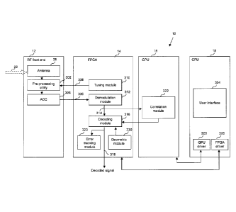
9 100331 Turning to FIG 3, a block diagram of an example
configuration of the SDR device
10 for the specific application of decoding an emanation signal 22 is
provided. The SDR
11 device 10 has an RF front end 12 which includes an antenna 28 to receive
an emanation
12 signal 22, a pre-processing utility 302 to process the emanation signal
22 for digitization, and
13 an analog to digital converter (ADC) 304 to convert the received
emanation signal 22 into a
14 digital signal 306. A tuning module 310 of the FPGA 14 may provide a
tuning frequency 308
to the pre-processing utility 302 to tune the pre-processing utility 302 to a
particular
16 frequency corresponding to the emanation signal 22. The digital signal
306 produced by the
17 ADC 304 is sent to the FPGA 14.
18 [0034] Turning to FIG. 4, a more detailed schematic diagram of an
example RF front end
19 12 is provided. The RF front end pre-processes the emanation signal 22
by amplification and
down-conversion prior to digitization. The RF front end includes an antenna 28
to intercept
21 the emanation signal 22 and may include pre-processing components such
as a low noise
22 amplifier (LNA) 402 to amplify weak signals, a high pass filter (HPF)
404 to filter and pass
23 high frequencies and attenuate low frequencies, an amplifier (e.g. gain
block 406 and/or
24 variable gain amplifier 408), a variable attenuator 410 to vary the
signal gain, a down-
converter 412 to down-convert the signal to baseband, an analog to digital
converter (ADC)
26 304, and a driver 416 and anti-aliasing filter 418 to improve the
quality of the ADC
27 conversion.
28 [0035] In the example of FIG. 4, the RF front end 12 has two modes
of operation, A and
29 B, selectable by a switch 420. Each mode of operation performs a series
of operations on the
emanation signal 22 before digitization by the ADC 304. In FIG. 4, the first
mode of
31 operation A is selected. The emanation signal 22 intercepted by the
antenna 28 is amplified
- 6 -
CA 02835035 2013-11-04
WO 2012/151662
PCT/CA2012/000314
1 by the LNA 402 and filtered using the HPF 404. The gain of the analog
signal is then
2 modified using gain block 406 and variable attenuator 410. The resulting
signal is then
3 down-converted by mixing in a signal generated by the local oscillator
422 using mixer 412
4 to produce a baseband signal. The local oscillator 422 is configured to
generate a signal at
the tuning frequency 308 provided by the tuning module 310 of the FPGA 14. The
baseband
6 signal can be phase shifted by phase converter 424, further amplified by
driver 416 and
7 filtered by anti-aliasing filter 418 prior to digitization using the ADC
304. In this example,
8 the resulting digital signal 306 is decomposed into its quadrature-
carrier (IQ) form
9 comprising an in-phase component 306a, and a quadrature component 306b.
The cut off
frequency of the baseband signal can be determined by the anti-aliasing
filters 418 and can be
11 configured based on the application of the SDR device 10.
12 [0036] By modifying the tuning frequency 308, the SDR device 10
can tune into and
13 isolate an individual emanation signal 22 from one or more emanation
signals received by the
14 antenna 28. For example, the SDR device 10 can isolate an emanation
signal 22 from a
particular monitor from a group of monitors in close spatial proximity, as the
emanation
16 signals associated with each monitor will have a different carrier
frequency.
17 [0037] In the second mode of operation B, the analog signal
received by the antenna 28
18 can be amplified by LNA 402 and filtered using HPF 404, as in first mode
of operation A.
19 However, the analog signal can then be amplified using variable gain
amplifier 408 and
directly applied to ADC 304.
21 [0038] It can be appreciated that the RF front end 12 can be any
appropriate receiver
22 capable of digitizing the emanation signal 22 with a sufficient signal-
to-noise ratio to allow
23 for reconstruction of the input signal 24 of the target monitor 20 by
the SDR device 10. For
24 example, RF front end 12 can be a superheterodyne receiver.
[0039] Turning back to FIG. 3, the SDR device 10 in this example also has
an FPGA 14
26 configured to include a tuning module 310 for providing the pre-
processing utility 302 of the
27 RF front end 12 with a tuning frequency 308, a demodulation module 312
for demodulating
28 the digital signal 306 to produce a demodulated signal 314, and a
decoding module 316 for
29 decoding the demodulated signal 314 to produce a decoded signal 318. The
FPGA 14 can
also include an error tracking module 320 to evaluate the error in the decoded
signal 318 and
31 to initiate error correction.
- 7 -
CA 02835035 2013-11-04
WO 2012/151662
PCT/CA2012/000314
1 [0040] It can be appreciated that the FPGA 14 can have one or more
demodulation
2 modules 312 to carry out demodulation of the emanation signal 22, such as
amplitude
3 modulation (AM), frequency modulation (FM) and single-sideband modulation
(SSB). Each
4 demodulation module 312 can also apply demodulation to one or more
different
communication protocols (for example Global System for Mobile Communications
(GSM) or
6 Zigbee). The modulation techniques and communication protocols can be
configured by the
7 user or provided by third parties. Furthermore, a demodulation module 312
can be
8 reprogrammed during operation to implement a different modulation
technique and/or
9 communication protocol. Accordingly, the demodulation module 312 allows
for different
modulation techniques and communication protocols to be chosen and implemented
on the
11 fly while the device remains operational.
12 [0041] It can further be appreciated that the FPGA 14 can route
the digital signal 306 to
13 one or more of its modules, its internal memory, and/or bypass the FPGA
processing
14 altogether, by configuring the programmable switches provided by the
FPGA. For example,
certain data may not require the use of both the FPGA 14 and GPU 16. Certain
16 communications protocols may be defined and processed entirely within
the FPGA 14 and
17 not require the parallel processing environment provided by the GPU 16.
The selection and
18 passage of the signal within the FPGA 14 can be set according to the
desired application
19 using appropriately configured switches.
[0042] The SDR device 10 in the example also has a GPU 16 configured to
include a
21 correlation module 322 for evaluating the similarities in the
demodulated signal 314 relative
22 to a separation of time (i.e. finding repeating patterns in the
demodulated signal 314) and for
23 providing parameters characterizing that similarity to the decoding
module 316 of the FPGA
24 14. For example, the correlation module 322 is operable to perform cross-
correlation and/or
auto-correlation.
26 [0043] Turning to FIG. 5, a flow chart of an example process for
decoding the input
27 signal 24 of a target monitor 20 from its emanation signal 22 using the
SDR device 10 is
28 provided. At block 500, RF front end 12 intercepts an emanation signal
22 using its antenna
29 28. At block 502, the device 10 obtains the carrier frequency fe of the
emanation signal 22
and specific information related to the input signal 24, such as periodic and
geometric
31 information. At block 504, RF front end 12 tunes into the carrier
frequency by pre-
- 8 -
CA 02835035 2013-11-04
WO 2012/151662
PCT/CA2012/000314
1 processing the emanation signal 22 at the carrier frequency fe. At block
506, RF front end 12
2 digitizes the pre-processed emanation signal using its ADC 304 to
generate a digital signal
3 306. At block 508, FPGA 14 demodulates the digital signal 306 using its
demodulation
4 module 312 to generate a demodulated signal 314. At block 512, FPGA 14
decodes the
demodulated signal 314 using specific information related to the input signal
24 to generate a
6 decoded signal 318. The decoded signal 318 contains all the information
of the input signal
7 24 sufficient to generate an image on another monitor corresponding to
the same image of the
8 input signal 24 on the target monitor 20.
9 [0044] FIG. 6(a) provides an example 2 by 2 pixel image of a
theoretical target monitor
20, and FIGS. 6(b) and (c) provide waveforms of the signals corresponding to
the pixel image
11 of FIG. 6(a). For simplification of understanding, the example of FIG.
6(a) considers a target
12 monitor 20 displaying a 2 by 2 pixel image and having a pixel field of
xt by yt. The pixels p0
13 to p3 make up the image, h0 and hl represent horizontal retrace pauses,
and v0 represents a
14 vertical retrace pause. The horizontal retrace pauses hO, hl transmit
synchronization
information to align the segment of the input signal 24 representing a
horizontal line of a
16 frame (i.e. p0 to pl) to the corresponding horizontal line of the target
monitor 20. The
17 vertical retrace pause v0 transmits synchronization information to align
the segment of the
18 input signal 24 representing a frame (i.e. the image of p0 to p3) to
span the entire display of
19 the target monitor 20, starting with p0 at the top left corner, and
ending with p3 at the bottom
right corner of the target monitor 20 (the retrace pauses are not actually
displayed on the
21 target monitor 20). An example input signal 24 corresponding to the
pixel image of FIG. 6(a)
22 is shown in FIG. 6(b). The parameters l/fh and 1/fv represent the time
necessary for the input
23 signal 24 to represent a horizontal line of the image, and the entire
image, respectively. The
24 parameters f and fh are referred to as the vertical refresh rate and
horizontal refresh rate of
the target monitor 20, respectively. FIG. 6(c) provides an example emanation
signal 22
26 corresponding to the input signal 24 of FIG. 6(b). The example emanation
signal 22 of FIG.
27 6(c) is an amplitude modulated signal of the input signal 24 at a
carrier frequency fc. In order
28 to decode the emanation signal 22 by the SDR device 10, the carrier
frequency fe, periodic
29 information of the input signal 24 (e.g. fh or fv) and geometric
information of the pixel field
(e.g. xt and yt) may need to be determined.
- 9 -
CA 02835035 2013-11-04
WO 2012/151662
PCT/CA2012/000314
1 [0045] As noted above, at block 502, the SDR device 10 obtains the
carrier frequency fc
2 of the emanation signal 22 and specific information related to the input
signal 24. In one
3 embodiment, this information is obtained during the example
initialization process of the
4 SDR device 10 shown in FIG. 7. At block 702, RF front end 12 obtains a
tuning frequency
from the tuning module 310 of FPGA 14. At block 704, RF front end 12 pre-
processes the
6 emanation signal 22 at the tuning frequency using the pre-processing
utility 302. At block
7 706, RF front end 12 digitizes the pre-processed emanation signal using
its ADC 304 to
8 generate a digital signal 306 and sends the demodulated signal to the
demodulation module
9 312 of the FPGA.
[0046] At block 708, FPGA 14 demodulates the digital signal 306 using its
demodulation
11 module 312 to generate a demodulated signal 314. The demodulated signal
314 is then sent
12 to the correlation module 322 of GPU 16.
13 [0047] At block 710, GPU 16 obtains periodic information of the
demodulated signal 314
14 using the correlation module 322. In an embodiment, periodic information
of the
demodulated signal 314 can be obtained by cross-correlating the demodulated
signal 314 with
16 itself (i.e. auto-correlation). For example, a demodulated signal x[n]
can be auto-correlated
17 by computing an auto-correlation function 0[j] = x[m + j]x[m] to
generate an auto-
18 correlated signal, where m spans all the samples of x[n] and j
represents the lag between the
19 instances of x[n] being correlated.
[0048] Referring to FIG. 8(a), an example waveform of an auto-correlated
signal is
21 provided. The peaks of the auto-correlated signal may correspond to
periodic information in
22 the demodulated signal 314. The amplitude is greatest at a lag of 0 when
the demodulated
23 signal 314 is correlated with itself. There can also be significant
correlation when the lag is
24 not 0 since nearby frames in the demodulated signal 314 will be very
similar. For example,
the next highest peak not at lag 0, such as at lag B, can identify the
periodicity of the
26 demodulated signal 314 corresponding to 1/f, (i.e. the length of a
frame) since adjacent
27 frames in the demodulated signal 314 will likely be very similar.
Furthermore, there may be
28 additional peaks spaced apart by approximately one frame length since
nearby frames in the
29 demodulated signal 314 will likely also be similar. The auto-correlated
signal may contain
secondary peaks, such as at lag A or C, corresponding to the length of a
horizontal line within
- 10 -
CA 02835035 2013-11-04
WO 2012/151662
PCT/CA2012/000314
1 a frame, since adjacent or nearby horizontal lines may be similar.
Although the lag has been
2 described in the unit of samples in FIG. 8(a), it will be appreciated
that the unit of samples
3 can be converted to time given the sampling frequency of the SDR device
10. The periodic
4 information (e.g. lify, l/fh, G and/or fh ) can be determined from the
auto-correlated signal
and sent to the decoding module 316 of FPGA 14.
6 [0049] In another embodiment, a Fourier Transform, such as the
Fast Fourier Transform
7 or any other suitable implementation, can be applied to the auto-
correlated signal to improve
8 the extraction of timing parameters fy and/or fh. Referring to FIG. 8(b),
the Fourier
9 Transform of the auto-correlated signal of FIG. 8(a) is provided. As the
auto-correlated
signal will have peaks when the lag is an integer multiple of the frame length
(e.g 1/f,), the
11 Fourier Transform will include a primary peak E at frequency e, which
represents the vertical
12 refresh rate fv. The higher order harmonics at peaks F and G occur at
approximately integer
13 multiples of G.
14 [0050]
As mentioned previously, the periodicity of the horizontal lines may be
captured
by secondary peaks in the auto-correlated signal. For example, the horizontal
line periodicity
16 may be reflected in the Fourier Transform at a peak H of much higher
frequency than G and
17 with significant amplitude greater than peaks F and G of the higher
order harmonics of fv.
18 For example, a computer monitor having a vertical refresh rate f, may be
on the order of less
19 than 100Hz whereas the horizontal refresh rate fh is on the order of
kHz. Therefore, the peak
corresponding to fh may be significantly greater in amplitude than the peaks
of the higher
21 order harmonics of G that may be nearby. The periodic information f
and/or fh can be
22 determined from the Fourier Transform of the auto-correlated signal and
sent to the decoding
23 module 316 of FPGA 14. Applying the Fourier Transform can help to
improve the
24 determination of the timing parameters when the demodulated signal 314
has a low signal-to-
noise ratio.
26 [0051]
In another embodiment, a filter can be applied to the auto-correlated signal
prior
27 to applying the Fourier Transform. Windowing or filtering the auto-
correlated signal may
28 improve recovery of specific timing parameters while suppressing noise
sources and spurious
29 peaks. In the example of FIG. 8(c), a low pass filter is applied to the
auto correlated signal to
attenuate the higher order harmonics in the auto-correlated signal. As a
result, higher order
31 harmonics at peaks F and G, along with peak H shown in FIG. 8(b) are
significantly
- 11 -
CA 02835035 2013-11-04
WO 2012/151662
PCT/CA2012/000314
1 attenuated or absent from the Fourier Transform. Therefore, use of a low
pass filter may
2 simplify the determination of timing information by reducing the number
of peaks to
3 differentiate and identify. It can be appreciated that a high pass filter
can be applied instead
4 of a low pass filter to isolate a different peak in the auto-correlated
signal, for example to
identify fh from the Fourier Transform.
6 [0052] As mentioned above, the use of a filter may be used to
isolate one frequency in the
7 auto-correlated signal. If the demodulated signal 314 includes multiple
sources with similar
8 but unique timing parameters, a filter may help isolate one frequency per
source in the auto-
9 correlated signal and thus enable the SDR device 10 to determine when
multiple sources are
present in the demodulated signal 314, as indicated by the number of distinct
peaks in the
11 resulting Fourier Transform waveform. The frequency at each peak can
then be determined
12 and subsequently used as the respective vertical refresh rate f, when
decoding multiple
13 signals that are superimposed in the demodulated signal 314.
14 [0053] In another embodiment, the correlation module 322 can
evaluate an accuracy or
confidence parameter of the periodic information generated. As mentioned
above, the
16 Fourier Transform of the auto-correlated signal in FIG. 8(b) will
include higher order
17 harmonics at frequencies f and g of frequency e. By definition, the
higher order harmonics
18 should occur at integer multiples of e and thus, peaks E, F and G should
be equal distance
19 apart. In one example, the correlation module 322 can compute frequency
e and the
difference between its higher order harmonics (e.g. f-e, g-h). The mean of the
computed
21 values (i.e. e, f-e, and g-h) can be used as f and the confidence
parameter can be computed as
22 the standard deviation of these values.
23 [0054] In another example, a width of the peak from which periodic
information is
24 obtained may be computed and used as a confidence parameter. In the
example of FIG. 8(c),
frequency e' at peak E' represents the vertical refresh rate fv. The width of
the peak E' can be
26 defined as the distance from the centre (i.e. frequency e') to a
frequency in which the
27 amplitude of the signal decays to a specified fraction (e.g. 1/sqrt(2))
of the maximum
28 amplitude of peak E'. If the confidence parameter is below an acceptable
value, correlation
29 may be repeated until the confidence requirement is satisfied.
- 12 -
CA 02835035 2013-11-04
WO 2012/151662
PCT/CA2012/000314
1 [0055] Referring back to FIG. 7, at block 712, the decoding module
316 obtains
2 geometric information from the geometric module 330. In one example, the
geometric
3 module provides a value of xt and yt chosen from a predetermined set of
values. The
4 predetermined set of values may for example be limited to display
resolutions belonging to
computer display standards set by industry organizations such as VESA.
6 [0056] At block 714, the FPGA 14 decodes the demodulated signal
314 using the
7 periodic information and geometric information to generate a decoded
signal. As part of
8 decoding the demodulated signal 314, the SDR device 10 may determine the
location of the
9 start of each frame of xt by yt pixels within the demodulated signal 314
so that the decoded
signal 318 correctly identifies parts of the demodulated signal 314 that
represent image pixels
11 and horizontal and vertical retrace pauses. This alignment enables the
images represented by
12 the decoded signal 318 to be centred on a computer monitor that displays
the decoded signal
13 318.
14 [0057] In an embodiment, the decoding module 316 can cross-
correlate the demodulated
signal 314 against a reference signal with known synchronization information
(i.e. locations
16 of the horizontal and vertical retrace pauses) that represent a similar
image. The cross-
17 correlated signal may provide a strong peak at the relative offset
between the demodulated
18 signal 314 and the reference signal. Compensating for this offset in the
demodulated signal
19 314 enables the synchronization information of the reference signal to
be applied to the
demodulate signal 314. In one example, the reference signal may be agreed upon
by the
21 target monitor 20 and the SDR device 10. In another example, the
reference signal may
22 include a known image likely to be displayed on the target monitor such
as a menu or start
23 button of a popular operating system. It can be appreciated that
multiple reference signals,
24 each representing a different image that is typically displayed on a
computer monitor, may be
cross-correlated with the demodulated signal 314 and the synchronization
information of the
26 reference signal with the greatest correlation may be applied. In the
case of multiple sources
27 present in the demodulated signal 314, cross-correlating the demodulated
signal 314 against a
28 reference signal of a known image may aid in the timing reconstruction
and improving the
29 rejection of unwanted signal parameters.
[0058] In another embodiment, the decoding module 316 can identify
properties in the
31 demodulated signal 314 specific to horizontal and vertical retrace
pauses. For example, the
- 13 -
CA 02835035 2013-11-04
WO 2012/151662
PCT/CA2012/000314
1 voltage values of the horizontal and vertical retrace pauses may be
different and unique
2 relative to the voltage values for the image pixels.
3 [0059] In another embodiment, alignment of the demodulated signal
314 can be
4 performed manually be a user inspecting the resulting image represented
by the demodulated
signal 314 while adjusting the phase of the frame with respect to the
demodulated signal 314.
6 [0060] At block 716, the decoded signal is evaluated to determine
if the decoded signal
7 318 produces an intelligible image. If the decoded signal 318 produces an
intelligible image,
8 the tuning frequency used at block 702 is stored as the carrier frequency
fc to be used at block
9 502 of FIG. 5, and the periodic information and geometric information is
stored for use at
block 514 of FIG. 5.
11 [0061] If the decoded message does not produce an intelligible
image, FPGA 14 repeats
12 blocks 712 (to obtain a different set of geometric information), 714 and
716 (indicated by
13 dotted line 718) until either the decoded signal 318 produces an
intelligible image or the
14 geometric module 330 does not have any different geometric information
to try. In the latter
case, the tuning module 310 can then provide a different tuning frequency to
the pre-
16 processing utility 302 so that blocks 702 to 716 can be repeated
(indicated by dotted line
17 720). The tuning frequency can be swept across a range of frequencies
until the carrier
18 frequency fõ periodic information (e.g. fv), and geometric information
(e.g. xt and yt) that
19 produce an intelligible image is found.
[0062] In the example initialization process of FIG. 7, the SDR device 10
can perform
21 blocks 702 to 716 across a range of tuning frequencies until the carrier
frequency fc is
22 obtained. The tuning module 310 of FPGA 14 can provide the frequency
range to be swept.
23 In one embodiment, the SDR device 10 can reduce the initialization
process by generating a
24 decoded signal 318 at a different tuning frequency before a prior
decoded signal 318 has been
evaluated. For example, blocks 702 to 708 can be performed on a set of tuning
frequencies
26 such that the demodulated signal at each tuning frequency will be
generated and sent to the
27 GPU 16 sequentially. Since auto-correlation performed at block 710 can
take much longer in
28 time than blocks 702 to 708 to generate a demodulated signal, multiple
demodulated signals
29 at different tuning frequencies can be auto-correlated by the GPU 16 in
parallel. The parallel
- 14 -
CA 02835035 2013-11-04
WO 2012/151662
PCT/CA2012/000314
1 processing capabilities of GPU 16 are well suited to perform auto-
correlation, which
2 generally incorporates FFTs.
3 [0063] Once auto-correlation for a demodulated signal at a
particular tuning frequency is
4 completed, decoding can be performed on that demodulated signal. The
decoded signals at
different tuning frequencies and/or with different geometric information can
also be
6 evaluated simultaneously. For example, multiple images, each
corresponding to the image of
7 a decoded signal with a different tuning frequency and/or different
geometric information can
8 be provided to a user of the SDR device 10 for selection of the
intelligible image.
9 Alternatively, the selection of the intelligible image can be performed
by the device 10 itself,
through the implementation of image recognition and analysis software to
identify a
11 intelligible image based on predefined criteria.
12 [0064] It can be appreciated that the tuning frequency range and
choices of geometric
13 information in the example initialization process can be reduced based
on the specifications
14 of the target monitor 22. For example, if the geometric information of
the target monitor 22
is known, blocks 712 ¨ 716 (indicated by dotted line 718) do not need to be
repeated. In
16 another example, if the electronic device generating the emanation
signal 22 is a computer
17 monitor, the set of geometric information to be used at blocks 712 to
716 can be limited to
18 the known likely display modes, such as set out by the VESA standard,
for example.
19 [0065] Turning back to FIG. 5, at block 508 the digital signal 306
is demodulated. In the
example SDR device of FIG. 3, the decoding module 316 of FPGA 14 demodulates
the
21 digital signal 306. In one embodiment, the decoding module 316 can
include a peak detector
22 module to detect the peaks or envelope of the digital signal 306 using a
suitable digital
23 implementation to separate the carrier waveform from its underlying
data. To improve
24 demodulation, a segment of the demodulated signal (which includes at
least one frame) can
be averaged with one or more previous segments of the same length. Averaging
can improve
26 demodulation and result in a higher fidelity image that is subsequently
generated from the
27 decoded signal 318. FIG. 9(a) illustrates an example demodulated signal
of 3 frame lengths
28 after peak detection and FIG. 9(b) illustrates an example demodulated
signal 314 of the
29 digital signal 306 after averaging the current frame k with the two
previous frames k-1, and
k-2 to create an averaged frame ka,g with less noise.
- 15 -
CA 02835035 2013-11-04
WO 2012/151662
PCT/CA2012/000314
1 [0066] In another embodiment, averaging can occur after periodic
information of the
2 demodulated signal 314 has been obtained. In this embodiment, the
demodulation module
3 312 can obtain the periodic information, such as the vertical refresh
rate G or frame length,
4 from the process of block 502, as further described in FIG. 7, and
incorporate this periodic
information into averaging carried out by the demodulation module 312. In
another example,
6 the demodulation module 312 can send the demodulated signal 314 to the
correlation module
7 322 of the GPU 16 for generation of periodic information, which can be
sent back to the
8 demodulation module 312 for use in averaging. In this example, the
correlation module 322
9 can continue to be in operation, even after the initialization process of
FIG. 7.
[0067] As seen from FIGS. 5 and 7, the SDR device 10 can process the
digital signal 306
11 first on the FPGA 14, and then pass the signal (with possibly reduced
bandwidth) on to the
12 GPU 16. This minimizes data transfers between the components of the
device 10 which can
13 be time consuming, bandwidth intensive, and require significant protocol
overhead.
14 Therefore, the use of FPGA 14 to process the digital signal 306 prior to
use by GPU 16 can
allow the SDR device 10 to process information in real-time, or near real-
time.
16 [0068] In another embodiment, the example process of FIG. 5 can
include additional
17 operations to track and/or correct error in the decoded signal 318
generated at block 514 by
18 modifying the decoded signal 318. For example, the decoded signal 18 can
be fed into a
19 error tracking module 320 implemented on the FPGA 14. The error tracking
module 320 can
implement a Kalman filter, such as a phase locked loop (PLL) to track the
current frame of
21 the decoded signal 318 in relation to one or more previous frames of the
decoded signal 318.
22 In the example of a PLL, the previous decoded signal could serve as the
reference signal to
23 reduce the amount of drift in subsequent frames of the decoded signal
18.
24 [0069] In another embodiment, the example process of FIG. 5 can
include additional
operations to track and/or correct error in the decoded signal 318 generated
at block 514 by
26 regenerating one or more parameters used in the process of FIG. 5. For
example, the error
27 tracking module 320 can measure one or more quality of service (QoS)
parameters and if the
28 QoS parameters reaches a predefined value, the error tracking module 320
can activate the
29 correlation module of GPU 16 to regenerate periodic information (that
may have changed
over time), and to configure the decoding module 316 to use the updated
periodic
31 information. In this example, the QoS parameters can be used to
dynamically tune algorithm
- 16 -
CA 02835035 2013-11-04
WO 2012/151662
PCT/CA2012/000314
1 parameters or processes carried out by the device 10 to minimize time
consuming and
2 expensive computations or signal flows as only when needed. The QoS
parameter could be a
3 .. measure of the quality or error in the decoded signal 318, be a interval
of time or be any other
4 .. suitable parameter. Furthermore, the calculation of the QoS parameters
could be based on the
current state of the device 10, or also incorporate the history of the device
10.
6 [0070] Turning back to FIG. 3, the SDR device 10 in this example
can also include an
7 CPU 18 configured to provide a user interface 324 for allowing a user to
interact with the
8 SDR device 10. The CPU 18 includes a GPU driver 326 and a FPGA driver
328. The
9 drivers 326 and 328 enable the CPU 18 to communicate with the FPGA 14 and
GPU 16 (for
example, to program the FPGA 14 and GPU 16).
11 [0071] Turning to FIG. 10, a block diagram of a example
application layer 900 of the
12 .. SDR device 10 is shown. In this example, the application layer 900
includes a SDR API 902
13 that provides the rules and specifications to access the components of
the device 10, such as
14 GPU 16 and FPGA 14. Each component also has its own driver to interface
with the SDR
.. API 902 (e.g. GPU driver 326, FPGA driver 328). Accordingly, a user can
access the device
16 .. 10 using the user interface 324, which can include a command line
interface (CLI) 904, web
17 .. user interface (Web UI) 906 and/or graphical user interface (GUI) 908,
enabling
18 communication with the device resources through the API 902. In the
example of FIG. 10,
19 the API 902 can provide access to a local or remote memory 910 (e.g.
remote memory can be
.. accessible through a network). The local or remote memory 910 can store GPU
programs
21 and FPGA bit streams 912 used to operate the SDR device 10.
22 [0072] The application layer 900 provides a common API to remote
users connecting to
23 the SDR device 10. The user can connect to the device for the purpose of
receiving data from
24 the SDR device 10, injecting data to be transmitted by SDR device 10, or
for configuring the
SDR device 10. It can be appreciated that the device 10 may be programmed to
allow it to
26 autonomously act to capture, transmit, store, or communicate with other
devices. The
27 application layer 900 also provides a means by which processed data may
be sent over
28 .. another, possibly lower bandwidth, connection to remote users. The
application layer 900
29 can provide a mechanism by which remote users may access and retrieve
stored data, as well
as modify and program the behaviour of the device 10.
- 17-
CA 02835035 2013-11-04
WO 2012/151662
PCT/CA2012/000314
1 [0073] In one embodiment, the Web UI 906 is operable to allow
communication between
2 the SDR device 10 and a remote user over the internet. For example,
connections to the SDR
3 device 10 can be made through an internet communication protocol such as
Transmission
4 Control Protocol / Internet Protocol (TCP/IP). A user can remotely
communicate with the
SDR device 10 using a third party web browser or SDR specific computer
software. In the
6 example of a web browser, GPU programs and FPGA bit streams 912 can be
transferred over
7 the network using a networking protocol such as Hypertext Transfer
Protocol (HTTP) POST
8 commands. The Web UI 906 can receive GPU programs and send them to the
GPU 16 via the
9 SDR API 902 and GPU driver 326. The Web UI 906 can receive FPGA
bitstreams and send
them to the FPGA 14 via the SDR API 902 and the FPGA driver 328. The Web UI
906 can
11 also be operable to allow a user to configure and control the behaviour
of the SDR device 10
12 through HTTP GET commands, for example. The Web UI 906 can translate the
HTTP GET
13 commands to API calls for the SDR API 902.
14 [0074] It can be appreciated that software running on the SDR
device 10 is not
constrained to one physical component. It may run on the CPU 18, GPU 16, FPGA
14 and/or
16 RF front end 12. Each physical component can perform a different
computational task. For
17 example, CPU 18 or FPGA 14 can provide a user interface, retrieve and
store data from
18 memory, and dynamically program and configure GPU 16 and RF front end
12. The GPU 16
19 can run computationally intensive tasks such as spectrum analysis and
cryptanalysis. The RF
front end 12 can provide the analog means necessary for a desired application.
21 [0075] Although the SDR device 10 has been described for
intercepting an emanation
22 signal 22, it can be appreciated that the SDR device 10 can also
transmit a signal with similar
23 properties as the emanation signal 22. For example, the SDR device 10
could be modified for
24 transmitting a signal with similar properties as the emanation signal 22
by providing a
transmitter similar to the previously described receiver by replacing the
demodulation module
26 312 with a corresponding modulation module, replacing decoding module
316 with a
27 corresponding encoding module, and replacing ADC 304 and pre-processing
utility 302 with
28 a corresponding digital to analog converter (DAC) and pre-processing
utility downstream
29 from the DAC . Once the synchronization information and carrier
frequency of the
emanation signal 22 is known (for example, as determined during the process of
31 reconstructing the input signal 24 from the emanation signal 22), the
SDR device could
32 simply reverse the process described above to encode a signal based on
the synchronization
- 18-
CA 2,835,035
Blakes Ref: 77505/00009
1 information, modulate the encoded signal using the carrier frequency of
the emanation signal,
2 convert the modulated signal to an analog signal and then transmit the
analog signal using the
3 antenna 28. It can further be appreciated that the SDR device of 10 could
be modified to both
4 decode an emanation signal 22 and transmit a signal with similar
properties to the emanation
signal 22 by adding, instead of replacing, the appropriate components
described above.
6 [0076] It can also be appreciated that the SDR device 10 can
receive emanation signals
7 from other electronic devices in addition to computer monitors. For
example,
8 electromagnetic radiation emanating from a keyboard can be analyzed to
determine the data
9 entered using the keyboard (i.e. identifying the sequence of keys
pressed). The SDR device
10 allows its user to surreptitiously reconstruct data that can be used
remotely, without the
11 knowledge of originating device or user of that device.
12 [0077] It can also be appreciated that the SDR 10 can perform
management activities.
13 This can include using the signal or spectral information to manage the
connection or
14 communication itself. Management activity can also include monitoring
the network or
ambient RF environment to modify the communication protocols parameters to
optimize
16 transmission, reception and other communication characteristics. The SDR
device 10 can
17 choose to redefine its transmission parameters independently, based on
predefined algorithms
18 or in concert with other devices. These cognitive algorithms may be
calculated on the FPGA
19 14 or parallelized and calculated on the GPU 16.
[0078] Although the invention has been described with reference to certain
specific
21 embodiments, various modifications thereof will be apparent to those
skilled in the art
22 without departing from the spirit and scope of the invention as outlined
in the claims
23 appended hereto.
- 19 -
23286761.1
CA 2835035 2018-01-08