Note: Descriptions are shown in the official language in which they were submitted.
CA 02836157 2013-12-11
METHOD AND APPARATUS FOR SURFACE PROFILOMETRY
BACKGROUND
The present disclosure relates to surface profilometry, and more
particularly, the present disclosure relates to interferometric surface
profilometry.
White-light scanning interferometry is a non-contact optical method that is
widely used for measuring three-dimensional surface profiles of materials with
microns or sub-microns resolution. Many algorithms and methods have been
proposed for determining the peak position of an interferogram and improving
the
accuracy of the detection. Most of these algorithms, such as methods disclosed
in US Patent Nos. 7,119,907, 5,398,113, 5,953,124, and 5,133,601, require that
clear and high contrast of an interferogram be present.
Unfortunately, such methods often fail when applied to diffusely scattering
surfaces, such as paper surfaces. Paper is made of various types of pulp
fibers,
which are separated to individual fibers from wood or other fiber resources
through chemical or mechanical processes or a combination of both. The fiber
wall of native plant fibers consists of a variety of materials. Cellulose is
the major
structural component of the cell wall of wood fibers, which have a high
tendency
to form intra- and intermolecular hydrogen bonds and thus aggregate together
into microfibrils, a crystalline, filamentous material. The other compositions
of
wood fiber include lignin, an extensively branched, three-dimensional,
amorphous polymer, and hemicelluloses, which are partially paracrystalline
polymers of a variety of molecular sizes. Those components are organized layer
1
CA 02836157 2013-12-11
by layer, thus the fiber wall is typically a non-continuous, layered structure
that
contains many interfaces. These internal interfaces behave as scattering
centers.
Therefore, diffuse reflection is the major type of light reflection from fiber
surfaces, which implies that all the light that was sent out is returned in
all
directions rather than at just one angle as in the case of specular
reflection.
The lack of visibility in the white light interferogram for such diffuse
surfaces renders simple processing techniques ineffective in determining the
peak position in the interferogram. In order to overcome this problem, complex
algorithms have been developed for processing the interferogram in order to
infer
the surface location. Unfortunately, the complexity of these algorithms place
high
demands on the processing power of the computing system employed, often
rendering such solutions expensive and overly cumbersome for many
applications.
SUMMARY
According to this disclosure, the surface profile measuring method for
measuring paper surface is achieved by producing interference images using a
two beam interferometer apparatus. Low coherent light from one broad band
light
source is divided into two light components, reference light beam and
measuring
light beam. The measuring light beam irradiates the sample surface, and the
reflected light from the sample surface interferes with the reference light to
obtain
interference fringes. The light intensities of interference fringes generated
on the
sample surface are recorded by an image sensor array through varying optical
2
CA 02836157 2013-12-11
path of the measuring light beam along the optical axis. Variations of light
intensity around each pixel are calculated in terms of variance or standard
derivation. The peak position of variance on a particular location along the
vertical scan direction is considered the scan position that zero optical path
difference between reference and measuring beams occurs. A topography map
(height map) can be generated using the relative scanning position where zero
optical path difference occurs at each location on the sample surface.
Accordingly, in one aspect, there is provided a method of calculating a
zero optical path difference position associated with a selected pixel of a
white
light interferometry system when measuring a sample surface, the method
corriprising:
a) directing a white light beam onto the sample surface and scanning the
white light interferometry system to vary an optical path difference between a
reference beam and a reflected beam while measuring interference images
obtained based on interference between the reflected beam and the reference
beam;
b) calculating, for a plurality of the white light interference images, the
variance of the interference intensity among pixels neighbouring the selected
pixel;
c) processing the variance values to obtain a position associated with a
peak variance; and
d) associating the position of peak variance with the zero optical path
difference position.
3
CA 02836157 2013-12-11
In another aspect, there is provided a method of processing interference
images from a white light scanning interferometer to determine a zero optical
path difference position associated with a selected pixel, the method
comprising:
calculating, for a plurality of the white light interference images obtained
along a scanning direction, the variance of the interference intensity among
pixels neighbouring the selected pixel;
processing the variance values to obtain a position associated with a peak
variance; and
associating the position of peak variance with the zero optical path
difference position.
In another aspect, there is provided an optical apparatus for measuring a
surface profile, the apparatus comprising:
a scanning white light interferometer; and
a processor configured to:
a) receive interference images from the scanning white light
interferometer;
b) calculate, for a plurality of the white light interference images
obtained along a scanning direction, the variance of the interference
intensity
among pixels neighbouring a selected pixel;
c) process the variance values to obtain a position associated with
a peak variance; and
d) associate the position of peak variance with the zero optical path
difference position.
4
CA 02836157 2013-12-11
A further understanding of the functional and advantageous aspects of the
disclosure can be realized by reference to the following detailed description
and
drawings.
BRIEF DESCRIPTION OF THE DRAWINGS
Embodiments will now be described, by way of example only, with
reference to the drawings, in which:
Figure 1 is a diagram of a conventional interference microscope.
Figures 2 (a) to (c) show a plot of an example interferogram obtained
from a smooth surface (plotted for a single pixel of a two dimensional image),
generated when scanning the surface with a white light interferometric
apparatus
using conventional processing methods, showing (a) the interferogram, (b) the
rectified interferogram, and (c) the smooth rectified interferogram.
Figure 3 shows an image of a printing paper obtained with a white light
interference microscope, where interference is only observed in a few local
regions where some degree of specular reflection is present.
Figure 4 shows a single-pixel interferogram of one location on a paper
surface, obtained for a position at which some specular reflection is present,
where the interferogram exhibits a moderate contrast.
Figure 5 is a single-pixel interferogram of one location on a paper surface,
obtained for a position at which diffuse reflection is dominant, where the
interferogram has no visible peak.
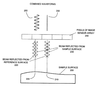
Figure 6 is a diagram schematically illustrating the variation of light
5
CA 02836157 2013-12-11
intensity between pixels adjacent to the pixel shown in Figure 5.
Figure 7 is a flowchart illustrating an example method of calculating a
spatial profile based on a calculation of intensity variance.
Figure 8 is a block diagram illustrating an example computing system for
performing selected embodiments.
Figure 9 shows the variance of the light intensity calculated for pixels
adjacent to the pixel shown in Figure 5, plotted as a function of scanning
position.
Figure 10 is a smoothed version of the image shown in Figure 3, after the
application of a 5x5 pixel unidirectional median filter.
Figure 11 is an image showing the computed variance of each pixel in
Figure 10.
Figure 12 a topography image of a paper surface obtained by associating
the peak variance positions with the zero optical path length position.
Figure 13 is a smoothed topography image based on the image shown in
Figure 12.
Figure 14 is a 3D view of the smoothed topography image from Figure 13.
Figure 15 is a line profile of a location on the topography image from
Figure 13.
DETAILED DESCRIPTION
Various embodiments and aspects of the disclosure will be described with
reference to details discussed below. The following description and drawings
are
illustrative of the disclosure and are not to be construed as limiting the
disclosure.
6
CA 02836157 2013-12-11
Numerous specific details are described to provide a thorough understanding of
various embodiments of the present disclosure. However, in certain instances,
well-known or conventional details are not described in order to provide a
concise discussion of embodiments of the present disclosure.
As used herein, the terms, "comprises" and "comprising" are to be
construed as being inclusive and open ended, and not exclusive. Specifically,
when used in the specification and claims, the terms, "comprises" and
"comprising" and variations thereof mean the specified features, steps or
components are included. These terms are not to be interpreted to exclude the
presence of other features, steps or components.
As used herein, the term "exemplary" means "serving as an example,
instance, or illustration," and should not be construed as preferred or
advantageous over other configurations disclosed herein.
As used herein, the terms "about" and "approximately", when used in
conjunction with ranges of dimensions of particles, compositions of mixtures
or
other physical properties or characteristics, are meant to cover slight
variations
that may exist in the upper and lower limits of the ranges of dimensions so as
to
not exclude embodiments where on average most of the dimensions are satisfied
but where statistically dimensions may exist outside this region. It is not
the
intention to exclude embodiments such as these from the present disclosure.
In conventional two-beam interferometry for the topographic measurement
of a surface profile, an incident light beam is divided into two beams of
equal
intensity, where one beam is directed onto a reference mirror and the other
beam
7
CA 02836157 2013-12-11
is directed onto the sample surface, and optical path difference (the
difference in
optical distances) between the two reflected beams is determined based on the
measured interferogram. An interferogram at a particular location can be
acquired by recording light intensity of the combined beam while varying the
optical path difference of two beams, which is used for determining the
relative
height of the sample surface at this location.
When applied to diffusively reflective surfaces, such as paper or paper-like
materials, the intensity of the light beam reflected from the surface is much
weaker than the reference beam. The interferogram is therefore much weaker
than that obtained for specular or near-specular reflecting surfaces, such as
polished metals, and an interferogram with a clearly identifiable peak is not
observed. Accordingly, such diffusively reflective surfaces are problematic
for the
conventional scanning white light interferometry analysis method, which
requires
a relatively high contrast interferogram.
A conventional scanning white light interferometry surface profile
measuring apparatus is shown in Figure 1. Microscope 101 includes Mirau
interferometer 2, beam splitter 8, epi-illuminator 6, tube lens 9, projective
lens 10,
polarizer 7, polarizer analyzer 12, and 2D CCD image sensor array 13. Mirau
interferometer 2 is supported by piezoelectric transducer 4, and includes
reference mirror 2A on glass plate support 2B, beam splitter 2C, and objective
lens 2D. The piezoelectric transducer is mounted on the microscope nosepiece
4. The vertical position of Mirau interferometer 2 (or Z position, scan
position) is
controlled by PZT controller 14, which receives instructions from computer 5
and
8
CA 02836157 2013-12-11
sends back the current position of PZT to computer 5.
White light from broadband light source 1 irradiates surface 3 of the
sample. The beam reflected from surface 3 and the beam reflected from the
reference mirror 2A propagate through Mirau interferometer 2 and form
interference beam 11. Interference beam 11 passes through beam splitter 8,
polarizer analyzer 12, tube lens 9 and projection lens 10, forming an
interference
image on the sensor plane of image sensor 13. The image is detected by image
sensor 13 and recorded by computer 5 for display and/or analysis. As the
interferometer is moved along the vertical (z) direction by piezoelectric
transducer 4, the intensity of the light detected at a pixel of image sensor
13 will
vary in accordance with the change in the interference fringes, producing an
interferogram.
Figure 2(a) shows an interferogram (for one pixel in a 2D array) obtained
using the aforementioned apparatus for the measurement of a smooth surface
(the experimental implementation of the apparatus included a 10X Mirau
interferometer microscope objective, a 50W halogen lamp, a 100um range PZT
scanner, and a CCD digital camera). A coherence peak occurs at the position
along the scan path Z of zero optical path difference, where L1 equals to L2
in
Figure 1. Since different locations on the sample surface have different
relative
heights, these locations will have coherence peaks at different scan positions
along the scan path. The surface profile data can be generated using the
relative
positions of the coherence peaks of different locations of the sample surface.
The interferogram shown in Figure 2(a) may be processed in order to
9
CA 02836157 2013-12-11
determine the surface height. An example method of processing the
interferogram is as follows. The interferogram is rectified to generate the
waveform shown in Figure 2(b). The rectified waveform is then smoothed into
the
waveform shown in Figure 2(c). The height in this location is determined from
the
peak position of the smoothed waveform, for example, as disclosed in US Patent
Nos. 7,119,907, 5,133,601, or, for example, by fitting the interferogram with
an
envelope function for peak position determination, as disclosed in US Patent
No.
7,199,907. According to such methods, an interferogram (as shown in Figure
2(a) must be obtained at each pixel base on which the optical path difference
may be possibly determined.
When using scanning white light interferometry for the measurement of
surfaces with high spectral reflection, clear interference fringe patterns are
formed and may be captured by an image sensor with high contrast, as
illustrated in Figure 2(a). Unfortunately, as noted above, this method of
processing an interferogram from white light is typically problematic for
diffusely
reflective surfaces. Indeed, when measured on surfaces for which spectral
reflectivity is low, such as paper surfaces, clear interference fringe
patterns are
generally not observed, and interference may only be formed in some particular
locations on the surface, where some degree of specular reflection occurs.
This failure of conventional scanning white light interferometric methods
for diffusely reflective surfaces is demonstrated in Figure 3, which plots a
2D
interferogram based on measurements made of a paper surface (the paper was
a sheet of commercial office copying paper). Although some interference
CA 02836157 2013-12-11
features are visible in the image at several locations, the signal-to-noise
ratio of
the interferogram for most of the area is too low to compute the location of
the
surface.
Figure 4 shows an interferogram measured at a location on the paper
surface where some specular reflection was present, for which moderate fringe
contrast was visible. The interferogram was obtained by plotting the light
intensity
of a selected pixel at each scanning position along the scanning direction (in
this
case, the optical axis of the interferometer). Interference fringes
corresponding to
an optical path difference of zero are visible in the interferogram at a scan
position of approximately 13 microns.
Figure 5 shows an interferogram at another pixel where the reflection was
predominately diffuse in character. Unlike the interferogram shown in Figure
4,
this interferogram exhibits very low fringe visibility, with no discernible
peak. The
lack of a discernible peak precludes the determination of the optical path
difference, and thus the surface profile, at this location. This Figure
demonstrates
how interference fringes are not formed at most locations across the surface
area
when using scanning white light interferometry for the measurement of
diffusely
reflective surfaces, such as paper or paper-like materials.
The surface of paper essentially consists of pulp fibers. Accordingly, both
a paper surface and a natural fiber surface are not perfectly flat at any
scale.
While scanning via white light interferometry, when the optical path
difference of
one pixel of the paper surface image is zero (phase difference =0), the
optical
path differences of adjacent pixels are usually different due to the rough
nature of
11
CA 02836157 2013-12-11
the fiber surface.
This local variation in the optical path difference is schematically
illustrated
in Figure 6, where interference from light reflected from positions 205 and
210 of
sample surface 200 is shown. Positions 205 and 210 correspond to different
pixels of image sensor array 240. At position 205, reflected reference beam
220
and reflected sample surface beam 230 are in phase and produce combined
waveform 250 having a net signal. At nearby position 210, however, the surface
profile has changed on the scale of the wavelength of the light, and reflected
reference beam 220 and reflected sample surface beam 230 are out of phase,
destructively interfering such that combined waveform 255 is minimized. As a
result, the interference light intensity detected on adjacent pixels of the
image
sensor varies dramatically, even though the reflectance of the sample surface
at
corresponding locations is similar.
In some embodiments of the present disclosure, this local variation in the
intensity of the combined waveform, when determined for different pixels, can
be
exploited in order to determine the position of zero optical path difference
in a
computationally efficient manner. This can be achieved by utilizing the
variance
in the detected light intensity within a region neighbouring a given pixel.
When
the dependence of this variance, for a given pixel, is considered as a
function of
the scanning position, the variance has been found to exhibit a peak value
corresponding to the position at which the optical path difference equals
zero.
This method is less complex and less computationally intense that other
methods
of processing interference data from diffusely reflective surfaces.
12
CA 02836157 2013-12-11
Figure 7 shows a flow chart describing an example embodiment for
calculating the surface topology of a diffusively reflecting surface, such as
a
paper surface, based on a series of images obtained using a scanning white
light
interferometry apparatus. In step 300, a white light scanning interferometer
is
employed to obtain a collection of images along a scanning direction. In step
310, for each image, a variance is calculated for each pixel, where the
variance
of a given pixel is obtained by including image values for a set of
neighbouring
pixels (optionally including the image value of the given pixel), thereby
providing
a variance value for each pixel in each image. The scanning position
associated
with the maximum variance of each pixel is then determined in step 320. The
position of zero optical path difference is then determined to be the scanning
position corresponding to the maximum variance, as shown in step 330. A
surface profile may then be computed from the zero optical path difference
positions determined for the pixels in step 340.
The surface profile may be plotted as a topography image. In some
embodiments, the surface profile and/or the topography image may be smoothed
to remove noise. The surface profile data may be employed to calculate the
surface roughness.
Prior to calculating the position of zero OPD, the initial images in the
lateral direction may be smoothed to remove high spatial frequency noise, for
example, using a median filter or a Gaussian filter.
The variance of light intensity can be calculated using any of several
known algorithms, such as derivative based, histogram-based, statistical based
13
CA 02836157 2013-12-11
algorithms [1, 2]. The number of pixels sampled for the variance calculation
is not
limited to 5x5 (as shown in the examples), and may take on a wide range of
values and configurations depending on the application and the surface that is
being measured. Although several example embodiments described herein refer
to the calculation of a two-dimensional variance within an image, it is to be
understood that the variance may also be computed using intensity data from
neighbouring pixels in one or more adjacent images, such that the variance is
computed based on a local three-dimensional data set.
To determine the peak in variance at a location, the first order derivative of
the variance series in the scan direction is calculated, for example, using
the
Savitzky-Golay filter. The peak in variance is then determined where the value
of
the first order derivative crosses zero. The scanning position at the peak as
well
as the variance at the peak is recorded. If there is no zero crossing of the
derivative found, the point may be considered as an outlier and/or invalid. If
the
variance at the peak is less than a certain value, which is sample dependent,
the
point may also be considered to be an outlier and/or invalid. The location of
OPD
of all invalid points may be interoperated from the nearest valid points
surrounding it using linear or polynomial interpolation. The constructed
topography image may be smoothed using a low pass filter to remove high
frequency noise.
Although the example embodiments disclosed above pertain to the
determination of the surface profile on a per-pixel basis, it is to be
understood
that the method need not be performed with single-pixel resolution. For
example,
14
CA 02836157 2013-12-11
in other implementations, each variance measure, and each position of zero
optical path difference, may be determined for a plurality of pixels. For
example,
the variance may be calculated by selecting a group of pixels (for example,
four
pixels), and computing the variance among pixels that neighbor this group of
pixels. This would result in a lower resolution surface profile, but would
increase
the computational efficiency of the method and decrease the processing time of
a
given surface profile determination.
The embodiments described herein may be employed for the
measurement of rough surfaces that have low spectral reflected intensity,
without
the need to perform complex mathematical analyses of low coherent interference
fringes. In some example implementations, the methods disclosed herein may be
employed for measuring surfaces with an RMS average roughness of
approximately one micron or greater.
The embodiments disclosed herein may be employed for the
measurement of surface topology of a wide variety of materials having
different
surface characteristics. In some embodiments, the preceding methods may be
employed for the measurement of measuring paper, paperboard and paper-like
materials that have low spectral reflection and low interferogram contrast. In
other non-limiting examples, the sample may be non-coated paper made of
natural pulp fibers, coated paper, textiles, woven and nonwoven materials,
plastics, rubber, ceramics, wood, engineered wood products, polymer and
polymer composite materials, and biological tissues.
Embodiments provided herein may provide improved sensitivity to off-axis
CA 02836157 2013-12-11
measurements and/or misalignments, as the methods disclosed herein may be
less sensitive to surface orientation (when compared to methods that depend on
specular reflection), since the diffuse reflection will be more isotropic in
nature.
The method proposed can also be combined with the conventional
coherence scanning interferometry data processing method to improve the
accuracy in surface topography construction. The scanned images may be
processed to find out the surface location where clear interference fringe
patterns
are observed. These points may be compared with the values calculated using
the peak of variance method. If the values of two methods disagree, the values
from the conventional method may be treated as valid points. Valid points
could
be used for interpolating to replace the values of invalid points.
In some embodiments, the outliers in the variance data may be identified
and treated as invalid points prior to final topography construction. For
example,
outliers may be identified by comparing the peak variance value (or the
inferred
surface height) to a threshold. The surface location of the outlier may be
interpreted from surrounding valid points, for example, using interpretation
such
as linear or polynomial interpolation, or using a median filter. Examples of
outliers include points where no zero crossing in the first order derivative
of
vertical variance series occur, points with very low variance peak values, and
insolated points on the variance peak map caused by impulse noise.
It will be understood that the methods disclosed herein may find
application for most natural materials, as their surfaces are rough in a large
scale
range, and therefore the interferogram intensity usually varies from location
to
16
CA 02836157 2013-12-11
location. For materials having an ultra-smooth surface, as long as the surface
is
aligned to record the scanning beam, the interferogram intensity variation
still
occurs, and the methods provided herein may be employed.
The ability of the present methods to perform measurements in the
presence of surface discontinuities (or high slopes) may depend on the numeric
aperture of the objective lens used. For example, when the workpiece has
features with large local slopes on the surface, and the specular reflection
dominates, the face of the slope acts as a mirror reflecting the light outside
of the
objective lens. However, as in the case of materials having a diffusely
reflecting
surface, a substantial amount of light may be reflected towards the objective
lens, and thus the maximum measurable slope may exceed that of conventional
methods.
Figure 8 illustrates a block diagram of an example computing system 400
that may be employed to perform various methods according to the embodiments
provided in the present disclosure. Control and processing unit 425, which is
described in further detail below, may be employed for the processing of
images
obtained by the white light scanning interference apparatus, and optionally
for the
control of the white light scanning interference apparatus. For example,
computer
5 in Figure 1 may be substituted with computing system 400 for implementing
various embodiments disclosed herein.
Some aspects of the present disclosure can be embodied, at least in part,
in software. For example, the method steps disclosed in Figure 7, or
variations
thereof as per alternative and/or additional embodiments, may be performed by
a
17
CA 02836157 2013-12-11
processor according to instructions provided in software or firmware. That is,
the
techniques can be carried out in a computer system or other data processing
system in response to its processor, such as a microprocessor, executing
sequences of instructions contained in a memory, such as ROM, volatile RAM,
non-volatile memory, cache, magnetic and optical disks, or a remote storage
device. Further, the instructions can be downloaded into a computing device
over
a data network in a form of compiled and linked version. Alternatively, the
logic to
perform the processes as discussed above could be implemented in additional
computer and/or machine readable media, such as discrete hardware
components as large-scale integrated circuits (LSI's), application-specific
integrated circuits (ASIC's), or firmware such as electrically erasable
programmable read-only memory (EEPROM's) and field-programmable gate
arrays (FPGAs).
Figure 8 provides an example implementation of control and processing
unit 425, which includes one or more processors 430 (for example, a
CPU/microprocessor), bus 432, memory 435, which may include random access
memory (RAM)and/or read only memory (ROM), one or more internal storage
devices 440 (e.g. a hard disk drive, compact disk drive or internal flash
memory),
a power supply 445, one more communications interfaces 450, external storage
455, a display 460 and various input/output devices and/or interfaces 465.
Although only one of each component is illustrated in Figure 8, any
number of each component can be included in the control and processing unit
425. For example, a computer typically contains a number of different data
18
CA 02836157 2013-12-11
storage media. Furthermore, although bus 432 is depicted as a single
connection
between all of the components, it will be appreciated that the bus 432 may
represent one or more circuits, devices or communication channels which link
two or more of the components. For example, in personal computers, bus 432
often includes or is a motherboard.
In one embodiment, control and processing unit 425 may be, or include, a
general purpose computer or any other hardware equivalents. Control and
processing unit 425 may also be implemented as one or more physical devices
that are coupled to processor 430 through one of more communications channels
or interfaces. For example, control and processing unit 425 can be implemented
using application specific integrated circuits (ASICs). Alternatively, control
and
processing unit 425 can be implemented as a combination of hardware and
software, where the software is loaded into the processor from the memory or
over a network connection.
Control and processing unit 425 may be programmed with a set of
instructions which when executed in the processor causes the system to perform
one or more methods described in the disclosure. Control and processing unit
425 may include many more or less components than those shown.
While some embodiments have been described in the context of fully
functioning computers and computer systems, those skilled in the art will
appreciate that various embodiments are capable of being distributed as a
program product in a variety of forms and are capable of being applied
regardless of the particular type of machine or computer readable media used
to
19
CA 02836157 2013-12-11
actually effect the distribution.
A computer readable medium can be used to store software and data
which when executed by a data processing system causes the system to perform
various methods. The executable software and data can be stored in various
places including for example ROM, volatile RAM, non-volatile memory and/or
cache. Portions of this software and/or data can be stored in any one of these
storage devices. In general, a machine readable medium includes any
mechanism that provides (i.e., stores and/or transmits) information in a form
accessible by a machine (e.g., a computer, network device, personal digital
assistant, manufacturing tool, any device with a set of one or more
processors,
etc.).
Examples of computer-readable media include but are not limited to
recordable and non-recordable type media such as volatile and non-volatile
memory devices, read only memory (ROM), random access memory (RAM),
flash memory devices, floppy and other removable disks, magnetic disk storage
media, optical storage media (e.g., compact discs (CDs),digital versatile
disks
(DVDs), etc.), among others. The instructions can be embodied in digital and
analog communication links for electrical, optical, acoustical or other forms
of
propagated signals, such as carrier waves, infrared signals, digital signals,
and
the like.
The method proposed can also be used with other types of optical surface
topography measurement systems, such as, but not limited to, focus variation
instruments, point autofocus instruments, imaging devices such as cameras,
CA 02836157 2013-12-11
imaging confocal microscopy, endoscopic imaging devices, and other optical
systems and devices.
The following examples are presented to enable those skilled in the art to
understand and to practice embodiments of the present disclosure. They should
not be considered as a limitation on the scope of the present embodiments, but
merely as being illustrative and representative thereof.
EXAMPLES
The aforementioned embodiments are demonstrated, by way of example,
in Figure 9, which shows the dependence of the lateral variance of light
intensity
distribution along the scanning direction for the same pixel as shown in
Figure 5.
The lateral variance was calculated for each scanning position by selecting a
set
of pixels neighbouring a given pixel (optionally including the given pixel)
and
computing the variance of the intensities recorded among the set of pixels. In
other words, the variance for a given pixel was determined by applying a
variance filter to a region surrounding the pixel. In the example
implementation
shown in Figure 9, the variance was calculated on a 5x5 array of pixels around
the selected pixel. As can be seen in Figure 9, a peak in the variance values
is
clearly observable. The position for which the optical path difference equals
zero
was determined based on the scanning position corresponding to the peak
variance. The positions of zero optical path difference were then employed to
determine the surface profile, which may be plotted as a topography image.
In the present example, the measured interference images were
21
CA 02836157 2013-12-11
smoothed prior to determining the variance and identifying the variance peak
locations. The interference images were smoothed via a median filter, which
may
be a unidirectional filter, by which the center pixel of a given region (e.g.
5x5 pixel
region) of an image may be replaced by the median of the pixels within this
region. The smoothed image of Figure 3, according to a 5x5 pixel region
unidirectional median filter, is shown in Figure 10.
Figure 11 shows the result of the application of the variance filter to the
smoothed image of Figure 10, where the variance filter involved a 5x5 region.
Figure 12 is a topography image obtained after identifying the position
corresponding to the variance peak for each pixel, and equating this position
to
the zero optical path difference position.
The topography image was subsequently smoothed to produce the image
shown in Figure 13. The smoothing algorithm involved the convolution with a
Gaussian function:
1
G(x, y) = 2e 262 , (1)
27zrr
with a radius of 8 pixels [3]. A three dimensional plot of the surface profile
is
shown in Figure 14, clearly revealing a rich surface structure on the micron
scale.
Figure 15 shows a line profile of the height map across the x-direction at a
value of Y=256, which can be employed for calculating RMS roughness.
The specific embodiments described above have been shown by way of
example, and it should be understood that these embodiments may be
susceptible to various modifications and alternative forms. It should be
further
22
CA 02836157 2013-12-11
understood that the claims are not intended to be limited to the particular
forms
disclosed, but rather to cover all modifications, equivalents, and
alternatives
falling within the spirit and scope of this disclosure.
REFERENCES
1. Sun, Y., Duthaler, S., and Nelson, B.J., "Autofocusing in Computer
Microscopy: Selecting the Optimal Focus Algorithm", 65: 139-149,
Microscopy Research and Technique, (2004).
2. Frans C.A. Groen, Ian T. Young, and Guido Ligthart, "A Comparison of
Different Focus Functions for Use in Autofocus Algorithms" 6:81-91,
Cytometry,(1985)
3. Shapiro, L. G. & Stockman, G. C: "Computer Vision", page 137, 150.
Prentice Hall, 2001.
23