Note: Descriptions are shown in the official language in which they were submitted.
CA 02846461 2014-02-25
WO 2013/030064
PCT/EP2012/066339
LAYERED MANUFACTURING OF FREE-FORM MULTI-MATERIAL MICRO-
COMPONENTS
Field of the invention
The present invention relates to layer manufacturing, more particularly to a
method for additive layer manufacturing of objects comprised of more than
one material with free-form capability for all included materials.
The invention deals with a method to fabricate objects by starting with a
virtual 3D model (CAD- model) and using this information to add material in
a controlled manner to shape the object. These types of methods are
commonly referred to by a number of terms for example rapid prototyping,
free-form fabrication, layer manufacturing and additive manufacturing. 3D-
printing is one method that belongs to this group. Since objects with very
complex shapes can be described by a set of planar layers this method
makes it possible to fabricate any desired shape within the precision of the
actual implementation of these layered manufacturing methods.
Background Art
3D-printing is a method where a powder layer is distributed on a surface. An
inkjet printer is used to distribute a binder on the surface to create a
temporary bond between the particles. The binder is dried and the process
is repeated until a powder bed containing an object bound together with the
binder is created. The lose powder is rinsed or cleared from the object and
the object is then sintered. The boundaries between the original powder
layers disappear and a solid object is created.
Advantages with 3D printing compared to other layer manufacturing
methods are the high speed, no need to build support structures and that
the final object is homogenous without residual stresses. The high speed
comes from the deposition of the powder layer in one step and that the
CA 02846461 2014-02-25
WO 2013/030064 2 PCT/EP2012/066339
binder can be deposited with several nozzles simultaneously. Other
methods that can build objects by dispensing at each point or use a single
laser or electron beam spot for selective solidification are inherently slower
since they can only build at one point at a time. The powder bed supports
the structure making it possible to build structures containing arches without
building a separate support structure that has to be removed in a later step.
The powder can be deposited without density gradients and this secures
that the sintering done in a separate stage can create homogenous object
without differential shrinkage.
In the original 3D-printing invention (Cima US6146567) the powder was
applied on the surface by spraying a suspension. In a later invention by
Fcubic the powder is spread in the dry form to create a layer (Fcubic
W003055628). The latter method is very fast but it is limited to coarser
powders with approximately 10-20 pm particle size that can be spread
homogenously in the dry state. Finer powders, this includes most sinterable
ceramic powders and hard metal powders, are impossible to spread in the
dry state in a homogenous thin layer due to van der Waals attraction that
inhibits the flow of dry small particles.
Microsystems are increasingly used to make products smarter, that is to add
new functionally to products. They are for example used in products like
solar cells, batteries, OLED, microwave components, lab-on-a chip and high
temperature sensors, vehicles and kitchen appliances. Microsystems can
contain sensors that sense (acceleration, radiation, force, pressure,
moisture, chemical environment etc) they can also contain actuators based
on electrostatic, magnetostrictive, piezoelectric and other principles.
To date it has not been possible to use layered manufacturing to directly
fabricate Microsystems packaging with true 3D structures. Available
methods such as LTCC (low temperature cofired ceramics) can only supply
flat substrates where the electronic connection (vias) have to be placed
perpendicular to the layers. This often makes it necessary to combine LTCC
structures with other 3D-structures manufactured separately. Using additive
and direct manufacturing to build the package would create a competitive
CA 02846461 2014-02-25
WO 2013/030064 3 PCT/EP2012/066339
advantage. Developing of integrated electronic chips is a very efficient
streamlined production process done by silicon foundries. The packaging is
however not standardized in the same way. Packaging is often the major
cost in production of Microsystems. Further design, fabrication and testing
of packaging are very time consuming processes.
The electrical interconnects for Microsystems are built with an insulating and
an electrically conducting material. For some applications other materials
are required to build resistors and to modify the dielectric properties. For
optical interconnects, other material combinations are required to build
waveguides. This requires that the fabrication process can build with and
integrate several materials. This has not been possible in previously
available methods for layered manufacturing.
Summary of the Invention
In view of the above-mentioned and other drawbacks of the prior art, a
general object of the present invention is to provide manufacturing of 3D-
objects containing several materials with additive layered manufacturing.
The invention enables efficient production of objects consisting of a powder
based material (such as a ceramic, glass, hybrid, intermetallic, hard metal or
metal material) but with additions of one or more secondary materials (such
as a ceramic, glass, hybrid, intermetallic, hard metal or metal material). The
secondary material can be integrated with freeform capability.
According to an aspect of the present invention, it relates to a method for
additive layer manufacturing of objects comprised of more than one material
with free-form capability for all included materials, which method comprises
providing a flat substrate as a platform for building the object,
hydrophobizing selected parts of a flat substrate by applying a hydrophobic
solution, spreading a water-based powder suspension comprised of
particles with a size below 5 pm in a layer with a thickness below 50 pm,
applying a binder to the parts of the powder layer that should be retained in
the shaped powder body, applying one or more secondary materials as
powder suspensions or powder pastes to the gaps in the layer created by
CA 02846461 2014-02-25
WO 2013/030064 4 PCT/EP2012/066339
the hydrophobic repulsion of the water-based suspension, repeatedly
adding powder layers, hydrophobic areas, binders and secondary materials
as above to build a powder body of the desired shape and size, rinsing or
clearing the object from lose powder and removing the object from the
support, and performing thermal treatment to remove the binder and sinter
the powder object to a solid body.
According to various exemplifying embodiments, a flat support is provided
as a platform to build the object. A fine powder is deposited as a water-
based suspension on the support using a slot die, doctor blade or extrusion
method. A temporary binder is used to bind parts of the layer that should be
included in the final shaped object. The water dries off rapidly from the
concentrated suspension to solidify the layer. Several layers are deposited
on top of each other to build the object with addition of a binder. A
hydrophobic material is deposited selectively on each powder layer to
create gaps in the next layer. The hydrophobic parts repel the water-based
suspension. These gaps are filled with secondary materials using inkjet
printing or dispersing. The deposition of powder layers and secondary
materials is repeated with a desired number of layers. When the entire
object is built, the lose powder, e.g. powder not bound together with the
temporary binder, is rinsed or cleared from the object. The object is
removed from the support prior to or after the rinsing or clearing from lose
powder. The object is then heated to remove the temporary binder followed
by further heating to sinter the object to a solid component containing
several materials
In this way structures of secondary material with an arbitrary shape can be
included in the object. These structures can for example be used to build 3D
vias (electrically, optically or thermally conducting lines of an arbitrarily
shape and direction) in an insulating or refractive matrix.
Generally, other objectives, features, and advantages of the present
invention will appear from the following detailed disclosure, from the
attached dependent claims as well as from the drawings are equally
possible within the scope of the invention.
CA 02846461 2014-02-25
WO 2013/030064 5 PCT/EP2012/066339
Brief Description of Drawings
Embodiments of the invention will now be described, by way of example,
with reference described exemplifying embodiments, experiments and to the
accompanying drawings, wherein:
Fig. 1 is a schematic view illustrating the addition of binder to shape a
structure and removal of lose powder according to an embodiment of the
present invention.
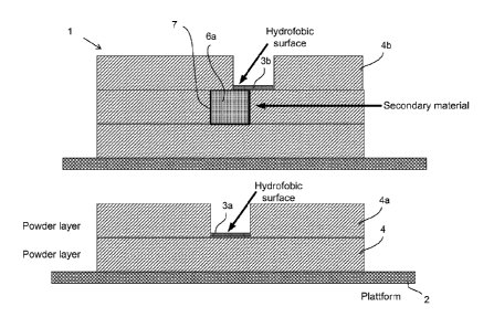
.. Fig. 2 is a schematic view illustrating the principle of creating gaps in
layer
to be filled with a secondary material according to an embodiment the
present invention.
Fig. 3 is a schematic view of a contact pattern according to an embodiment
of the present invention.
Fig. 4 is a schematic view of an exemplifying embodiment according to the
present invention.
Fig. 5 is a schematic flow chart of an embodiment of the method according
to the present invention.
It should be understood that the drawings are not true to scale and, as is
readily appreciated by a person skilled in the art, dimensions other than
those illustrated in the drawings are equally possible within the scope of the
invention.
Detailed Description of Embodiments of the Invention
According to various embodiments, the invention can be used for producing
packaging for Microsystems where the ceramic acts as an insulator and the
secondary material is used to, or forms, 3D conductor lines or 30 vias. The
.. fine powder used in this method makes it possible to be used, or enables,
for building components with small feature size, high precision, and/or
demand for high precision. Other intended uses for this method is to build
optoelectronic systems, nnicrofluidic systems, small mechanical precision
parts, grinding tools, dental objects or medical implants. Microsystems
.. formed according to various embodiments according to the invention may
CA 02846461 2014-02-25
WO 2013/030064 6 PCT/EP2012/066339
advantageously be used to make products smarter, that is to add new
functionally to products.
The invention builds on the concept of 3D-printing. But instead of spreading
or spraying a dry powder the powder layer is added as a concentrated
suspension in water. The suspension is applied in a thin layer using a slot
die, a doctor blade, extrusion deposition or other techniques for spreading
the suspension. This is different from spraying were the ceramic or metal
has to be in a very dilute suspension in order to have a viscosity to pass
through the spraying nozzle. With application of a suspension with a slot die
it is possible to add a very thin powder layer (1-50 pm) in a precisely
controlled manner from a highly concentrated suspension. The term highly
concentrated is here used to describe a suspension near the theoretical
random close packing concentration. The highly concentrated suspension
rapidly solidifies as it only takes the removal of a minute quantity of water
to
convert it into a solid. A binder is then printed on parts of the layer that
should remain in the final body.
The addition of a binder to shape the structure by removing lose powder by
rinsing or clearing is illustrated by Figure 1. The principle of creating gaps
in
layers to be filled with a secondary material is illustrated by Figure 2.
The material added as layers can be a ceramic but it is also possible to
spread layers of other fine powders such as glass, hybrid materials,
cemented carbides, internnetallics or metals. The requirement is that the
powders have a low particle size, such as <5 pm, so that they can be
dispersed with reduced, or without, sedimentation but also to be able to
work with thin layers to make it possible to form small shapes with high
precision. The powders may further be dispersed in water with reduced, or
without, significant reaction between the fine powder and the water.
Furthermore, according to the method, the powder may be sintered to a
dense final material. For this purpose, fine non-agglomerated powders with
sintering ability are utilized, wherein the particle size requirement depends
on the actual type of material. For high performance ceramics a particle size
below 1 pm may be utilized.
CA 02846461 2014-02-25
WO 2013/030064 7 PCT/EP2012/066339
3D-printing processes can be arranged to create internal cavities (holes or
channels) in a component as long as they are connected to the surface of
the component and can be rinsed or cleared from lose powder after the
component is created. To fill created cavities with a secondary material after
manufacturing of the entire component is difficult and unpractical. To be
able to add a second material inside the component may be useful, or
necessary, in order to create the space for it as the layer is created.
To use mechanical drilling or laser machining to create cavities in each layer
is possible but would cause emission of chips or other debris. This would be
very difficult to remove and would destroy a process that aims at small
structures created with high precision and high quality.
Instead of machining a hydrophobic liquid is printed selectively on part of a
layer. When the next layer is added the hydrophobic areas repel the water-
based powder suspension causing a gap (hole of cavity) in the layer where
a second (or third or fourth material can be added). The hydrophobic liquid
can for example comprise, or consist of, hydrocarbons (alkanes, oils fats),
fluorocarbons or silicones.
Since the cavities are created layer by layer they can be filled layer by
layer
with a paste of a secondary material using dispensers, inkjet printing or
other application methods. The filling of cavities with a dispenser (done at
one point a time) is a slower process than the inkjet printing of the binder
(done with an array of nozzles) but in most applications the area that has to
be filled is only a small portion of the entire section of the component. In
this
way the main advantage of depositing and solidifying entire layers rapidly is
maintained.
This process enables the creation of 3-dimensional via holes (3-D
conductive connections or optical vias) inside of the component or to
integrate other 3D structures of a second material in the structure. The
added materials may be chosen or be adapted to be compatible with the
sintering procedure. This problem, however, is solved for example in the
CA 02846461 2014-02-25
WO 2013/030064 8 PCT/EP2012/066339
commercially available LTCC technology (low temperature co fired ceramics
for electronics applications).
According to an embodiment, the process can also be used with adding a
sacrificial material as secondary material in the gaps created by the
hydrophobic areas. The sacrificial material is chosen to temporary fill the
gaps but to disappear during heat treatment prior to sintering or during the
early stages of sintering. This can be used to include channels, closed
channels and/or cavities in the component. Since these cavities are not
filled with permanent secondary material they do not have to be connected
to the outside surface of the body. The sacrificial material breaks
down/evaporates through the pores of object before they are sealed during
sintering. One example of a sacrificial material is graphite that oxidizes to
form carbon dioxide if the object is heated in air during heat treatment.
Another example of a sacrificial material is a wax that melts and evaporates
during heat treatment. Rinsing or clearing of small channels or small cavities
is often difficult and time consuming even if the channels or cavities are
open to the surface of the object.
It is also possible with this method to add planar conductor lines by inkjet
with a conductive metallic ink before the next ceramic layer is added in a
similar manner as done in the LTCC technology.
For example, the method enables fabrication of ceramic packaging (or
ceramic interconnects) for a wide range of Microsystems. To add functional
materials and to connect this material by electric conductors makes it
possible to add sensors or actuators. Adding conductor lines, resistors,
inductances and capacitances and connection points for electronic chips
opens for smart system integration. Microsystems may for example be used
in products like solar cells, batteries, OLED, microwave components, lab-
on-a chip and high temperature sensors, vehicles and kitchen appliances.
Microsystems can further contain sensors that sense (acceleration,
radiation, force, pressure, moisture, chemical environment etc) they can
also contain actuators based on electrostatic, nnagnetostrictive,
piezoelectric
and other principles. Microsystems can also contain cavities that form
CA 02846461 2014-02-25
WO 2013/030064 9
PCT/EP2012/066339
waveguides for light and microwaves, as well as channels for transport of
fluids. Microsystems formed according to the method may also contain
optical waveguides.
The high precision and capability to build complex features and integrate
secondary materials gives the possibility to fabricate small complex
machining tools or medical implants as well as dental products. The method
also gives the possibility to create channels and cavities with internal
metallization. Such structures can be used as wave guides in microwave
applications. For high frequency microwave (THz or near THz) microstrip
connections needs to be replaced with wave guides. These waveguides
(metalized channels) need to be of high precision and with low surface
roughness to avoid losses. Such high precision and low surface roughness
can be manufactured with this method.
Example 1
In a simple model experiment a doctor blade casting station was used
instead of slot die for manual application of layers. On a plate of sintered
alumina a metallic pattern was screen printed. The pattern consisted of
straight conductor lines in different dimensions finished by a contact point,
Figure 3. Printing was done with a silver paste to have good electrical
conduction.
The plate with the conductor was placed in the casting station. An alumina
suspension (40 vol /0 AKP 30, Sumitomo Chemicals), in water with a
dispersing agent (0,35 % Dolapix PC21) was cast with a doctor blade with
80 pm gap. This casting created a film with fine alumina powder on the
plate.
Holes for vias were created by dispensing of a hydrophobic liquid. The
hydrophobic liquid was a fluorocarbon based liquid. On areas where the
hydrophobic liquid was applied the alumina water-based suspension did not
wet and thus it avoided those areas. Holes are created that penetrate the
dry alumina powder layer.
CA 02846461 2014-02-25
WO 2013/030064 10 PCT/EP2012/066339
A new layer of conductors was screen printed on top of the dried ceramic
layer. The second layer conductive pattern is displaced so that the first
layer
can connect through the contact point. Silver paste penetrates through the
created holes and connects the first layer with the second layer, thus
establishing a via connection.
Connection was confirmed by measuring a short circuit between the upper
and lower layer endpoints that are shown in Figure 4. The current has gone
.. alternating through the upper and lower layer through six vias.
Example 2
A machine for layer manufacturing was built. It consists of a table with
linear
actuators (NSK and HIWIN) that can move a stage in x-y-z directions. The
movable stage is controlled with a PLC controller (Beijer).
The movable stage is fitted with a slot die (Premier Dies) fed by a ceramic
suspension under pressure with a precision pump (such as a precision gear
pump). The ceramic suspension is similar to example 1 but the solids
concentration was adjusted to a viscosity suitable for the slot die.
Inkjet heads (HP) with a drive electronic (Megatech Electronic) was fixed to
the stage to be able to print both a temporary latex binder and a
hydrophobic liquid.
Dispensers were also fitted to the movable stage and filled with conductive
paste.
A computer was programmed to control the slot die through the PLC and to
transfer printing information to drive printing electronic for each layer. The
movable stage was then raised before deposition of the next layer.
This machine was used to building 3D conductive vias in ceramic packaging
.. structure.
11
With reference to Fig. 1, Fig. 2 and Fig. 5, embodiment objects 1
manufactured using exemplifying method 11 are illustrated. As shown, the
exemplifying embodiment of the method 11 comprises:
- providing a flat substrate as a platform forming a support 2 for building
the
object 1, indicated by block 12 in fig. 5,
- hydrophobizing selected parts of a flat substrate, such as the powder layer
4, 4a, 4b of water-based powder suspension, or the platform forming the
support 2, by applying a hydrophobic solution, such as 3a or 3b, indicated
by block 13 in Fig. 5;
- spreading a water-based powder suspension 4a or 4b comprised of
particles with a size below 5 (five) pm in a layer with a thickness below 50
(fifty) pm, indicated by block 14 in Fig. 5;
- applying a binder 5 to the parts of the powder layer that should be retained
in the shaped powder body, indicated by block 15 in Fig. 5;
- applying one or more secondary materials 6a as powder suspensions or
powder pastes to the gaps 7 in the layer created by the hydrophobic
repulsion of the water-based suspension, indicated by block 16 in Fig. 5;
- repeatedly adding powder layers 4a, 4b, 4c, etc., hydrophobic areas 3a
and 3b, binders 5a, 5b, and 5c and secondary materials corresponding to
secondary material 6a, as above to build a powder body of the desired
shape and size, indicated by block 17 in Fig. 5;
- rinsing or clearing the object from lose powder and removing the object
from the support 2, indicated by block 18 in Fig. 5; and
- performing thermal treatment to remove the binder and sinter the powder
object to a solid body, indicated by block 19 in Fig. 5.
It is noted that, with reference to Fig. 2, it is illustrated that selected
part of
the powder layer 4a and 4b forms the flat substrate which is/are
hydrophobized by applying a hydrophobic solutions 3a and/or 3b. However,
the hydrophobic solution may also be applied directly on the platform
forming the support 2, wherein the platform forming the support 2 forms the
flat substrate in the hydrophobizing step.
CA 2846461 2019-02-11
CA 02846461 2014-02-25
WO 2013/030064 12 PCT/EP2012/066339
It should be noted that the invention has mainly been described above with
reference to a few embodiments. However, as is readily appreciated by a
person skilled in the art, other embodiments than the ones disclosed above
are equally possible within the scope of the invention, as defined by the
appended patent claims.
It is further noted that, in the claims, the word "comprising" does not
exclude
other elements or steps, and the indefinite article "a" or "an" does not
exclude a plurality. A single apparatus or other unit may fulfill the
functions
of several items recited in the claims. The mere fact that certain features or
method steps are recited in mutually different dependent claims does not
indicate that a combination of these features or steps cannot be used to an
advantage.