Note: Descriptions are shown in the official language in which they were submitted.
1
ASSEMBLY AND INTERCONNECTION METHOD FOR HIGH-POWER LED
DEVICES
Background of the Invention
1. Field of the Invention
This invention relates to LED arrays and, in particular, this invention
relates to LED arrays with interchangeable LED assemblies.
2. Background
High intensity Light Emitting Diode ("LED") devices present great
challenges in designing thermal energy management, optical energy
management, and electrical energy management (interconnection). This is a
particular problem when designing LED light-emitting systems, which focus
high levels of specific wavelength light energy at relatively short distances,
such as 10 mm - 100 mm. These designs require high-density packaging
(mounting) of the LED devices. A method is therefore needed to electrically
interconnect existing LED "package" designs to meet the high density, as
well as electrical energy, management goals. Because of the high intensity
light energy, materials used must withstand the energy emitted at the
particular wavelength of the applicable device or system.
There is then a need for an LED package, which produces high-
intensity radiant energy emitted from a high-density LED array. There is a
CA 2848760 2017-10-10
CA 02848760 2014-03-13
WO 2013/040.453 PCT/US2012/055568
2
particular need for an LED package, which can be quickly and easily repaired
on-site or altered to provide varying wavelengths of radiant energy.
Summary of the Invention
This invention substantially meets the aforementioned needs of the
industry by providing an LED array with easily and quickly replaceable LED
assemblies.
There is provided an LED array comprising a mounting substrate, a
plurality of LED assemblies, a plurality of power connect clamps, and a
plurality of interconnect clamps. The LED assemblies are attached to the
substrate and each have positive and negative electrodes electrically
connected to an LED chip. The power connect clamps connect each of a pair
of terminal LED assemblies to an electrical power source. The power connect
clamps may include a power connect fastener threaded into a power connect
aperture. The power connect fastener may be threaded into an electrical
connector to connect each of the power connect clamps to the power source.
The interconnect clamps connect positive and negative electrodes adjacent
LED assemblies such that the LED assemblies are interconnected in an
electrical series. Each of the interconnect clamps may have a pair of
interconnect fasteners, each of the interconnect fasteners threaded into an
interconnect aperture. The interconnect fastener may be threaded against a
positive or negative electrode to connect and secure the positive and negative
electrodes adjacent LED assemblies into the electrical series.
Brief Description of the Drawinas
CA 02848760 2014-03-13
WO 2013/040453 PCT/US2012/055568
3
Figure 1 is a perspective view of one embodiment of the LED array of
this invention.
Figure 2 is a perspective view of one embodiment of an LED assembly
utilized in the LED array of Figure 1.
Figure 3 is a perspective view of the LED assembly of Figure 2 with a
lens in place covering the LED chip.
Figure 4 is a perspective view of another embodiment of an LED
assembly suitable for use in the LED array of Figure 1.
Figure 5 is a perspective view of a bottom side of a mounting substrate
suitable for use with the LED array of Figure 1.
Figure 6 is a perspective view of a top side of the mounting substrate of
Figure 5.
Figure 7 is a perspective view of one embodiment of a power connect
clamp used in the LED array of Figure 1.
Figure 8 is a perspective view of one embodiment of an interconnect
clamp used in the LED array of Figure 1.
It is understood that the above-described figures are only illustrative of
the present invention and are not contemplated to limit the scope thereof.
Detailed Description
Unless otherwise defined, all technical and scientific terms used herein
have the same meaning as commonly understood by one of ordinary skill in
the art to which this invention belongs. Although methods and materials
CA 02848760 2014-03-13
WO 2013/040453 PCT/US2012/055568
4
similar or equivalent to those described herein can be used to practice the
invention, suitable methods and materials are described below.
Any references to such relative terms as top and bottom or the like are
intended for convenience of description and are not intended to limit the
present invention or its components to any one positional or spatial
orientation. All dimensions of the components in the attached figures may
vary with a potential design and the intended use of an embodiment of the
invention without departing from the scope of the invention.
Each of the additional features and methods disclosed herein may be
utilized separately or in conjunction with other features and methods to
provide improved devices of this invention and methods for making and using
the same. Representative examples of the teachings of the present invention,
which examples utilize many of these additional features and methods in
conjunction, will now be described in detail with reference to the drawings.
This detailed description is merely intended to teach a person of skill in the
art
further details for practicing preferred aspects of the present teachings and
is
not intended to limit the scope of the invention. Therefore, only combinations
of features and methods disclosed in the following detailed description may
not be necessary to practice the invention in the broadest sense, and are
instead taught merely to particularly describe representative and preferred
embodiments of the invention.
A person of ordinary skill in the art will readily appreciate that individual
components shown on various embodiments of the present invention are
interchangeable to some extent and may be added or interchanged on other
embodiments without departing from the spirit and scope of this invention.
CA 02848760 2014-03-13
WO 20131040453 PCT/US2012/055568
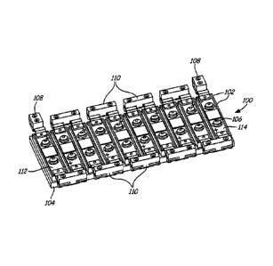
Referring to Figure 1, an LED (assembly) array 100 is shown. The LED
array 100 includes a plurality of LED assemblies 102 attached to a mounting
substrate 104 with a plurality of substrate fasteners such as mounting screws
106. Power is provided to the LED array 100 by means of power connect
5 clamps 108 and the LED assemblies 102 are interconnected using
interconnect clamps 110. One of the end or terminal LED assemblies 112,
114 are disposed at each end of the LED array 100.
Figures 2 and 3 show one embodiment of an LED assembly 102. One
suitable LED assembly is available from Luminus Devices, Inc., 1100
Technology Park Drive, Billerica, MA 01821 USA, as part number SCBT-120-
UV-C14-1382-22. This LED assembly emits electromagnetic radiation
primarily in the UV spectrum, with a peak wavelength of 385 nm. The LED
assembly 102 has positive and negative electrodes 120, 122, and an LED
(chip) 124 in electrical communication with the positive and negative
electrodes 120, 122, at least partially by means of an electrical connector
(wire) assembly 126. In the embodiment depicted in Figure 3 the LED 124 is
covered by a lens 128. The lens 128 may transmit essentially all radiation
emitted from the LED 124 or optionally may filter out selected wave lengths.
Apertures 130, 132 are defined in the base 134. In the embodiment shown
the positive and negative electrodes extend from opposite longitudinal ends of
the base 134. Mounting apertures 136, 138 are defined in respective positive
and negative electrodes 120, 122. Other components and features of the LED
assembly 102 are known to persons of ordinary skill in the art and are not
described herein.
Figure 4 shows an LED assembly 144, the LED assembly differing
CA 02848760 2014-03-13
WO 2013/040453 PC1 /US2012/055568
6
from the LED assembly 102 by the presence of respective positive and
negative electrodes 146, 148. The electrodes 146 148 differ from the
electrodes 120, 122 in that the electrodes 146, 148 are truncated and lack the
apertures 136, 138.
Figures 5 and 6 show bottom and top surfaces of the mounting
substrate 104, respectively. The mounting substrate 104 defines a plurality of
mounting apertures 160, 162 and LED affixing apertures 164, 166. In the
embodiment depicted, the apertures 160, 160 are countersunk, so that
connectors, such as nuts can be used to flush-attach the mounting substrate
104 to a surface, such as present in a printing press. The countersink feature
allows the affixed nuts to be flush with or be entirely below the top surface
168
and, thereby, permit LED assemblies to be mounted flat against the mounting
substrate 104. Thus, the countersink feature permits LED assemblies to fully
contact the top surface 168 when attached thereto. The mounting substrate
104 may be formed from a conductive material, such as copper, aluminum, or
the like.
As shown in Figure 7, one embodiment of a power connect clamp 108
has respective upper and lower portions 172, 174. A power connect clamp
slot 176 is defined between the upper and lower portions 172. 174. In the
embodiment shown, the lower portion 174 is tapered to a maximum
dimension adjacent the slot 176. A power connect clamp aperture 178 is
defined laterally adjacent the slot 176. Threaded power connect clamp
apertures 180, 182 are also formed in the upper portion 172. The threaded
apertures 160, 182 accommodate power connect fasteners such as power
connect set screws 184, 186 or equivalent connectors. In the embodiment
CA 02848760 2014-03-13
WO 2013/040453 PCT/US2012/055568
7
depicted, the aperture 180 opens into the aperture 178. As in the case of the
mounting substrate 104, the clamp 108 may be formed from an electrically
conductive material, such as copper, aluminum, or the like.
As depicted in Figure 8, one embodiment of the interconnect clamp
110 defines respective upper and lower portions 190, 192. Interconnect
clamp slots 194, 196 are formed between the upper and lower portions 190,
192. Threaded interconnect clamp apertures 198, 200 are formed in the upper
portion 190 and open into the respective slots 194, 196. Apertures 202, 204
are formed in the lower portion 192 and are aligned with the respective
apertures 198, 200 in the embodiment depicted. The apertures 198, 200
accommodate interconnect clamp fasteners such interconnect clamp set
screws 206, 208, or equivalent connectors. As in the case with respect to the
mounting substrate 104 and power connect clamp 108, the interconnect
clamp 110 may be formed from electrically connective material, such as
copper, aluminum, or the like.
The LED array 100 is assembled by attaching a plurality of LED
assemblies 102 to the mounting substrate 104 by extending mounting screws
106 through apertures 130, 132, then threading the screws 106 into the
mounting apertures 164, 166. As shown in Figure 1, adjacent LED
assemblies 102 are disposed in alternating polarity such that the positive
electrode of one LED assembly 102 is next to a negative electrode of an
adjacent LED assembly 102. In one embodiment, the electrically insulative
fasteners, e.g., screws 106, are fashioned from an electrically insulative
material to maintain electrical isolation between the base of the LED assembly
and the mounting substrate. One suitable insulative material is Ultern, a
CA 02848760 2014-03-13
WO 2013/040453 PCT/US2012/055568
8
registered trademark for an amorphous thermoplastic polyetherimide (PEI)
resin available from SABIC Innovative Plastics IP B.V. besloten vennootschap
(b.v.) Netherlands Plasticslean 1 Bergen op Zoom Netherlands 4612PX.
Other suitable synthetic resins may be found by a person of ordinary skill in
the art, for example, in the Handbook of Plastics, Elastomers, and
Composites, Charles A. Harper, Editor in Chief, Third Edition, McGraw-Hill,
New York, 1996, hereby incorporated by reference.
The plurality of LED assemblies 102 are interconnected in series by
attaching adjacent positive and negative electrodes pairs to an interconnect
clamp 110. Referring to Figure 6, a positive electrode 120 is disposed within
one of slots 194, 196 and a negative electrode 122 of an adjacent LED
assembly 102 is disposed in the other of the slots 194, 196. The positive and
negative electrodes are then secured in the slots 194, 196 by threading the
screws 206, 208 until they are securely in contact with the electrodes.
Alternatively, high compression spring-loaded contacts may be utilized in lieu
of the threaded fasteners, each providing a gas-tight electrical connection.
The LED assembly 144 may be utilized in lieu of the LED assembly 102, for
example, if saving space is a consideration.
Referring now to Figure 7, LED assemblies 102 at each end of the LED
assembly 100, designated terminal LED assemblies 112, 114, are connected
to an electrical power source, for example by securing a wire or other
conductor positioned in an aperture 178 of the clamp 108 by means of
tightening the set screw 184 within the threaded aperture 180 and tightening
the set screw 166 in the aperture 182.
One of the LED assemblies 102 may be replaced for repair or to alter
CA 02848760 2014-03-13
WO 2013/040453 PCT/US2012/055568
9
the wavelengths being emitted from the LED array 100. The LED assembly is
removed by disconnecting the positive and negative electrodes from the
interconnect clamps or from the interconnect clamp and power connect
clamp, if the item being replaced is a terminal LED assembly. The LED
assembly replacing the removed LED assembly is then attached to the
interconnect clamps or to the interconnect clamp and power connect clamp as
the case may be. The newly attached LED assembly is then attached to the
mounting substrate by the extending the mounting screws through the
apertures 130, 132 and threading them into the apertures 164, 166.
A person of ordinary skill in the art will recognize that both wire and
spade-type electrical conductors can be connectively utilized by the assembly
and method of this invention. Additionally, various densities of physical
mounting may be attained by varying the dimensions and spacing of the LED
assemblies. The various components described herein, and equivalents
thereof, may withstand the high thermal and light energy environment
produced when the LED assemblies are illuminated.
An alternative polarity mounting scheme is utilized to provide series
connection of the LED devices, which is a highly efficient, space-saving
assembly and interconnection method. If necessary, an individual LED
assembly can be removed and exchanged with another individual LED
assembly by loosening one or both of the brackets 108, 110 and removing the
screws 106. The LED assembly intended to replace the removed LED
assembly is then secured within one or both of the clamps 108, 110 and to the
substrate 104 utilizing the set screws 106. This allows replacement of
malfunctioning LED assemblies as well as on-site maintenance and alteration
CA 02 848760 2014-03-13
WO 20131040453 PCT/US2012/055568
of wavelengths produced by the present LED array.
The present assembly and interconnection method of this invention
provides "daisy chaining" in an alternate polarity series circuit by mounting
the
LED assemblies in an alternative polarity.
5 Due to the surface area of the LED assemblies of this invention and
direct contact with a surface area of the mounting substrate, additional
thermal transfer away from the LED heat source is provided.
Because numerous modifications of this invention may be made
without departing from the spirit thereof, the scope of the invention is not
to be
10 limited to the embodiments illustrated and described. Rather, the scope
of the
invention is to be determined by the appended claims and their equivalents.