Note: Descriptions are shown in the official language in which they were submitted.
CA 02882321 2015-02-18
WO 2013/088173 PCT/GB2012/053151
1
Data Transfer
This application relates to methods and apparatus for data transfer,
especially to the
transfer of multiple channels of digital audio data, and in particular to
audio data
transfer that can use a single communications channel.
In many electronic devices there is a need to transmit audio data signals, or
other data
signals, within the electronic devices, or to some peripheral or accessory
device(s) that
may be attached to the electronic devices, for instance a set of headphones.
In many
modern electronic devices, especially devices with RF transmission capability
such as
a mobile telephone or tablet computing device, analogue audio signals are
liable to be
corrupted by electromagnetic interference (EMI) and coupling from other nearby
circuitry. It is therefore desirable to transmit signals from an audio
processing device,
e.g. an integrated circuit audio hub/codec, to the driver of a transducer e.g.
speaker, in
a digital format so as to preserve the integrity and quality of the audio
signal. For audio
data there is also typically a requirement to send data for multiple channels,
for
instance left (L) and right (R) data channels for stereo audio.
Modern electronic devices such as smartphones, tablets and the like typically
transmit
digital audio data using three data wires plus a ground wire. The signal data
for both
L/R audio channels is typically sent on one wire in serial format, for example
in words
of 24 bits, with separate words being sent for the left (L) data channel and
the right (R)
data channel. The bit clock signal (BCLK) is sent on another wire and a
further clock at
the left/right words rate (LRCLK) sent on a further wire as illustrated in
figure 1.
Alternatively, the audio data may be transmitted as a high-rate 1-bit stream,
sometimes
referred to as Pulse Density Modulation (PDM). Word-length reduction, noise
shaping
and/or delta-sigma techniques may be applied to reduce quantisation noise in
the
audio band at the expense of noise at higher frequencies so as to reduce the
required
bit rate. However, this still requires two wires for the transfer of digital
audio data, one
wire for the data and one wire for the clock. Moreover, the digital data
spectrum will
include components corresponding to the base band audio signals, which may
couple
onto other analogue lines associated with the device. Stereo data may be
transmitted
along one wire, typically alternating between sending left channel data and
right
CA 02882321 2015-02-18
WO 2013/088173
PCT/GB2012/053151
2
channel data, but the separate clock line is still needed and the digital data
spectrum
may still present similar problems.
It is therefore an object of the present invention to provide methods and
apparatus for
data transfer of multiple data channels that at least mitigate some of the
aforementioned disadvantages.
Thus according to the present invention there is provided digital data
transmission
circuitry comprising:
at least two data inputs for receiving respective input digital data streams
of data
bits; and
a pulse generator, responsive to said input digital data streams and to a
first
clock signal, to generate a single data pulse having a rising edge and a
falling edge
within each of a plurality of transfer periods defined by said first clock
signal,
wherein the time of occurrence of the rising edge and the falling edge of the
data
pulse encodes the then current data bits of said input digital data streams.
The occurrence said rising and falling edges of the data pulse are quantised
in time
within the transfer period. In this way each data pulse corresponds to one of
a set of
possible data symbols and the data is reversibly encoded, i.e. it may be
recovered by a
suitable decoder. The rising and falling edges of each data pulse may
advantageously
be synchronised to a second clock signal, where the second clock signal has a
frequency greater than the first clock signal. The second clock signal
frequency may
be a multiple of the first clock signal frequency.
The input digital data streams may comprise at least two audio data streams
and/or at
least one stream of control data. The control data may be data for controlling
the
operation of a receiver of the least one audio data stream.
The first clock frequency may be equal to the sample rate of the at least one
digital
data stream. The input data may be oversample data and the sample rate of the
at
least one digital data stream is a multiple of a standard audio frequency
sample rate,
such as 48kHz or 44.1KHz.
CA 02882321 2015-02-18
WO 2013/088173
PCT/GB2012/053151
3
The pulse generator may be configured such that there is at least one period
defined
by the second clock signal at the start of the transfer period before the
start of a data
pulse and/or at least one period defined by the second clock signal at the end
of a data
pulse before the end of the transfer period.
At least one input data stream encoded by the data pulses may comprise a bi-
phase
encoded data stream, for example a Manchester differential encoding data
stream.
The transmission circuitry may therefore comprise a bi-phase encoder for
receiving a
first input data stream and producing the bi-phase encoded input data stream.
The bi-
phase encoder may be configured to generate a bi-phase encoded data stream
comprising at least one illegal bit sequence that is not used for encoding
data. The
illegal bit sequence may be inserted into the bi-phase encoded data stream to
define a
frame of data. The illegal bit sequence may comprise three instances of the
same
value in the bi-phase encoded input data stream and in some embodiments the bi-
phase encoder may generate two instance of the same data value into the bi-
phase
encoded data stream at the start of a frame with the data value matching the
last data
value of the previous frame.
The digital data transmission circuitry may additionally comprise a logic unit
for
performing a logical XOR operation between the current value of an input audio
data
stream and the current value of the bi-phase encoded data stream and the pulse
modulator is responsive to the bi-phase encoded data stream and the output of
the
logic unit.
In some embodiments at least some data pulses having the same duration encode
different data values.
The pulse generator may be configured such that the rising or falling edge at
the start
of the data pulse occurs substantially no later than half way through the
transfer period
and/or the rising or falling edge at the end of the data pulse occurs
substantially no
earlier than half way through the transfer period.
CA 02882321 2015-02-18
WO 2013/088173 PCT/GB2012/053151
4
The pulse generator may configured such that the set of possible data pulses
that may
be transmitted comprises at least one data pulse which has a duration which is
unique
within the set. The set of possible data pulses may comprise a minimum
duration data
pulse which has a duration which is unique within the set and which is shorter
than the
duration of any other data pulse within the set. The circuitry may be operable
in a
synchronisation phase to transmit a sequence of data pulses comprising at
least one
data pulse which has a duration which is unique within the set.
The pulse generator may be configured such that at least one possible
combination of
input data can be encoded by more than one possible data pulses. Overtime,
different
instances of said combination of input data may be encoded by different ones
of said
possible data pulses. The different possible data pulses for encoding a given
combination of input data may have different durations and the pulse may
select
between the possible data pulses so as to minimise any d.c. imbalance over
time in the
transmitted data pulses. One of the possible data pulses for encoding a given
combination of input data may have a duration of greater than half the
transfer period
and another of the possible pulses may have a duration of less than half the
transfer
period.
The pulse generator may be configured such that there is at least one possible
data
pulse that is not used to encode the input data but which may be transmitted
by the
pulse generator for synchronisation and/or control.
At least one of the data inputs may be configured to receive an input digital
data stream
which is a n-bit data stream. In some embodiments n=1. At least one input
digital data
stream may be a PDM data stream and/or at least one of said data inputs may be
configured to receive an input digital data stream which is a PCM data stream.
The digital data transmission circuitry as claimed may comprise a combination
module
for receiving at least first and second data streams and producing a combined
data
stream as one of said input digital data streams, wherein said combined data
stream
comprises one or more bits of the first audio data interleaved with one or
more bits of
the second data stream.
CA 02882321 2015-02-18
WO 2013/088173
PCT/GB2012/053151
The digital data transmission circuitry may have a first data output terminal
associated
with transmission of said data pulses to a receiver and said first output
terminal is the
only output terminal associated with said data transfer. Alternatively there
may be a
first data output terminal associated with transmission of said data pulses to
a receiver
5 and a second output terminal for transmitting a clock signal for defining
the transfer
period.
The output from the pulse generator may be connected to an audio signal path
on a
printed circuit board of a host device and/or a connector of a host device,
which may
for example be a socket. The connector may comprise a connection for an audio
accessory. In some embodiments the circuitry is configured, in use, to provide
audio
data and power to a peripheral connected to said connector. The connector may
have
connections for audio data-out, power and ground. In some instances the power
connection also serves as said audio data-out connection. There may
additionally be
an audio data-in connection. The audio data-in connection may also serves as
the
audio data-out connection. The connector may be an optical connector.
The digital data transmission circuitry may comprise bi-directional interface
circuitry
configured to transmit said data pulses generated by the pulse generator over
a first
communications link and receive data pulses via said first communications
link. The
pulse generator may be configured to transmit data pulses during a first
transfer period
and the bi-directional interface circuitry is configured to receive data pulse
during a
second, different transfer period. The bi-directional interface circuitry may
comprise a
drive circuit for voltage modulating the first communications link based on
the data
pulses and a read circuit responsive to the resultant voltage on the first
communications link, wherein the read circuit is configured to subtract the
drive voltage
modulation from the resultant voltage signal.
Embodiments of the invention also relate to a digital receiver. Thus in
another aspect
of the invention there is provided digital data receiver circuitry comprising:
an input for receiving a series of data pulses,
a sampler for sampling each received pulse within a transfer period defined by
a
first clock signal such that there is a single data pulse with a rising edge
and a falling
edge in each transfer period, said sampler being configured to provide an
indication of
CA 02882321 2015-02-18
WO 2013/088173 PCT/GB2012/053151
6
which of a set of possible data symbols the data pulse corresponds to based on
the
timing of the occurrence of both the rising and falling edges of the data
pulse within the
transfer period; and
decoding circuitry for generating at least one received digital data stream
based
on said indication,
wherein said decoding circuitry is configured such that a plurality of
possible data
symbols may be decoded as the same value of a data bit of a received digital
data
stream.
The decoding circuitry may generate at least two received digital data streams
based
on said indication.
The digital data receiver circuitry may comprise a clock recovery circuit for
recovering a
clock signal from said series of data pulses and generating said first clock
signal. The
clock recovery circuit may generate a second clock signal at a frequency which
is a
predefined multiple of the frequency of the first clock signal. The second
clock signal
may be generated so as to be synchronised to the timing of the rising and
falling edges
of the data pulses within the transfer period.
The set of possible data symbols that may be received may comprise at least
one data
symbol which has a pulse duration which is unique within the set. In which
case the
digital data receiver circuitry may be configured to identify receipt of said
at least one
data symbol which has a pulse duration which is unique within the set and use
receipt
of such a data symbol to synchronise the start and end of the transfer period.
The
receiver circuitry may be operable in a synchronisation phase to receive a
sequence of
data pulses comprising at least one data symbol which has a pulse duration
which is
unique within the set and to derive said first and second clock signals, with
said first
clock signal being synchronised to the transfer period.
In some embodiments however the digital data receiver may have a clock input
for
receiving a first clock signal defining the transfer period. In which case
there may be
circuitry for generating a second clock signal from said received first clock
signal, the
frequency of the second clock signal being a predefined multiple of the
frequency of the
CA 02882321 2015-02-18
WO 2013/088173
PCT/GB2012/053151
7
first clock signal, wherein the second clock signal is generated synchronised
to the
timing of the rising and falling edges of the data pulses within the transfer
period.
The received digital data streams may comprise at least two audio data streams
and/or
at least one stream of control data. The control data may be data for
controlling the
operation of an audio component which comprises said digital data receiver
circuitry.
At least one received data stream encoded by said data symbols may be a bi-
phase
encoded data stream, for example a Manchester differential encoded data
stream. A
bi-phase decoder may decode said bi-phase encoded data stream. The bi-phase
decoder may be configured to identify at least one illegal bit sequence that
is not used
for encoding data. The illegal bit sequence may be identified to define a
frame of data.
The illegal bit sequence may comprise three instances of the same value in the
bi-
phase encoded data stream. On detection of three instances of the same value
in the
bi-phase encoded data stream, the data pulses encoding the second and third
instances may be identified as the first two data pulses of a new frame.
The receiver circuitry may also comprise a logic unit for performing a logical
de-XOR
operation between the current value of a first received digital data stream
and the
current value of the bi-phase encoded data stream and the output of the logic
unit is
used as the output data for the first digital data stream.
The data recovery circuit may output at least one received digital data stream
which is
a 1-bit PDM data stream and/or at least one received digital data stream which
is a
PCM data stream.
The receiver circuitry may have a separation module having an input for a
received
data stream and configured to produce at least first and second data streams,
wherein
said first and second data streams are recovered by taking one or more bits
from the
received data stream that correspond to the first data stream and which are
interleaved
with one or more bits of the second data stream.
In some embodiments there may be at least a first data extraction module and a
second data extraction module wherein the first data extraction module and the
second
CA 02882321 2015-02-18
WO 2013/088173 PCT/GB2012/053151
8
data extractions module are configured to determine data values for different
received
data streams to one another. The first data extraction module may be
configured to
receive the input data pulses from the interface and to pass said data pulses
to the
second data extraction module. Each of the at least first and second data
extraction
modules may be associated with respective first and second audio transducers.
In some embodiments the circuitry may comprise power circuitry configured to
derive a
power supply from said input serial pulse-length modulated audio data signal.
The
sampler and decoder circuitry may be powered by said power supply.
The digital data receiver circuitry may be implemented in an accessory device
such as
a headset.
The invention also relates to a digital data transceiver circuitry comprising
digital data
transmission circuitry as described above to send digital data and digital
data receiver
circuitry as described above to receive digital data.
In a further aspect of the invention there is provided a digital interface
comprising:
a data encoder for receiving at least two streams of digital data to be
transmitted
and a first clock signal, and generating a series of data pulses at a digital
data output,
said series of pulses being encoded according to a first digital data protocol
such that
there is a single data pulse having a rising and falling edge in each of a
plurality of
transfer periods defined by said first clock signal, the at least two streams
of digital data
to be transmitted being encoded by the timing of the occurrence of the rising
and falling
edges of the data pulse within the transfer period; and
a data decoder for receiving a series of encoded data pulses at a digital data
input and decoding at least one received data stream, said encoded data pulses
being
encoded using said first digital data protocol at a data input.
The digital interface may be configured as a master circuit for controlling a
digital data
bus from said master to at least one slave component. In which case the data
encoder
may be configured to transmit data to a plurality of slave components
connected in a
chain configuration and said data decoder is configured to received data from
the last
slave component in the chain. The interface may be configured to transmit
audio data
CA 02882321 2015-02-18
WO 2013/088173 PCT/GB2012/053151
9
for at least one slave component having an audio output transducer and control
data
for controlling at least one slave component. The control data may be
transmitted in
frames.
Alternatively the digital interface may be configured as a slave circuit on a
digital data
bus.
In some embodiments the digital decoder may be configured to receive data
pulses at
said digital data input from an upstream audio circuit, decode said data
pulses, identify
any audio data and/or control data for said audio component, and the digital
encoder
may be configured to generate data pulses for a downstream audio component
based
on said decoded data and any required modifications of the control data. The
component having the interface may comprise at least one source of audio data
and
the data pulses generated for the downstream component may encode audio data
from
said source of audio data.
The invention also relates to a system comprising at least first and second
components
having a signal path between them such that data to be transmitted to or
received from
the second component is transmitted via the first component, wherein the first
component comprises a digital interface as described above. The first
component may
be configured to receive a series of said data pulses encoding data for at
least one
component and to forward a signal to said second component. The series of data
pulses may encode data for said first component and the first component may be
configured to extract said data for said first component. The first component
may also
forward the series of data pulses received to the second component. The first
component may decode the data in the series of data pulses received and use at
least
some of said decoded data to generate a series of data pulses for transmission
to the
second component. The first component may generate the series of data pulses
for
transmission to the second component to encode data generated by said first
component. The system may comprise a plurality of audio components with each
component being connected to the next component in a chain.
Any of the circuits discussed above may be implemented as an integrated
circuit and/or
may be embodied in an electronic device, which may be at least one of: a
portable
CA 02882321 2015-02-18
WO 2013/088173
PCT/GB2012/053151
device; a battery powered device; a communication device; a computing device;
a
personal media player; a music player; a mobile telephone; a docking station
for a
portable device; a headset; and a hearing aid.
5 The
invention also relates to methods of data transfer. Thus in another aspect of
the
invention there is provided a method of digital data transfer comprising
defining a
transfer period based on a clock signal, transmitting a single data pulse
within each
transfer period such that each data pulse a distinct rising and falling edge
within the
transfer period and encoding data at least two input digital data streams by
setting
10 times of
occurrence of the rising and falling edges of the data pulse within the
transfer
period.
The method may be performed using any of the implementations discussed above
in
respect to the other aspects of the invention.
Embodiments of the invention allow low latency data transfer which is
particularly
appropriate for transfer of digital data from one audio apparatus to another,
for example
for noise cancellation. In another aspect of the invention there is provided
an audio
apparatus comprising:
at least first and second audio input transducers; and
a connector for connecting said audio apparatus to an electronic device, said
connector having at least three contacts, configured such that:
a first of said contacts provides a supply current for said apparatus;
a second of said contacts is a ground return; and
a third of said contact carries a first digital composite signal comprising
oversampled signals from said at least two audio input transducers
The signals from said at least two audio input transducers may oversampled at
a data
rate of at least 700 kilosamples per second or at least 3 megasamples per
second
The apparatus may comprise a data encoder responsive to said audio input
transducers to generate said first digital composite signal. The data encoder
may
comprise a data transmitter according to the first aspect of the invention.
The data
encoder may be configured to generate said first digital composite signal by
generating
CA 02882321 2015-02-18
WO 2013/088173 PCT/GB2012/053151
11
one data pulse within each of a plurality of transfer periods defined by a
clock signal,
each pulse having a single rising edge and a single falling edge; wherein the
time of
one or both of the rising edge and the falling edge of the data pulse encodes
the
current respective samples of both the said delta-sigma-modulated audio input
data
signals.
The audio input transducers may be microphones. The apparatus may be an audio
accessory apparatus for use with an electronic device, for example the audio
accessory apparatus may be a headset.
The connector may comprise a male-type plug, for example a 3.5mm TRS or TRRS
jack plug.
The at least two audio input transducers may be configured to detect ambient
noise.
The apparatus may comprise at least two loudspeakers for audio playback
wherein
said at least two audio input transducers are configured to detect ambient
noise in the
vicinity of said loudspeakers. The connector may therefore comprise at least a
fourth
contact for receipt of audio data for said loudspeakers. The apparatus may
comprise
receiver circuitry for recovering first and second audio signals from a second
composite
digital audio signal received via said fourth contact, and conversion
circuitry for
applying the first and second audio signals to said speakers. The receiver
circuitry
may be receiver circuitry according to the aspect of the invention discussed
above. In
particular the second digital composite signal may comprise one data pulse
within each
of a plurality of transfer periods, each pulse having a single rising edge and
a single
falling edge, wherein the time of both the rising edge and the falling edge of
the data
pulse encodes the current samples of both the said delta-sigma-modulated
speaker
signals.
Embodiments of the invention also relate to an electronic device comprising a
device
connector for connecting to the apparatus connector of the audio apparatus
according
to this aspect of the invention, the electronic device comprising a decoder
for receiving
said first digital composite signal, to extract separate audio input signals,
to calculate
respective signals to cancel the ambient noise, and to combine these
correction signals
into the second composite digital signal as above for transmission to the
loudspeakers.
CA 02882321 2015-02-18
WO 2013/088173
PCT/GB2012/053151
12
An audio ambient noise cancellation system comprising a device discussed above
connected to an apparatus as discussed above is also provided.
In another aspect of the invention there is provided audio interface circuitry
comprising:
a pulse generator, responsive to at least one digital audio data stream and at
least one control data stream, to generate one data pulse within each of a
plurality of
transfer periods defined by a clock signal,
wherein each data pulse has a single rising edge and a single falling edge and
wherein the timing of at least one of the rising edge and the falling edge of
the data
pulse within the transfer period is based on a combination of the then current
values of
said at least one digital audio data stream and said control data stream.
The invention also provides an audio accessory comprising:
a plurality of wired connections to a connector, said connector comprising:
a first connection for carrying supply current for circuitry in the accessory;
a second connection for carrying ground return current for circuitry in the
accessory; and
a third connection for carrying a first oversampled digital composite signal.
The connector may further comprise a fourth connection for carrying a second
oversampled digital composite signal.
In a yet further aspect the invention provides audio interface circuitry
comprising:
a pulse-length-modulator, responsive to a plurality of data streams of audio
data
samples at a sample rate, to generate a stream of data pulses at said sample
rate;
wherein the length of each said data pulse is dependent upon on a combination
of the then current audio data samples from said plurality of data streams.
The audio data streams may comprise 1-bit digital audio data streams and/or
may
correspond to audio data channels.
The pulse-length-modulator may be responsive to a first clock signal having a
frequency equal to said sample rate. The pulse-length-modulator may also be
further
CA 02882321 2015-02-18
WO 2013/088173
PCT/GB2012/053151
13
responsive to a second clock signal, wherein the second clock signal has a
frequency
which is a multiple of the frequency of the first clock signal and wherein the
length of
each data pulse is based on a selected number of cycles of the second clock
signal.
The minimum data pulse length may be a plurality of cycles of the second clock
signal.
The maximum data pulse length may be shorter than the period of the first
clock signal
by a plurality of cycles of the second clock signal.
The pulse-length-modulator may be configured so that at least one combination
of
input audio data for said plurality of audio data streams can be encoded as at
least two
different alternative data pulse lengths. The pulse-length-modulator may be
configured
so as to vary between said at least two different alternative data pulse
lengths when
encoding said at least one combination of input audio data and may alternate
between
said at least two different alternative data pulse lengths when encoding said
at least
one combination of input audio data. The pulse-length-modulator may randomly
select
one of said at least two different alternative data pulse lengths when
encoding said at
least one combination of input audio data and/or may, when encoding said at
least one
combination of input audio data, vary between said at least two different
alternative
data pulse length so as to control the average data pulse length for all
instances of a
given combination of input audio data. A plurality of combinations of input
audio data
may each be encoded as a plurality of alternative data pulse lengths and the
pulse-
length-modulator may vary between the respective alternative data pulse length
so that
the average data pulse length for each combination of input audio data is
substantially
the same. A plurality of combinations of input data may each be encoded as two
different lengths of data pulse, the two lengths being symmetric about a
predetermined
length. One combination of input data may be encoded as a data pulse having a
length substantially equal to said predetermined length.
The pulse-length-modulator may be configured to receive at least one
additional data
channel and wherein the length of at least some individual data pulses encodes
the
then current audio data samples from said plurality of data streams and also
the then
current data sample for said additional data channel. The additional data
channel may
be a control data channel. When no data is received on said additional data
channel
the pulse length modulator may vary between pulse lengths that encode the same
audio data combination. When data is received on an additional data channel
the
CA 02882321 2015-02-18
WO 2013/088173 PCT/GB2012/053151
14
pulse-length-modulator may modulate a series of data pulses with a first
reserved
sequence prior to encoding said data of the additional data channel, where the
first
reserved sequence corresponds to the encoding that would be used for a
particular
data sequence on the additional data channel and wherein the pulse-length-
modulator
is configured so as not to use the first reserved sequence when no data is
available on
the additional data channel. When data on the additional channel stops a
second
reserved sequence of additional data may be encoded.
The frequency of the second clock signal may be at least five times, or
possibly at least
eight times, the frequency of the first clock signal.
The plurality of audio data streams may comprise left and right stereo data
channels.
The pulse-length-modulator may be configured to receive a separate audio data
stream
for each of said audio channels. The pulse-length-modulator may comprise a
combiner
for producing a combined data value from each of said audio data streams.
A counter may be arranged to count at a frequency of the second clock signal
and a
comparator may be arranged to compare the count value to the combined data
value.
The pulse-length-modulator may be configured to produce an output which varies
between a first non zero voltage and a second non zero voltage.
The rising edges of the data pulses may be separated by a regular time
interval equal
to the sample period. The falling edges of the data pulses may be separated by
a
regular time interval equal to the sample period.
The output from the pulse-length-modulator may be connected to an audio signal
path
on a printed circuit board of a host device and/or to a connector of a host
device, such
as a socket. The connector may comprise a connection for a headset. The pulse-
length-modulator may be configured, in use, to provide audio data and power to
a
peripheral connected to said connector. The connector may comprise connections
for
audio data-out, power and ground. The power connection may also serve as said
audio data-out connection. There may also be an audio data-in connection. In
some
CA 02882321 2015-02-18
WO 2013/088173 PCT/GB2012/053151
embodiments the audio data-in connections also serves as the audio data-out
connection. The connector may be an optical connector or an rf transmitter.
The audio interface circuitry may further comprising bi-directional interface
circuitry
5 configured to transmit said data pulses generated by the pulse-length-
modulator over a
first communications link and receive pulse-length-modulated data pulses via
said first
communications link. The pulse-length-modulator may be configured to transmit
data
pulses during a first portion the sample period and the bi-directional
interface circuitry is
configured to receive data pulse during a second, different portion of the
sample
10 period. The bi-directional interface circuitry may comprise a drive
circuit for voltage
modulating the first communications link based on the data pulses and a read
circuit
responsive to the resultant voltage on the first communications link, wherein
the read
circuit is configured to subtract the drive voltage modulation from the
resultant voltage
signal.
In a further aspect of the invention there is provide an audio circuitry
comprising:
an interface configured to receive a serial pulse-length modulated audio data
input comprising a series of data pulses at a sample rate;
data extraction circuitry configured to determine the pulse length of said
data
pulse and to determine a data value for each of a plurality of audio data
streams from
said pulse length.
The circuitry may comprise clock recovery circuitry configured to recover a
first clock
signal based on said sample rate. The data extraction circuitry may be
configured to
sample the data pulse at a predetermined number of intervals within the period
of the
first clock signal to determine the pulse length of the data pulse. The data
extraction
circuitry may comprise a delay line having a plurality of tap points. The data
extraction
circuitry may comprise at least a first data extraction module and a second
data
extraction module wherein the first data extraction module and the second data
extractions module are configured to determine data values for different audio
data
streams to one another. The first data extraction module may be configured to
receive
the input serial pulse-length modulated audio data from the interface and to
pass said
input serial pulse-length modulated audio data to the second data extraction
module.
Each of the at least first and second data extraction modules may be
associated with
CA 02882321 2015-02-18
WO 2013/088173 PCT/GB2012/053151
16
respective first and second audio transducers. The circuitry may further
comprise
power circuitry configured to derive a power supply from said input serial
pulse-length
modulated audio data signal. The data extraction circuitry may powered by said
power
supply.
The audio circuitry may be implemented in a headset and/or may be arranged as
a
transceiver. An audio system is also provided.
In a further aspect there is provided a method of transmitting audio data
comprising,
generating a pulse length modulated signal comprising a series of data pulses
at a
sample rate;
wherein the length of each data pulse is dependent upon on a combination of
then
current audio data samples from said plurality of data streams.
Aspects of the invention further relate to an audio system for transferring
audio data for
a plurality of audio channels over a single wire connection comprising a pulse-
length-
modulator configured to produce a series of data pulses at regular intervals
wherein the
length of each data pulse encodes audio data for each of said plurality of
audio
channels.
Aspects of the invention further relate to data transfer system for
transferring data for a
plurality of separate data channels over a single wire connection comprising a
pulse-
length-modulator configured to produce a series of data pulses at regular
intervals
wherein the length of each data pulse encodes data from each of said plurality
of audio
channels.
Aspects of the invention further relate to audio interface circuitry
comprising:
a pulse-length-modulator responsive to audio data for a plurality of audio
channels to
generate data pulses at a regular time interval;
wherein the length of the data pulses encode said audio data; and
wherein the length of an individual data pulse encodes audio data for said
plurality of
audio channels.
CA 02882321 2015-02-18
WO 2013/088173
PCT/GB2012/053151
17
Aspects of the invention further relate to an audio interface for receiving
and encoding
a plurality of streams of 1-bit audio data samples and for transmitting a
stream of
encoded data pulses via a single communication link."
Aspects of the invention further relate to an audio interface for receiving
and encoding
a plurality of streams of 1-bit audio data samples and simultaneously
transmitting on a
clock edge of a stream of encoded data pulses a plurality of sampled 1-bit
audio data
samples via a single communication link.
In a yet further aspect of the invention there is provided audio interface
circuitry for
transfer of audio signals wherein said interface circuitry is operable in:
an analogue mode for receiving analogue audio signals; and
a digital mode for receiving digital audio signals
wherein, in said digital mode,
said digital audio signals comprise a series of data pulses wherein the length
of
each pulse encodes at least two audio digital data streams, and
wherein the interface circuitry decodes at least one of said digital data
streams.
The data may alternatively be encoded by the timing of the occurrence of the
rising and
falling edges of the data pulse within a transfer period defined by a first
clock signal.
The interface circuitry may decode and condition at least one of said digital
data
streams.
The interface circuitry may comprise: at least a first analogue signal path
for receiving
analogue audio data from a first contact on a connector; at least a first
digital path for
receiving digital audio signals from the first contact on the connector; and
at least a
first switch for enabling/disabling the first analogue signal path. It may
further
comprise: a second analogue signal path for transferring analogue audio data
to/from a
second contact on a connector; a second digital path; a second switch for
enabling/disabling the second analogue signal path. The at least first and
second
switches may default to enabling the first and second analogue signal paths
and may
comprise depletion modes FETs within the first and second analogue signal
paths
respectively. The second analogue path may be for receiving an audio signal
from said
CA 02882321 2015-02-18
WO 2013/088173 PCT/GB2012/053151
18
contact and said second digital path may be for transferring digital audio
signals to said
second contact. There may also be a third analogue signal path for
transferring
analogue audio data to/from a third contact on a connector; a third digital
path, wherein
said third digital path is a path providing power to the interface circuitry
from a third
contact of a connector; and a third switch for enabling/disabling the third
analogue
path. The third switch may default to enabling the third analogue signal path.
The third
analogue signal may be for transferring analogue audio data to the third
contact of the
connector.
The interface circuitry may comprise circuitry configured to, in the digital
mode, derive
power from digital audio signals received on said first digital data path.
The first and second analogue signal paths may be for receiving audio data for
respective loudspeakers. The third analogue signal path may be for
transferring audio
data to the connector from a microphone. Digital decoding circuitry may be
coupled to
said first digital path configured to decode said data pulses in the digital
mode. Digital
encoding circuitry may be coupled to said second digital path configured to
encode
data pulses in the digital mode. Discrimination circuitry may be configured
to, when
power is available on the third digital path, to determine whether to operate
in the
digital mode and, if so, generate a control signal to disable the analogue
signal paths.
The discrimination circuitry may be configured to, when power is available on
the third
digital path, to attempt handshaking with a device connected via said
connector.
There may be a ground path for connecting to a ground contact on a connector
in both
said digital and said analogue mode.
The audio interface circuitry may be implemented as an integrated circuit. An
audio
apparatus may include such audio interface circuitry and at least a first
audio output
transducer, where said interface circuitry is configure to forward a received
analogue
audio signal to said first audio output transducer in the analogue mode and to
decode
said digital audio signal and forward a decoded digital data stream to said
first audio
output transducer in the digital mode.
CA 02882321 2015-02-18
WO 2013/088173
PCT/GB2012/053151
19
The audio apparatus may comprise at least first and second audio output
transducers
wherein, when enabled, said first and second analogue signal paths provides a
direct
connection to said first and second audio output transducers respectively.
Digital
decoding circuitry may comprise first and second analogue outputs for
connecting to
said first and second audio output transducers respectively. The first and
second
switches may switch between the first and second analogue signal paths and the
first
and second outputs of the digital decoding circuitry. The first and second
signal paths
may be connected to first and second converters for converting between
analogue and
digital signals such that any analogue audio signals received for the
transducers are
converted to corresponding digital signals. Digital processing circuitry may
be
configured to apply digital processing to the digital signals output from said
first and
second converters. The digital processing circuitry may comprise analogue
outputs for
connecting to said first and second transducers respectively.
The interface circuitry may be connected to a connector and said connector is
a TRRS
jack. The apparatus may be an accessory apparatus configured to be connected
to an
electronic device, such as an audio headset.
Aspects of the invention also provide a method of receiving audio signals
comprising:
receiving said audio signals at an interface operable in analogue mode and
also in
digital mode and selecting a mode to operate in, wherein:
in said analogue mode at least one analogue audio signal is received and
forwarded
for an audio output transducer; and
in said digital mode at least one digital audio signal is received, said
digital audio signal
comprising a series of data pulses wherein the length of each pulse encodes at
least
two audio data streams, and the interface circuitry decodes at least one of
said data
streams and forwards said digital data stream for an audio output transducer.
The method may comprising determining whether a connected device transmitting
the
audio signals is capable of sending signals suitable for the digital mode and,
if so
operating in the digital mode, otherwise operating in the analogue mode.
Aspects of the invention also provide interface circuitry for receiving audio
signals
wherein said interface circuitry is operable:
CA 02882321 2015-02-18
WO 2013/088173
PCT/GB2012/053151
in an analogue mode to receive analogue audio signals; and
in a digital mode to receive digital audio signals wherein, in said digital
mode, the audio
data comprises a series of data pulses at a pulse rate wherein the length of
each pulse
encodes at least two audio data streams.
5
In a further aspect there is provided interface circuitry for transmitting
audio signals to
an apparatus external to a host device wherein said interface circuitry is
operable:
in an analogue mode to transmit analogue audio signals; and
in a digital mode to transmit digital audio signals wherein, in said digital
mode, the
10 audio data comprises a series of data pulses at a pulse rate wherein the
length of each
pulse encodes at least two audio data streams.
In a further aspect there is provided audio interface circuitry comprising:
at least first and second analogue signal paths for transmitting analogue
audio data to
15 respective first and second contacts on a connector;
at least a first digital path for transmitting digital audio signals to the
first contact on the
connector; and
at least a second digital path coupled to a second contact on the connector.
20 The second digital path may be for receiving digital data from the
second contact in
digital mode. A third analogue signal path may be provided for receiving
analogue
audio data from a third contact on a connector; with a third digital path for
transmitting
power to the third contact on the connector in digital mode. A first interface
may be
provided for digital communication with a first component of a host device and
a
second interface for digital communication with a second component of a host
device.
There may be a digital only path for communication between said first and
second
interfaces. The first component may comprise an applications processor, a
baseband
processor, a transmission codec or a wireless codec.
The invention also provides, in a further aspect, a headset for receiving
audio signals
comprising at least one audio output transducer and a connector for connecting
to an
audio device wherein the headset is operable in
a digital mode for receiving digital audio signals via said connector and
applying said
digital audio signals to said at least one audio output transducer and
CA 02882321 2015-02-18
WO 2013/088173 PCT/GB2012/053151
21
an analogue mode for receiving analogue audio signals via said connector and
applying said received analogue audio signals said at least one audio output
transducer.
In a yet further aspect there is provided an audio apparatus comprising:
at least first and second audio output transducers;
a connector for connecting the audio apparatus to another device having at
least first
and second contacts;
interface circuitry operable:
in a first mode to enable first and second analogue signal paths from the
first and
second contacts directly to the first and second audio output transducers
respectively;
and
in a second mode to disable said first and second analogue signal paths and
provide at
least a first digital signal path from the first contact to a digital decoder.
In said digital mode the interface circuitry provides power to the digital
decoder from
the second contact.
CA 02882321 2015-02-18
WO 2013/088173
PCT/GB2012/053151
22
The invention will now be described by way of example only with reference to
the
following drawings, of which:
Figure 1 illustrates a prior art three-wire data transfer protocol for stereo
audio data;
Figure 2 illustrates a data transfer system according to an embodiment of the
present
invention and figure 2b illustrates another embodiment of a data transfer
system;
Figure 3 illustrates examples of symbols that may be transmitted;
Figure 4 illustrates one embodiment of suitable transmitter circuitry;
Figure 5 illustrates the data waveforms on various signals lines of the
embodiment
shown in Figure 4;
Figure 6 illustrates one embodiment of suitable receiver circuitry;
Figure 7 illustrates an alternative arrangement for providing synchronisation
in the
receiver circuitry shown in Figure 6;
Figure 8 illustrates a set of symbols used in one embodiment;
Figures 9a and 9b illustrate embodiments of the invention arranged as a chain
of audio
components;
Figures 10a and 10b show examples of slave device configurations;
Figure 11 illustrates example data waveforms on the various signal lines of
the
embodiment illustrated in Figure 2b when using a fixed rising edge;
Figure 12 illustrates one embodiment of a suitable audio transmitter for the
embodiment shown in figure 11
CA 02882321 2015-02-18
WO 2013/088173
PCT/GB2012/053151
23
Figure 13 illustrates example waveforms on the various signal lines of the
transmitter
embodiment illustrated in Figure 12;
Figure 14 illustrates one embodiment of a suitable audio data receiver for the
embodiment shown in figure 11;
Figure 15 illustrates example waveforms on the various signal lines of the
receiver
embodiment illustrated in Figure 14;
Figure 16 illustrates one example of an encoding scheme which allows data
input
combinations to have alternative possible encodings;
Figure 17 illustrates a data transfer system according to another embodiment
of the
present invention using a fixed rising or falling edge;
Figure 18 illustrates another example of an encoding scheme;
Figure 19 illustrates an embodiment of interface circuitry for sending PLM
data in both
directions over a single data link;
Figure 20 illustrates examples waveforms on the various signal lines
illustrated in
Figure 19;
Figure 21 illustrates another embodiment of interface circuitry for sending
PLM data in
both directions over a single data link;
Figure 22 illustrates an application of an embodiment of the invention;
Figure 23 illustrates an application of another embodiment of the invention;
Figure 24 illustrates an application of a further embodiment of the invention;
Figure 25 illustrates an application of another embodiment of the invention;
CA 02882321 2015-02-18
WO 2013/088173
PCT/GB2012/053151
24
Figure 26 illustrates an application of a yet further embodiment of the
invention;
Figure 27 illustrates an application of a further embodiment of the invention;
Figure 28 illustrates an application of another embodiment of the invention;
Figure 29 illustrates various consumers and generators of data in a device and
a
connected accessory apparatus;
Figure 30 illustrates a first embodiment of the invention for transferring
data in the
arrangement shown in Figure 29;
Figure 31 illustrates a second embodiment of the invention for transferring
data in the
arrangement shown in Figure 29;
Figure 32 illustrates a connection interface for an accessory according to an
embodiment of the invention;
Figure 33 illustrates a connection interface for an accessory according to
another
embodiment of the invention; and
Figure 34 illustrates a connection interface for a device according to an
embodiment of
the invention;
Figure 35 illustrates an electronic device with various connections for
accessory
apparatuses; and
Figure 36 illustrates various connections between internal and external
systems of an
electronic device.
As mentioned above increasingly audio data is being stored and transmitted in
digital
form. For instance in a portable device such as a mobile telephone or tablet
computing
CA 02882321 2015-02-18
WO 2013/088173 PCT/GB2012/053151
device, there may be an audio digital signal processor or audio codec which
processes
the audio data and which transmits audio data to and from audio transducers
such
loudspeakers and/or microphones which may be provided on the host device
and/or
which may be connected to the host device via a suitable interface. There are
5 advantages in transmitting such data to and from the transducers in a
digital format but
conventional digital transfer often requires multiple signal paths, e.g. for a
data signal, a
bit clock and a frame clock as described previously with reference to Figure
1.
Providing multiple wires, or conductive tracks, routed around the device all
carrying
various signals can be disadvantageous in terms of cost, electromagnetic
interference
10 and power consumption. There is therefore a desire to transmit data,
especially audio
data, between components using minimal wires carrying maximal data. There is
also a
desire for low latency data transfer, especially in applications such as
ambient noise
cancellation.
15 Embodiments of the present invention relate to data protocols, data
interfaces and
methods and apparatus for data transfer that allow high speed/low latency and
accurate digital data transfer of multiple channels of data that can be
implemented with
very few wires/links ¨ and in many cases a single link. The embodiments have a
simple physical interface with fewer connections than many other known data
20 interfaces operating other data protocols. The embodiments are suitable
for point-to-
point connection of audio producing and consuming components and also
connecting
several components of a device, thus providing a high speed audio data bus
without
requiring several parallel links. Embodiments also relate to connection of
peripheral
devices, often referred to as "accessories", such as headsets or the like
which can use
25 digital data transfer and which may also be compatible with legacy
systems and
connection components. The low latency of the data transfer is very suitable
for
applications such as ambient noise cancellation.
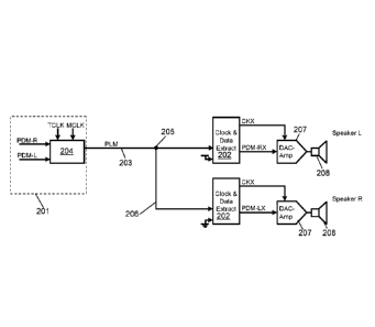
Figure 2 illustrates one embodiment of a data transfer system for transferring
digital
data over a link 203, i.e. conductive path, between a first component 201 and
a second
component 202. The apparatus is suitable for transferring multiple
simultaneous
channels of data over a single link. In this example stereo audio data is
transferred,
optionally along with control data for controlling the set-up and operation of
transducers
such as microphones and speakers for example. The first component 201 may be
CA 02882321 2015-02-18
WO 2013/088173 PCT/GB2012/053151
26
audio interface circuitry that is incorporated as part of an audio codec or a
digital signal
processor of a host device for example. The second component 202 may be audio
interface circuitry, for example as part of transducer driving circuitry. The
second
component 202 may be part of the same host device as the first component 201
and
thus the link 203 may comprise a trace on a PCB of the host device or other
permanent
wired connection. Alternatively the second component 202 could be part of a
separate
device to the first component 201. For example the first component 201 could
be
located in a media player or mobile telephone or the like and the second
component
202 could be part of a second device, for example a peripheral or accessory
device,
that is coupled in use such as a headset or docking station or the like. In
this case the
link 203 may comprise a conductive path involving a suitable connection (not
shown)
such as a plug and socket. In further embodiments the first and second
components
may both be implemented on the same integrated circuit, and the link is an on-
chip
connection, to reduce the width of interconnect bussing between circuit
blocks.
Various applications of the embodiments of the present invention will be
described in
more detail later.
The audio interface circuitry of the first component 201 comprises a modulator
which
receives audio data input data, PDM-R and PDM-L, for the left (L) and right
(R) audio
channels. In this example the LJR input data are separate 1-bit, i.e. Pulse
Density
Modulation (PDM) digital input data streams for each channel, i.e. left
channel and right
channel. In some applications the modulator may also receive control data CTRL
to be
transmitted to the second component for controlling transducers for example.
The modulator implements a protocol to transmit data that ensures that data,
possibly
multiple channels of data, and a clock are encoded into a single pulse stream.
ENCODING
The encoding protocol operates by transmitting data in the form of data pulses
in data
transfer periods defined by a data transfer clock signal. The data pulses
reversibly
encode the data payload to be transmitted ¨ in other words the original data
payload
can be decoded unambiguously from the data pulse. The transfer period is
defined by
a data transfer clock signal which may be derived from a supplied clock
signal, for
CA 02882321 2015-02-18
WO 2013/088173 PCT/GB2012/053151
27
instance each data transfer period may correspond to a single cycle of a
supplied clock
signal, though in some cases the transfer period may be derived as a multiple
or as a
fraction of the period of a supplied clock. The encoding protocol transmits
one pulse in
each transfer period such that each data pulse has one distinct rising edge
and one
distinct falling edge. In other words the transmit, i.e. encoding, protocol
ensures that
there is no more than one data pulse per transfer period and that there is
always a gap
between successive data pulses. This ensures that within each transfer period
there
will be a single rising edge and a single falling edge associated with each
data pulse.
With these requirements in place the data is encoded by modulating the timing
of the
rising and falling edges of the data pulse within the transfer period. In
other words the
occurrences of the rising and falling edges of the data pulse are quantised in
time, i.e.
they occur at one of a fixed number of possible times in the transfer period.
The
quantisation of the rising and falling edges in time thus ensure reversible
encoding (i.e.
ensures that the original data payload can be decoded by looking at the times
at which
the rising and falling edges occur within the transfer period). In effect the
location and
duration of each data pulse within the relevant transfer period defines a
symbol which
is used to encode the data. Advantageously, ensuring only a single rising edge
and
single falling edge can occur per transfer period helps to minimise both power
consumption and EMI issues.
Conveniently the transfer period is defined by a first clock signal TCLK and
the rising
and falling edges of the data pulse are defined by, i.e. synchronised to, a
second clock
signal MCLK, the second clock signal frequency being an integer multiple of
the first
clock signal frequency fmLK. For example consider that each transfer period is
equal to
one period of the first clock signal TCLK and that the second clock signal
MCLK is n
times the frequency of the first clock signal TCLK. A transfer period is
therefore equal
in length to n periods of the second clock signal MCLK. The transfer period
thus
effectively comprises n time slots defined by the second clock signal MCLK. In
one
example the second clock signal MCLK may have a frequency which is eight times
the
frequency of the first clock signal TCLK and thus the transfer period consists
of eight
time slots defined by the second clock signal. A value of n which corresponds
to a
power of two is relatively easy to implement using frequency
division/multiplication
techniques although other values of n could be implemented if desired. In the
CA 02882321 2015-02-18
WO 2013/088173 PCT/GB2012/053151
28
description below the first clock signal will be referred to as a transfer
clock signal
TCLK or a symbol clock signal and the second clock signal will be referred to
as a
master clock signal MCLK.
Within each transfer period a data pulse is generated by defining a certain
number of
contiguous time slots to be logic 1 and the remaining time slots to be logic
0. Note that
logic 1 and 0 are used herein to simply indicate different states and do not
imply any
particular voltage or intensity levels etc. For instance in some applications
using
voltage levels to transfer data, logic 1 may indicate high voltage and logic 0
may
indicate low voltage whereas in other applications logic 1 may be low voltage
and logic
0 may be high voltage. Likewise it would alternatively be possible to define a
data
pulse as a continuous period of logic 0 with the rest of the transfer period
being logic 1.
For the purposes of brevity and for explanation only however the data pulse
will be
taken to be a continuous period of logic 1 and a transition from logic 0 to
logic 1 will be
referred to as a rising edge and a transition from logic 1 to logic 0 as a
falling edge.
Considering the need for each pulse to have a distinct rising edge and a
distinct falling
edge it will be appreciated that a period of logic 1 at the end of one
transfer period
cannot be followed by a period of logic 1 at the beginning of the next
transfer period.
In one embodiment therefore the first time slot of each transfer period may be
set to
logic 0. Thus even if a transfer period has a pulse which is logic 1 to the
end of the
transfer period there will be a distinct falling edge at the end of the
transfer period and
a gap before the rising edge of the pulse of the next time period. It will be
appreciated
however that equally a period of logic 0 may be implemented at the end of each
transfer period and/or there may be a period of logic 0 at the beginning and
end of
each transfer period.
Taking a transfer period of eight time slots for example and ensuring that the
first time
slot is always logic zero there are 28 different combinations of different
timings of rising
and falling edges for a data pulse, where each transfer period has a single
data pulse
and the rising and falling edges are synchronised to the time slots. More
generally for
n time slots, with the state of either the first or last time slot predefined
to ensure a gap
between successive data pulses and assuming that data pulses are allowed to
differ by
CA 02882321 2015-02-18
WO 2013/088173
PCT/GB2012/053151
29
one time slot in duration, the number of possible symbols is equal to (n-1)+(n-
2)+...+1.
As the skilled person will appreciate the sum of successive integers from 1 to
m is
equal to m.(m+1)/2 so the sum from 1 to (n-1) is equal to (n-1).n/2. Thus with
eight
time slots there are 28 possible symbols which can be generated to provide
data
encoding using the example encoding protocol discussed above. These 28
possible
symbols are illustrated in the left hand column of Figure 3.
Figure 3 illustrates the eight time slots of the transfer period and the
various
combinations of rising and falling edges ¨ where rising and falling edges are
synchronised to the time slots, a minimum period of one time slot between
rising and
falling edges is allowed and a falling edge is allowed at the end of a
transfer period.
According to embodiments of the present invention different symbols may
therefore be
used to encode a different data value or combination of different data values.
In some
embodiments each possible symbol may be used to encode a data value, possibly
with
some data values being encoded by more than one symbol, however in other
embodiments only some of the different symbols that are possible may be used
in
practice.
With 28 possible symbols per transfer period a 4-bit digital data signal can
be encoded
each transfer period. As a simple example consider how two 1-bit PDM audio
data
streams, for example stereo audio data PDM-R and PDM-L, and a channel of audio
related control data, CTRL, could be transferred. The audio data may be
received at
the modulator of component 201 at a first sample rate. The modulator may also
receive control data which may also be at the same first sample rate, although
the
control data may be at a lower sample rate.
It will be appreciated that audio data is typically stored digitally at one of
a few standard
sample rates, for instance 48 kilosamples per second. Such audio data may be
converted and/or interpolated into a higher sample rate PDM audio stream for
transmission and thus the sample rate of the PDM audio for transmission may be
higher than the sample rate of the base audio. Thus if the underlying audio
sample
frequency, fs, is say 48 kHz, the PDM data sample rate may be say 64fs or
approximately 3M Hz. The data stream transmitted is therefore an oversample
data
CA 02882321 2015-02-18
WO 2013/088173
PCT/GB2012/053151
stream, i.e. a data stream at a data rate which is greater than the underlying
sample
rate of the data being transferred. The first clock signal frequency, i.e. the
transfer
clock signal frequency f-rcLK may be the same frequency as the PDM input data
streams. With eight time slots per transfer period for example the master
clock
5 frequency
MCLK, i.e. that of the second clock signal, would then be approximately
24MHz. VVith four bits of data coded per symbol the data rate could be about
12 Mb
per second.
In one embodiment the modulator may therefore operate with a transfer period
equal to
10 the sample rate period of the incoming data, although in
other embodiments the
transfer clock signal TCLK defining the transfer period may be a multiple of
the sample
rate of the incoming data streams. Each transfer period the modulator may
generate a
data pulse within the transfer period whose rising and falling edges, i.e. the
location of
such edges within the transfer period, are defined by the state of input data.
Table 1
15 below shows an example of how the input data may be encoded.
PDM-L PDM-R CTRL Symbol RE Time FE Time
End of slot End
of slot
0 0 0 1 1 8
0 0 1 2 1 6
0 1 0 3 1 4
0 1 1 4 2 8
1 0 0 5 2 6
1 0 1 6 2 4
1 1 0 7 3 8
1 1 1 8 3 6
Table 1
The columns PDM-L, PDM-R and CTRL illustrates the various data combinations
that
may be input on left and right audio data streams and a control data stream.
The
20 symbol column illustrates a particular symbol number (which is just a
label to
distinguish between different possible symbols). The RE time and FE time
columns
illustrate the end of the time slot at which the rising edge and falling edge
occur for that
particular symbol. Note that the symbol allocation to data combinations in
this example
CA 02882321 2015-02-18
WO 2013/088173
PCT/GB2012/053151
31
is simply to explain the principles: the actual correspondence of data to
symbol may
vary considerably.
It can be seen in this example that earliest rising edge of any symbol is at
the end of
time slot 1, thus ensuring at least one time slot of logic 0 at the start of a
transfer
period. In this example a falling edge can therefore occur at the end of time
slot 8. It
will be appreciated that symbol 2 has a data pulse duration of five time
slots, as does
symbol 7. Thus the data pulses of different symbols may be of equal duration
but the
symbols may be distinguished by the different rising edge and falling edges
times
within the transfer period. It will also be noted that the time of the rising
edge and the
falling edges of the data pulses vary from symbol to the symbol and are
quantised to
the time slots. A transmitter may therefore receive the input data streams,
identify the
current combination of input data and the corresponding symbol and generate a
data
pulse that corresponds to that symbol. A receiver may therefore receive the
data
pulse, identify the timing of the occurrence of the rising and falling edges
within the
transfer period and thus identify the relevant symbol and thus identify the
combination
of input data.
As used in this specification the term PLM (pulse length modulation) will be
used to
refer to this type of data encoding. It will, of course, be clear from the
foregoing
however that two symbols which encode different combinations of input data may
have
the same pulse duration and thus data is not encoded solely by pulse length
(but also
by pulse position within the transfer period) and thus the term PLM as used in
this
specification should be read accordingly.
DATA TRANSMISSION
Component 201 of Figure 2 is thus arranged to transmit data pulses encoded by
the
use of different symbols as described above. Component 201 therefore comprises
a
modulator for producing an appropriate symbol for the combined input data. The
modulator receives the incoming data streams to be transmitted and may receive
a
master clock signal MCLK which can be used to determine the time slots for the
symbols. The modulator may also receive a transfer clock signal TCLK (or may
generate TCLK based on the master clock signal MCLK) which defines the
transfer
CA 02882321 2015-02-18
WO 2013/088173
PCT/GB2012/053151
32
periods, i.e. which sets the symbol rate of the communication link. Each
period of the
transfer clock signal TCLK the modulator may determine the appropriate symbol
to
encode the then-current input data, for instance by consulting an appropriate
look-up-
table. Based on the required symbol, i.e. which symbol is identified with that
data
combination in the look-up-table, the modulator will then generate a data
pulse with
appropriate rising and falling edges, the timing of the rising and falling
edges being
determined by the master clock signal, MCLK. The modulator therefore acts as a
pulse
length modulation (PLM) modulator. It will of course be appreciated that the
modulator
may instead receive the transfer clock signal TCLK and generate the master
clock
signal MCLK, e.g. by some frequency multiplier or phase-lock loop circuitry,
or receive
some other clock signal and thence generate the transfer and master clock
signals.
Note whilst the example above has discussed transmitting a data pulse encoding
multiple 1 bit input data streams the same principles apply to multi-bit
streams. Thus,
for example, two 2-bit audio input streams could be received and encoded using
16
possible symbols.
Equally, depending on the number of different possible symbols that can be
generated
and the ratio of the transfer period to the sample period of the input data,
multiple bits
of data from a given data stream could be encoded in a given symbol. Thus a
given
data rate can be achieved by encoding multiple samples of an input data stream
in a
pulse stream at a reduced sample rate. In other words, two 1-bit input data
streams
could be encoded at a symbol rate at half the input data rate by encoding 2
bits from
each respective input data stream in each symbol.
In general each symbol encodes multiple bits of information. As mentioned
using a set
of 16 different possible symbols allows 4-bits to be encoded per symbol. Thus
one
symbol will encode say 1101 and a different symbol will encode 0101. In this
specification the term channel will be used to refer to data carried by a
specific bit
encoded by the symbol. Thus the data carried by the first bits of each symbol
will be
seen as one channel, the data carried by the second bit of each symbol will be
seen as
a second channel and so on. How the data in the channels corresponds to
distinct
data streams, i.e. data streams produced by or intended for a specific
component such
as an audio transducer may be defined according to the application. Thus in
the
CA 02882321 2015-02-18
WO 2013/088173
PCT/GB2012/053151
33
example of transmitting stereo audio data the data stream for the right
loudspeaker
may be received and encoded as a separate channel, i.e. the symbols are
selected so
that the first bit say of the symbol payload encodes the right audio data. The
left audio
data may then encode a separate channel, thus the second bit of the symbol
payload
may encode the left audio data. Control data may be encoded as the fourth bit
of each
symbol. (Note the terms first and second are used for convenience only ¨ any
given
receiver may decode the data in a different order or only decode the data
relevant to it
depending on how the decoding is performed, for instance a receiver for the
right audio
data may simply be provided with a look-up-table that indicates a first sub-
set of the
symbols indicates logic 1 for that receiver and a second sub-set of symbols
indicates
logic 0).
The data streams encoded by the pulse length modulation (PLM) modulator may
themselves comprise individual data streams for more than one component. For
instance two data streams could be merged into a single stream by alternating
the data
in a predefined way. The merged stream could be sent via one channel by the
PLM
modulator. A PLM receiver would decode the data from that channel to produce
the
merged data stream which could then be separated back into the individual data
streams.
In some instances however an individual data stream could be encoded in more
than
one channel of the PLM data.
FRAMES
In some applications the data may be transmitted in frames. A frame is defined
by a
certain number of symbols. The use of frames can be beneficial for the
purposes of
control data as certain bits in the frame can be reserved for particular
functions. In
addition the use of frames can allow multi-bit coding of the data channels,
i.e. data
words of n-bits, where n>1, may be transmitted rather than just a 1-bit
stream. Where
the encoding protocol includes the use of frames there may be an frame
synchronisation stage as will be described in more detail later.
CA 02882321 2015-02-18
WO 2013/088173 PCT/GB2012/053151
34
The frames may comprise a set number of symbols, for instance 64 symbols. Thus
if
each symbol encodes four bits, this allows four channels, each of 64 bits per
frame. As
will be described below however a control channel may be bi-phase encoded so
that
there are actually only 32 bits of control data per frame. Typically the
control data can
be transmitted with a much lower data rate than the data channels so 64 bits
per frame
may not be necessary and the use of bi-phase encoding can be advantageous in
terms
of dc balance and frame synchronisation.
With bi-phase encoding each control bit comprises two 'half-bits' that are
encoded by
successive symbols. One possible bi-phase encoding is Manchester differential
encoding. In Manchester Differential encoding one half bit is always logic 1
and the
other half bit is logic 0, i.e. the two possible legal half-bit pairs are (1-
0) and (0-1). Data
is encoded by whether the first half bit of a half-bit pair maintains the same
state as the
last half-bit of the preceding pair or changes state. For example if the first
half-bit of a
half-bit pair changes state from the previous half bit, then that half-bit
pair (i.e. control
bit) may indicate logic 0. Thus the sequence (1 - 0) (1 ¨ 0) where the last
two bits are a
half-bit pair indicates that half-bit pair is logic 0. Likewise (0 ¨ 1) (0 ¨
1) also indicates
that the second half-bit pair is logic 0. In this example if the first half-
bit of a half-bit pair
maintains the value of the previous half-bit then the pair indicates logic 1,
i.e. for both
(1 ¨0) (0- 1) or (0¨ 1) (1-0) the second bit-pair encodes logic 1.
This bi-phase encoding scheme means that every legal half-bit pair contains
individual
half bits of logic 1 and logic 0. This advantageously provides DC balance for
the lines
carrying the half-bits and ensures that a long run of repetitions of the same
symbol is
not possible on the PLM data line. It also means that for valid data no more
than two
consecutive control half-bits can have the same data value. This means that a
sequence of control data values having three instances of logic 1 as the
decoded half-
bit values is an illegal state for data transfer, i.e. the sequences 1-1-1 or
0-0-0 are not
legal. Such an illegal state can however be used for frame synchronisation to
indicate
the beginning of a frame.
For the control channel the use of three half bits of the same logic state can
thus be
inserted at the beginning of every frame. Note that the first half bit of such
a sequence
could actually be the last half bit of the previous frame. Thus the start of
each frame
CA 02882321 2015-02-18
WO 2013/088173 PCT/GB2012/053151
could begin with two half-bits of the same state, the state being chosen to
match the
state of the last half bit of the previous frame. The receiver will detect
three half bits of
the same state and will then known that the last two bits of such a sequence
indicate
the start of the frame. The receiver may maintain a count of received symbols
and
5 compare the actual count between detection of the illegal state, i.e.
frame synch, with
the expected number of symbols and generate an error signal if too many or too
few
symbols are detected.
By using Differential Manchester encoding as the bi-phase encoding scheme it
is
10 guaranteed that the last transition on the control data channel will be
half way through
the last bit in a frame. Consequently, as mentioned the illegal state
providing the Frame
Synch of one frame can overlap the last half bit, of the previous frame. In
other words
the last symbol in a frame can belong to both that frame, and the Frame Synch
of the
next frame. Unlike other bi-phase encoding schemes Differential Manchester
never
15 causes a Frame Synch jitter of one symbol regardless of the value of the
last bit in a
frame. Other bi-phase codings are known however, such as Manchester 1b2b and
could be used in some implementations. In Manchester 1b2b encoding again each
half
bit pair always contains a 1 and a 0 with one of the two legal half-bit pairs
indicating
one state and the other indicating the other state. E.g. (0-1) may indicate
logic 1 and
20 (1-0) logic 0. This scheme also ensures a near 50:50 ratio of is and Os
and again
three successive half-bits of the same logic state represents an illegal state
and can be
used for frame synchronisation.
As mentioned the use of frames can provide dedicated control fields within the
frame.
25 For example when used in a bus arrangement (as will be described in more
detail later)
with multiple receivers a control field may be used to indicate whether there
is any valid
data for a particular receiver. The control frame may also comprise an address
field
indicating a particular receiver.
30 For example with a frame of 64 symbols with control data bi-phase
encoded there are
32 control bits per frame.
The first bit may, as described, be used for frame synchronisation and encodes
an
illegal bi-phase state. One control bit may be used as a BUSY bit which is
asserted by
CA 02882321 2015-02-18
WO 2013/088173 PCT/GB2012/053151
36
the transmitter to indicate valid data is being transmitted. Some control bits
may be
used for addressing where there is more than one receiver that receives the
data, i.e.
specifying a fixed address for a receiver or using an address nibble. In a
chained
implementation as will be described later at least control bit may be reserved
for a
slave device to communicate to a master device. There may also be one or more
bits
reserved to indicate a register address.
In some embodiments data registers of a receiver may be read or write or both
and so
a transmitter can send or receive register data to a receiver by an
appropriate register
address selection using the control data. Certain address locations may be
reserved to
store optional device capability and manufacturer identification information.
A control frame may therefore include an instruction to read data from and/or
write data
to the control registers of a receiver. The receiver may decode and store the
control
data frame, determine whether the instruction is for that receiver and, if so,
action the
relevant instruction.
The frames can also be used for the data channels and allows data to be
encoded
using pulse code modulation (PCM) or similar techniques sending data words.
Word
synchronisation, i.e. identifying the most significant bits (MSBs) or least
significant bits
(LSBs), can be provided through synchronisation of the control frames.
Any number of any length words over any of the data channels may be sent up to
a
maximum of the frame length, i.e. the number of transfer clock periods in each
frame,
e.g. 64 bits in the example described above. Selection of the PCM word length
and the
number of channels may be controlled by a control register write to the
appropriate
device. For example one data channel could support 4 words of 16bit PCM data
using
all 64 bits in the complete frame.
It should be noted that the data channels encoded by the various symbols can
represent data which is encoded in different formats, i.e. at least some of
the data
channels may have different underlying encodings. For instance the various
data
channels could be PCM encoded with different word lengths, or some data
channels
could correspond to PCM encoded data and others to PDM encoded data. For
CA 02882321 2015-02-18
WO 2013/088173
PCT/GB2012/053151
37
example if three data channels of 64 bits per frame are available one PLM data
channel may be used to send a PDM data signal, e.g. a Dolby digitalTM bit
stream (at a
data rate equal to the transfer period data rate ¨ which may for example be
64fs as
described above). The other two PLM data channels could be used to send eight
16bit
PCM data streams via the other two PLM data channels.
As mentioned above different audio data streams may be sent over one PLM
channel
by interleaving symbols for the various data streams. For PDM encoded data
streams
the symbols may typically be interleaved in an alternating manner, i.e. two
streams A
and B may be transmitted by sending symbols encoding stream A alternating with
symbols encoding stream B. For PCM encoded data the various words are
typically
alternated in the frames, i.e. a complete word for stream A may be sent
followed by a
complete word for stream B (although if desired the symbols of the words could
be
interleaved). It would also be possible to transmit n symbols encoding PDM
data
followed by m symbols encoding a PCM data word provided that n and m were
known,
fitted into a frame and allowed synchronisation within the frame.
As described above where the control data is encoded using Manchester
Differential
encoding or a similar bi-phase encoding scheme every legal half-bit pair
contains
individual half bits of logic 1 and logic 0. Thus the half-bits of the control
data channel
¨ which typically correspond to individual bits of a data channel ¨ have
approximately
equal numbers of instances of logic 1 and logic 0 over time. In some
embodiments the
control channel half bits to be encoded by combined with the data stream for
one or
more data channels in an XOR operation before the data stream is encoded. In
other
words the incoming data streams and control data are received. The half-bit
pair
required to bi-phase encode the control data is determined. Each data bit is
then
X0Red with the relevant control data bit before selecting an appropriate
symbol. This
ensures that any long run of is or Os in the data stream are averaged to
approximately
a 50:50 ratio of logic 1 to logic 0. The data is recovered by decoding the
symbol,
identifying the value of the control half-bit and the bits for the data
channels then a de-
XOR operation is performed using the value of the control half-bit.
CA 02882321 2015-02-18
WO 2013/088173 PCT/GB2012/053151
38
TRANSMITTER
Figure 4 illustrates one embodiment of transmitter circuitry 400 for receiving
various
input data streams of data bits, including a control data stream, and
transmitting a PLM
data stream in frames. The transmitter circuitry includes a pulse generator,
responsive
to the input digital data streams and to a first clock signal, to generate a
single data
pulse having a rising edge and a falling edge within each of a plurality of
transfer
periods defined by said first clock signal. As described above the time of
occurrence of
the rising edge and the falling edge of the data pulse encodes the then
current data bits
of said input digital data streams. Figure 5 illustrates waveforms at various
points in
this circuitry.
The transmitter circuitry receives (or generates) a frame clock FOLK, a
transfer clock
TCLK and master clock MCLK. As described above the transfer clock TCLK defines
the transfer period and the master clock MCLK defines the time slots within
the transfer
period. In this example there are eight time slots in the transfer period. The
frame
clock defines the frame and in this example one period of the frame clock is
equal to 64
periods of the transfer clock.
The transmitter also receives audio data and, in the example waveforms, shown
it
receives three streams of audio data: DATA1, DATA2 and DATA3.
In this example DATA1 is a single-bit waveform at a sample rate equal to the
frequency
of the transfer clock, i.e. a sample rate of fTCLK.
DATA2 in this example comprises both left and right-channel data in an
interleaved 1-
bit-PDM format, alternating between left and right, with the data synchronised
to the
frame clock FOLK, so that left data appears first in the frame.
The third data stream DATA3 received comprises three data streams: a stereo
pair of
16-bit signals A[15:0] and B[15:0] and a single 24-bit signal C[23:0]. These
last three
streams are each sampled at a sample rate of fFci_K and may require conversion
into a
serial data stream DATA3S by the parallel-to-serial converter 401, or may be
already in
a suitable serial format. This third data stream DATA3 (or the converted
serial data
stream DATA3S) in this example uses 56 (for the two 16-bit and one 24-bit data
CA 02882321 2015-02-18
WO 2013/088173
PCT/GB2012/053151
39
streams) out of the 64 transfer periods in the frame. The remaining 8 data
bits in each
frame may thus be zero for this data channel or may be set to some dummy data
pattern.
The transmitter 400 also receives various control bits for onward
transmission, up to 31
bits per frame. These are serialised to a sample rate of f-rcLK/2 if necessary
by parallel
to serial converter 402, and Manchester encoded by bi-phase encoder 403 to
provide a
bi-phase encoded control data stream CTRL_MCR. Note the Differential
Manchester
encoding illustrated gives a transition in CTRL_MCR every alternate TCLK cycle
for 31
out of the 32 such alternate clock cycles per frame. However the encoder
forces no
transition for the first transfer period in the frame. As noted above, this
may be used by
a receiver to synchronise the frame/control word and any multi-bit data.
As illustrated in figure 4, the data streams DATA1, DAT2, and DATA3S may each
be
input to a logic unit 404 to perform an XOR operation with the bi-phase
control data
CTRL_MCR. As mentioned above this can avoid long runs of zeros and/or push
spectral energy away from low frequencies.
The modified data bits available in each transfer period are then used to
define the
rising and/or falling edge of the output stream. Figure 4 illustrates the data
bits being
input into a look-up table 405, which provides a high or low level for each of
the eight
available cycles of master clock MCLK, to give a data stream sampled at MCLK
rate
comprising a single pulse within each transfer period, but with the timing of
the rising
and falling edges in each transfer period defined according to the entry in
the look-up-
table, or the like, corresponding to the set of data bits received.
DATA RECEIVER
Referring back to figure 2, the receiver 202 receives the data pulses and
decodes, i.e.
extracts the data by determining when the rising and falling edges of the data
pulse fall
within the transfer period. This effectively identifies the relevant symbol
and hence the
data encoded.
CA 02882321 2015-02-18
WO 2013/088173 PCT/GB2012/053151
In order for the receiver 202 to recover the data it needs to be able to
identify the
symbol that the data pulse corresponds to. The receiver thus typically
determines the
relevant time slots occupied by the PLM data pulse in the transfer period,
i.e. when the
relevant rising and falling edges lie.
5
In some embodiments the receiver establishes its own clock signals at the
master clock
rate MCLK and transfer clock rate TCLK. In some instances one clock signal,
say the
transfer clock signal TCLK, may be recovered from the modulated data signal
and used
to generate the other clock signal. The nature of the transmit protocol,
advantageously
10 ensures that there is a distinct data pulse with a rising and falling
edge each transfer
period, and only one data pulse per transfer period, which enables a clock
signal to be
reliably recovered using the data stream itself without requiring a separate
clock signal.
As there is only one pulse for each transfer period, a clock at the transfer
clock rate
TCLK and/or master clock rate MCLK can be established using known techniques,
15 such as using phase locked loops and frequency division/multiplication.
Having only
one pulse for each transfer period is a particular advantage of the
embodiments of the
present invention. In other words the clock and a plurality of data channels
are
recoverably encoded for transmission over a single data link, i.e. wire, and
the receiver
can recover both a relevant clock signal and the encoded data from the
recoverably
20 encoded signal that is transmitted over the single link, thus
advantageously avoiding
the need to transmit a clock or clocks over an otherwise additional parallel
link.
For correct clock recovery the receiver may therefore comprise a phase-locked
loop
(PLL) or frequency-locked-loop (FLL) circuit to generate a clock that has at
least the
25 speed of the master clock MCLK.
The protocol may involve an initial synchronisation period to recover the
master clock
signal, with the correct phase, from the received data pulses and also to
ensure that
the start/end of the transfer period is known.
The master clock signal may be recovered using the PLL/FLL and the phase
adjusted
so that the incoming data can be correctly strobed and the symbol length and
rise and
fall times can be correctly measured.
CA 02882321 2015-02-18
WO 2013/088173 PCT/GB2012/053151
41
The receiver may then synchronise the transfer period so that the symbols can
be
correctly identified. This may involve determining the length of the data
pulses in terms
of numbers of time slots and/or the time between the end of one data pulse and
start of
the next and adjusting the possible start/end times of the transfer period to
match
permissible symbols and rule out any unused symbols. In essence once the
master
clock signal is established the timing of the various time slots is
established. It is then
necessary to identify the time slots which correspond to the start and/or end
of the
transfer period. In the example described above the end of the transfer period
can
coincide with the end of a data pulse and must be at least one time slot
before the start
of the next data pulse. The end of the transfer period may be hypothesised to
coincide
with the end of any time slot that matches these criteria and the hypothesis
updated if
any illegal symbols are detected ¨ e.g. a data pulse running beyond the end of
the
hypothesised transfer period without a falling edge.
Figure 6 illustrates one embodiment of suitable receiver, i.e. data recovery,
circuitry
600. The input data stream of reversibly encoded data pulses, Data_down, is
input to
frequency-locked-loop comprising frequency detector 601, adder 602, digital
integrator
603, numerically controlled oscillator 604 and frequency divider 605. The
frequency-
locked-loop receives the incoming PLM data, Data_down, and generates a clock
signal, NCLK, at N times the average incoming symbol rate, as detected by say
every
rising edge of the PLM data. These rising edges will occur at various times
within the
transfer period, so the apparent input frequency will vary from cycle to
cycle, but the
integration in the loop will slow down, and thus attenuate, any variation in
output
frequency, giving an output frequency and hence NCLK clock edge timing which
is
acceptably constant for recovering data.
The incoming PLM waveform is also received by a sampler 606 which is clocked
by the
derived clock NCLK and the resulting samples stored in shift register 607. The
derived
clock signal NCLK is related to the master clock signal and may be at the same
frequency as the master clock MCLK, or may be a multiple thereof, say twice or
four
times the frequency to allow oversampling of the input stream, i.e. sampling
more than
once every MCLK period to make sure the data is correctly sampled.
CA 02882321 2015-02-18
WO 2013/088173 PCT/GB2012/053151
42
The shift register contents, representing the pulse received in one transfer
period, are
then sampled in parallel once every transfer period T-FcLK, i.e. within every
N NCLKs,
according to an appropriately timed symbol sync pulse SSYNC. SSYNC may be
generated by a divide-by-N counter 608 clocked by NCLK, and reset at the
appropriate
time by a synchronisation pulse SYNC from synchronisation unit 609.
The sampled pulse data is then fed into a look-up table 610 or equivalent
logic
processing to derive the payload data. Where, as described previously, the
payload
data was subject to an XOR combination with the control data prior to
encoding, the
data may re EXOR-ed in logic units 611 with the recovered Manchester-encoded
control data to compensate. The Manchester-encoded control data CTRL_MCR may
be processed to recover the control data in a non-Manchester format by bi-
phase
decoder 612. The data streams may be subject to further processing, for
example to
extra left and right 1-bit-PDM channel from a combined data stream or to
extract one or
more PCM-coded word combined together in a data stream, as previously
discussed
with relation to an example of a transmitter.
There are various possible methods to generate an appropriately timed
synchronisation
pulse SYNC. For instance the synchronisation process may rely on receiving one
or
more symbols transmitted with a unique duration. For example with the
constraints set
out above with an initial period of logic 0 in each transfer period and eight
time slots
there is only one symbol that can have a duration of 7 time slots, i.e. a data
pulse
comprising a period of logic 1 for seven time slots. Thus were such a symbol
to be
detected it would be apparent that the rising edge of the symbol must occur at
the end
of the first time slot of the transfer period and the falling edge must occur
at the end of
the transfer period. Likewise the set of symbols selected for use may, for
instance
include only one symbol with a duration equal to a certain number of time
slots, say a
duration of one time slot ¨ and in which case the position of the rising and
falling edges
in the transfer period for a data pulse of one time slot duration will be
unique.
Synchronisation may therefore include transmitting a sequence consisting of
such
unique duration symbols to aid synchronisation and initial clock recovery.
Synchronisation may be performed at the start of a data transfer process and
then it
may be assumed that synchronisation is maintained during data transfer unless
an
CA 02882321 2015-02-18
WO 2013/088173 PCT/GB2012/053151
43
illegal symbol is detected. Additionally or alternatively any symbols with a
unique
duration among the possible symbols (or alternatively or additionally a unique
rising
edge time or falling edge time) which happen to be transmitted during the data
transfer
process may be used to maintain synchronisation. In the event that an illegal
symbol is
detected the receiver may identify the received data as containing an error
and request
re-synchronisation and a resend of the data.
Rather than use a simple divide-by-N counter 608 to generate SSYNC, it may be
preferable to use circuitry with some memory or hysteresis to avoid
synchronisation
being grossly upset by minor data errors. For instance if a SYNC pulse is
detected and
arrives later or earlier than expected, the counter contents may be
incremented or
decremented by only one bit so that the phase of the SSYNC pulse timing is
adjusted
by only one NCLK period at a time, rather than forcing an immediate reset and
adjustment by possibly several NCLK periods, due to a possibly mistaken SYNC
detection. If the SYNC pulse is detected as arriving only one NCLK period
early or late,
any apparent need for adjustment may be ignored. In some embodiments, for
example
those relying on transmission of particular symbols which may only occur
sporadically,
or to cope with data errors causing missing SYNC detection, no adjustment is
made if
no SYNC pulse occurs for a while, rather than this being regarded as a very
late SYNC
pulse occurrence..
Figure 7 illustrates a possible implementation of a circuit to replace the
counter 608 in
Figure 6. An adder 701 is arranged to add a predetermined number P to the
output of
1/NCLK time delay 702 every NCLK period, thus incrementing the total by P
every
NCLK cycle and generating a carry pulse when the adder exceeds full-scale at
the
adder every Q/P NCLK periods, where Q is the full-scale of the adder. By
appropriate
choice of the value P relative to Q the carry pulse may be used as the SSYNC
strobe
pulse.
Adder 703 may add or subtract a further correction amount Corr from the
current total,
thus advancing or delaying the NCLK cycle at which full-scale is reached and
thus the
timing of the carry pulse generated. This correction amount Corr is generated
by
comparing the timing of each detected SYNC edge with a generated SSYNC pulse
using phase detector 704. The phase detector output AP may be processed by
filter
CA 02882321 2015-02-18
WO 2013/088173 PCT/GB2012/053151
44
block 705 before application to adder 703. For example AP may be low-pass or
median
filtered to provide a smoother input Corr to adder 703 or may be limited to
say +/-1 as
discussed above to limit the effect of spurious or missing SYNC detections.
The embodiment shown in Figure 6 thus derives, in effect, the master clock and
transfer clock from the received data signal. In some applications however the
transfer
clock may be transmitted on a separate link from the transmitter to the
receiver.
Transmitting the transfer clock does require an additional link, e.g. wire,
but this may be
acceptable in some applications and it does mean that clock recovery circuitry
and
synchronisation circuitry is not required in the receiver, thus simplifying
the receiver
interface. The receiver can then generate the master clock signal from the
transfer
clock.
In general the data receiver circuitry comprises an input for receiving a
series of data
pulses, and a sampler for sampling each received pulse within a transfer
period defined
by a first clock signal such that there is a single data pulse with a rising
edge and a
falling edge in each transfer period. The sampler is configured to provide an
indication
of which of a set of possible data symbols the data pulse corresponds to -
based on the
timing of the occurrence of both the rising and falling edges of the data
pulse within the
transfer period. Decoding circuitry generates at least one received digital
data stream
based on said indication of which data symbol the received pulse corresponds
to.
Given that multiple data channels are encoded in each symbol for any
individual
channel a plurality of symbols will indicate logic 1 and a plurality of other
symbols will
indicate logic 0. The decoding circuitry is therefore configured such that a
plurality of
possible data symbols may be decoded as the same value of a data bit of a
received
digital data stream.
SYMBOL SET SELECTION
As mentioned above using eight time slots per transfer period may allow 28
different
symbols to be defined. However, as discussed, not all symbols may be required
in use
in some applications, for instance if encoding 4 bits of data. Therefore some
symbols
may be used as duplicates for particular data encoding (i.e. a particular data
value, say
CA 02882321 2015-02-18
WO 2013/088173 PCT/GB2012/053151
1101, may be encoded by two or more possible symbols) or some symbols may not
be
used at all.
In one embodiment from the set of 28 possible symbols (using eight time slots
¨ other
5 numbers of symbols would be possible with different numbers of time
slots) a minimum
set of 16 different symbols may be selected to encode the 4 bits of payload.
As
mentioned some symbols may be unused symbols and removed from the chosen set.
In one embodiment symbols that have both rising and falling edges falling in
the same
10 half of the transfer period are not used so as to reduce the jitter of
the symbol patterns
that are input to the clock and data recovery circuit. In other words the
pulse generator
may be configured such that the rising or falling edge at the start of the
data pulse
occurs no later than half way through the transfer period and the rising or
falling edge
at the end of the data pulse occurs substantially no earlier than half way
through the
15 transfer period.. The middle column in Figure 3 illustrates the
remaining symbols with
this constraint added. This leaves 19 possible symbols. For 4-bit encoding a
further
three possible symbols may be left unused although as mentioned some symbols
may
be used as duplicates.
20 A total of 17 symbols may be selected as illustrated in the right hand
column of Figure
3. In one embodiment symbols 0 and 16 in figure 3, i.e. the symbols
illustrated at the
top and the bottom of the right hand column, are chosen to be duplicate
symbols for
the same digital code value. As mentioned previously such symbols as 0 and 16
may
be reserved for timing purposes and may thus be regarded as 'special' Synch
symbols
25 ¨ they have known fixed position within the symbol timing window
(because symbol 0 is
the only possible symbol with a data pulse duration of 7 time slots and symbol
16 has
been selected to be the only symbol used with a duration of 1 time slot). The
use of
such unique symbols therefore facilitates symbol synchronisation. Additionally
because they have minimum and maximum DC values, they may be used to control
30 average DC value of the bus, i.e. data link, by control of their
selection as required.
The DC value of the bus varies with symbols used, but can be controlled by
selecting
appropriate use of the equivalent value 0 and 16 symbols using a simple DC
level
monitoring circuit.
CA 02882321 2015-02-18
WO 2013/088173 PCT/GB2012/053151
46
Other symbols sets may be chosen however which optimise various aspects of the
data transfer performance such as minimising any DC imbalance on the PLM data
line.
As mentioned the symbol set used may be selected with a view to reducing
jitter.
Figure 8 illustrates an alternative symbol set using just 16 symbols.
POINT-TO-POINT/MULTI POINT IMPLEMENTATION
Embodiments of the present invention can be used for one-way point-to-point
data
transfer from a transmitter device to a receiving device as shown in Figure 2.
Two-
way, i.e. bi-directional, data transfer could also be implemented with
separate
transmitters and receivers. In this implementation each may use its own master
clock.
Such a bi-directional link could be used to transfer multiple data streams,
e.g. left and
right audio data, over a single wire to a peripheral device such as a headset
or the like
where the data streams can be decoded locally and provided to the appropriate
components i.e. transducers.
In some embodiments the PLM signal may be split into two or more signals
before
decoding such as illustrated in Figure 2b. Figure 2b shows a transmitter 201
having a
modulator 204 such as described above transmitting a PLM signal to two
receivers
202. Most of the PLM signal is transmitted over a single link 203 but at some
point 205
the PLM signal is tapped 206 so that both receivers 202 are provided with a
version of
the PLM signal. Figure 2b thus shows separate receivers 202 for two audio
components, each associated with a DAC-amplifier 206 and speaker 207. In a
device
having internal stereo speakers the speakers may typically be separated and
arranged
to receive signals from an audio source such as codec and thus the arrangement
shown in Figure 2b may be preferred. In this case the receivers may be
integrated with
the respective DAC-amplifier.
The extract circuitry of each separate receiver may receive a logic signal to
denote
whether to use left or right channel data. In Figure 2b this is shown as a pin
which is
pulled high (V) or low (GND). In other embodiments this logic signal may be
derived
from some non-volatile memory or circuit link that is programmed during chip
CA 02882321 2015-02-18
WO 2013/088173 PCT/GB2012/053151
47
manufacture and test, or by designing different left- and right-channel
variants of the
circuitry, for instance the left-channel may be co-integrated with other
circuitry, whereas
the right-channel may be some separate simpler device, expected to be located
at
some distance.
BUS IMPLEMENTATION
In one embodiment however devices may be arranged in chain configuration as
illustrated in figure 9. As shown in figure 9 there may a master device 901
which acts
as a bus master.
In one embodiment, such as shown in Figure 9a each device has two pins - PLM
receive (alternatively termed PLM-down or just Data-in) and PLM transmit
(alternatively
termed PLM-up or just Data-out). The bus master transmits data for the devices
on the
chain to the first slave 902 in the chain by transmitting appropriately
encoded symbols
using the protocol described above. This first slave will receive the PLM data
stream,
and recover the master clock signal from the data. The first slave will also
determine
the appropriate symbol and decode the data. The first slave will then re-
encode the
data (with any modifications as necessary ¨ for instance updating an address
nibble
field) using the recovered master clock signal and transmit an appropriate
symbol to
the next device in the chain. Each slave will recover the master clock signal,
decode
the data, modify as appropriate and re-encode the data until the data is
returned to the
bus master.
Typically if a device in the chain is disabled it must still decode and re-
transmit the
incoming stream, updating the address field appropriately. Thus each device in
the
chain will add at least one transfer period in latency to the chain. In other
words the
slave must receive the symbol and decode the data and re-encode the data a
subsequent transfer period.
However in some embodiments if a particular slave is not be used at all a
bypass may
be enabled where the data pulses are simply retransmitted before being
decoded. This
avoids introducing any delay other than an inevitable small propagation delay.
Activation and deactivation of bypass mode may be implemented via some other
CA 02882321 2015-02-18
WO 2013/088173 PCT/GB2012/053151
48
control link or via the standard control frame. If each receiver has a fixed
address then
the control frame may be used to instruct a receiver to enter bypass mode
without any
impact on the addressing of subsequent receivers. In which case the bypassed
receiver may forward the symbol without any modification but subsequently
decode it
to read the control frame information (the clock recovery circuits will also
thus continue
to operate to maintain frequency lock and synchronisation). Alternatively
bypass may
be enabled at bus initialisation stage and only rescinded by re-initialising
the bus, in
which case a bypassed device may effectively be disabled until the bus is re-
initialised.
In other embodiments however the symbol clock, i.e. the transfer clock signal,
may be
provided to at least some of the slave devices directly as indicated in figure
9b. In this
embodiment the devices may have three pins: Data-in, data-out and clock (which
is
clock-out for the master and clock-in for the slaves). The slaves can generate
the
master clock signal from the transfer clock signal as described above.
In this embodiment there is a single bus, i.e. link, for data transfer in one
direction
which returns to the bus master. In other embodiments however there could be
two
buses for passing data in opposite directions with an appropriate bus master
at the
relevant end of each bus.
The chain topology facilitates 'consume and replace' functionality. Channels
can be
reused if a consuming device (e.g. a speaker driver which pulls data off the
interface) is
placed before a generating device (e.g. a microphone which pushes data onto
the
interface) in the chain.
Figure 10a illustrates an example of a configuration of a slave device 1000
that is both
a consumer or sink of audio data, i.e. has a speaker 1001, and acts as a
generator or
source of audio data from a microphone 1002. The PLM data down signal is
received
from the previous device in the chain which may the bus master or a preceding
slave
device. The PLM data signal is received by clock recovery circuitry 1003 to
generate a
master clock signal as described above. A PLM decoder 1004 then decodes the
data
in each of the data channels and the control channel (if present). If one of
the data
channels, say data channel 2, contains audio data for driving the speaker 1001
of that
slave device the relevant audio data may be extracted and used to drive the
speaker.
CA 02882321 2015-02-18
WO 2013/088173 PCT/GB2012/053151
49
The audio data on the other channels, e.g. data channels 1 and 3 is passed to
the PLM
transmitter 1005 for re-encoding. The relevant data channel used for that
slave device
may have been communicated previously via suitable control data or it may be
predefined.
Data from the microphone 1002 may also be used to encode audio data for onward
transmission to the next device in the chain. The audio data may be encoded on
any
space on any of the data channels. In this example data channel 2 is used to
transmit
data to the speaker of the slave device and thus may be free for use to encode
the
microphone data. The PLM transmitter thus encodes the data from data channels
1
and 3 together with the data on channel 2 from the microphone and any control
data
and generates and appropriate symbol for onward transmission. Figure 10b
illustrates
another embodiment of a slave device 1000b that illustrates the control data
processing and thus includes control data circuitry 1006 including a control
slot
decoder 1007 and circuitry 1008 for controlling operation of the audio
component
based on the control data.
In order for the bus master to communicate with the various slave devices the
slave
devices are given addresses. In one embodiment the master may be arranged to
be
address 0. Slave device addresses may be incremented by one for each
subsequent
device on the bus. The address can be carried in a nibble (4 bits) in a byte
(8 bits) of
the 32bit control word described above. Up to 15 devices can be addressed in
this way
using the embodiments described above.
The control frame may include a BUSY bit field which the master can use to
indicate
that the frame contains valid data. If the BUSY bit is asserted then the
control data in
the frame is not altered (apart from possibly an address nibble field or the
attention bit
ATTN discussed below) If a slave recognises that the BUSY bit is de-asserted
it is free
to provide data in that frame. If a slave does use a frame and adds data it
can assert
the BUSY bit so that the data is not overwritten by a subsequent slave in the
chain.
The control frame may also comprise an attention bit field ATTN which a slave
can use
to get the attention of the master. In one embodiment only one slave at a time
can
assert the attention bit, in which can it may also add some data such as its
address and
CA 02882321 2015-02-18
WO 2013/088173 PCT/GB2012/053151
maybe an error code (in which case it also asserts the BUSY bit to ensure such
data is
delivered to the master). Thus a slave must wait for a frame where the
attention bit has
not been asserted by a previous slave (and, in order to transmit data, such a
frame
where the BUSY bit is not asserted). This means that earlier slave devices in
the chain
5 effectively enjoy higher priority and the master should preferably
include regular frames
without the BUSY bit asserted. In another embodiment any slave can assert the
attention bit at any time. The master, on detecting the attention bit has been
asserted
will poll the slaves to find out which slaves require attention.
10 The control frame may also comprise a command bit field CM D. Its
purpose is to allow
the Master to send a "command" to a Slave, either individually or in a
broadcast
fashion. The "command" may be encapsulated in those control bits that follow
the
Slave Address bits in the frame, e.g. D[15:0]. When the CMD bit is asserted,
the
"command" must be treated as an instruction by each slave. Bus critical
"commands"
15 like "bus reset" benefit from the added protection of a wide instruction
decode, prior to
execution.
The master typically is the bus clock master and devices may recover a clock
from the
bus as discussed previously. A bus master has the MCLK available so no clock
20 recovery is required. However data recovery may require allowance for
uncertainty in
the total propagation delay along the chain.
As previously discussed there may be three levels of synchronisation in the
system:
MCLK frequency and phase lock; symbol (phase); and frame.
BUS INITIALISATION
Bus initialisation typically involves a series of synchronisation steps.
Initially each
source of audio data on the bus will be deactivated from transmitting ¨ i.e.
in the off
state each device transmits zero.
To start the synchronisation process the master may synchronise with the first
slave
device on the bus using the synchronisation process described above. Thus the
CA 02882321 2015-02-18
WO 2013/088173 PCT/GB2012/053151
51
master may send a sequence of synchronisation symbols onto the bus to
initialise
clock recovery circuitry.
Once the first device in the chain has locked onto the incoming data stream
and
attained bit and symbol synchronisation it will start transmitting the same
sequence to
the next device in the chain.
When the master receives this sequence from the last device in the chain it is
then
aware that the chain has successfully synchronised. At this point data
transmission
can commence.
A timeout may be used to prevent lock-up should there be a synchronisation
error.
During initialisation a device must receive a number of alternating
synchronisation
symbols before it starts transmitting.
Initialisation time from a cold start is likely to be dominated by the time to
frequency
lock of the clock multiplier used to recover MCLK in devices.
SLAVE DEVICE ADDRESS ENUMERATION AND ADDRESSING
In some embodiments each slave device is given an address based on its
position on
the bus. Thus initially during reset the slave devices may set their slave
addresses to a
known value, such as zero, which is not a valid slave address, e.g. it may be
reserved
for the bus master. After the Master has received confirmation of 'Bus
Initialisation', it
may then assign an address to each Slave via the control channel.
In one embodiment the bus master may transmit a frame with a BUSY bit set zero
and
a slave address nibble field set for the target slave. An ATTN bit, which is
used by a
slave device to flag a status to the master is also set to zero. The master
then waits for
this frame to be returned, with the BUSY and ATTN bits set to one before
transmitting
another such frame.
CA 02882321 2015-02-18
WO 2013/088173
PCT/GB2012/053151
52
Each slave address, on start up or reset will have an initial address set to a
forbidden
value such as zero. In such a state it may be able only to propagate data that
it
receives and can do nothing else until given an address by the master.
The slave device thus waits until it receives a frame with the BUSY bit set to
zero and
the ATTN bit also set to zero (indicating no previous slave has made use of
the
address data. When such a frame is received the relevant slave consumes the
address field data as its own address and then retransmits the frame with the
BUSY
and ATTN bits set. All subsequent slave devices will simply retransmit this
frame
which will thus be passed back to the master.
In some embodiments, the Slave may insert information about its capabilities
into the
frame it transmits. This capability "signature" may comprise a manufacturer or
device
type identifier and indicators as to whether the Slave can for example
recognise PCM
or multiplexed stereo data, whether it has a sleep mode, how many channels of
input
or output data it can accept or deliver etc.
In this way all slave devices on the bus can be set up with a unique address.
Once the bus has been enumerated and each Slave knows its address, the address
space may be used to identify payload destination. If implemented as an
addressable
register, a Slave can be re-enumerated by the Master at any point by writing
zeroes to
the Slave Address Register and then assigning the address. An obvious
restriction is
that all addresses assigned by the Master must be unique for each Slave, and
must, in
such an embodiment, have a non-zero value.
CRASH RECOVERY
If any of the devices in the chain detect an invalid signal bit or symbol it
may be
assumed that synchronisation has been lost. The relevant slave device needs to
notify
the bus master than synchronisation has been lost. In one embodiment each
slave
device receiving an invalid symbol may simply propagate that symbol to the
next
device so it is received back at the bus master. The relevant slave may also
assert an
ATTN attention bit in the control frame as discussed above.
CA 02882321 2015-02-18
WO 2013/088173 PCT/GB2012/053151
53
When the master detects the invalid symbol or an incorrect slave address or
the like it
may initiate a crash recovery procedure. This may involve the master
attempting to
read status information from each of the slave devices. The master may re-
initialise
the bus using the same synchronisation steps as described previously. However
the
master may only re-initialise the bus after a certain number of errors are
detected and if
the error is in an audio data stream it may simply be ignored (as the
corrupted audio
data may not be readily replaced).
It should be noted that frequency lock is maintained during a crash condition
therefore
recovery is rapid. (PLLs should be designed to 'hold' frequency during crash)
ERROR DETECTION
Worst case link failure is anticipated to cause loss of one complete 64 symbol
frame.
This is the same magnitude of failure as a single failure on a bus such as I2S
or HDA
link.
Embodiments of the present invention may thus use a pulse length modulation
(PLM)
protocol to combine multiple data streams, e.g. multiple audio streams and/or
control
data into a single PLM stream, i.e. the data pulses recoverably encoding the
data, at a
PLM data frequency (i.e. transfer period clock rate), which may be a multiple
of the
underlying audio data frequency, for instance 64, 128 or 256 times the audio
data
frequency. Both clock and data are embedded into the symbol stream and may be
transmitted on a single link, e.g. a single wire or single bus. The physical
interface is
thus simpler than many known transfer protocols and the protocol allows
multiple data
streams to be transmitted at a high data rate. As the data can be transmitted
with an
underlying PDM encoding the latency in data transfer is very low which may be
particularly useful for applications such as ambient noise cancellation when
the time
allowed to received audio data, apply appropriate processing, and transmit
appropriate
cancellation data is very short. The data streams transmitted may be
oversampled
data streams, i.e. data streams at sample rates which are significantly higher
that the
underlying audio sample rate. For instance with 48kHz underlying audio sample
rate
CA 02882321 2015-02-18
WO 2013/088173 PCT/GB2012/053151
54
the data streams may correspond to an oversampled data rate of at least
700ks/s or at
least 3Ms/s.
The clock is effectively sent as the symbol rate. As mentioned this may be a
multiple of
the input sample rate, e.g. 64 time the audio sample rate (fs) for a 48kHz
audio sample
rate.
The data is sent encoded by the pulse length and position in the transfer
period, i.e. by
the selection of the symbol. 4 bits may be sent per symbol, e.g. 3 data bits
and 1
control bit (or in some embodiments the control data may be bi-phase encoded
as will
be described so there is only a half bit for the control channel per symbol),
using 8
possible clock edges. For a symbol frequency of 3.072MHz this requires a clock
for
generation of the symbols of around 24.576MHz.
A symbol has one rising and one falling edge. Power consumption and EMI
characteristics of the bus are therefore dominated by a fixed edge (symbol)
rate
(typically therefore 3.072MHz)
The protocol may be implemented on a single wire bus. In one embodiment there
are
3 data channels per bus supporting up to 3 x 64fs PDM channels per bus (more
PDM
channels at reduced rate can be supported by interleaving across alternate
symbols if
required)
There may additionally be one control channel per bus.
In general then embodiments of the invention enable transfer of multiple data
streams
of encoded data over a single wire link which allows clock recovery by
receiving
devices. Embodiments may also provide both encoded clock and data on a single
wire. Embodiments support PDM and PCM data streams, such as audio data
streams,
and/or control data. In a bus implementation there may be simple address
enumeration due to a chain topology and a simple physical interface ¨ one
digital
output and one digital input per master or device so 2 pins. There may be, in
some
implementations up to one master and 15 devices on a bus.
CA 02882321 2015-02-18
WO 2013/088173 PCT/GB2012/053151
FIXED RISING/FALLING EDGE
The embodiments described above modulate the time of the rising edge and the
falling
5 edge of the data pulse in the data transfer period to provide the set of
possible symbols
to encode the data. In an alternative aspect however the symbol set may be
constrained so that one of the rising edge or falling edge always occurs at
the same
time in the transfer period. This additional constraint reduces the number of
possible
symbols (for a given number of time slots) but makes clock recovery more
10 straightforward. For example consider the use of eight time slots in a
transfer period, if
the set of possible symbols is constrained to include only those symbols where
the
rising edge is at the end of the first time slot (to ensure a gap between data
pulses)
there are only seven possible symbol lengths available. In this embodiment as
the
position of the rising edge in the transfer period is fixed the data is
encoded through the
15 duration or length of the data pulse. This means that the time between
the rising edges
(or falling edges) of successive data pulses are always separated by a period
equal to
the transfer period, i.e. the rising (or falling) edges can be used more
directly as a clock
signal a frequency equal to the transfer clock frequency. This can simplify
clock
recovery and there is no need to synchronise to a transfer period (in effect
the fixed
20 rising or falling edge of a data pulse defines the start of a transfer
period).
In this embodiment, referring back to Figures 2 and 2b, audio interface
circuitry of the
first component 201 has a pulse-length-modulation (PLM) modulator 204 which
25 receives audio data input data, PDM-R and PDM-L, for the left and right
audio
channels. In this example the LJR input data are separate 1-bit (i.e. PDM)
digital input
data streams for each channel, i.e. left channel and right channel. At regular
intervals,
for instance in each period of a first clock signal or transfer clock signal
TCLK (which
preferably matches the sample rate of the L/R 1-bit audio data input) the PLM
30 modulator generates a data pulse with a length that depends on the
logical
combination of L/R input audio data. For left and right 1-bit audio data
inputs there are
four possible combinations of input data and the PLM modulator 204 generates a
data
pulse having a length (i.e. duration) which varies according to the output of
the
particular L/R input data combination, as illustrated in table 2 below.
CA 02882321 2015-02-18
WO 2013/088173 PCT/GB2012/053151
56
PDM-L Value PDR-R Value PDM Combined
Pulse length (TmcLK)
value
0 0 00 1
0 1 01 2
1 0 10 3
1 1 11 4
Table 2
As described above the pulse length is preferably determined as a multiple of
a clock
period of a second clock signal, or master clock signal, MCLK, which has a
frequency
which is a multiple of the transfer clock signal TCLK. It will be clear that
the frequency
of the master clock signal MCLK should be at least four times the frequency of
the
transfer clock signal TCLK and is preferably at least five times the frequency
of the
transfer clock signal TCLK to allow for a pulse length of 4TmcLK within each
period of
the transfer clock signal TCLK and also allow a gap between pulses to ease
downstream clock recovery. In other words with five time slots the maximum
pulse
duration is at least one time slot less than the transfer clock period to
allow at least one
time slot gap between successive pulses.
Figure 11 illustrates the transfer clock signal TCLK and master clock signal
MCLK,
which in this example has a frequency five times that of the transfer clock
signal TCLK.
Figure 3 also illustrates that in each period of the transfer clock signal
TCLK the right
and left input data streams PDM-L and PDM-R will each have a data value of 1
or 0
depending on their respective current data i.e. logic levels. The resulting
PLM data
signal (PLM), generated to represent a logical combination of LJR input audio
data as
per table 1, is also illustrated. This comprises a series of data pulses, at
the frequency
of the transfer clock signal TCLK, where the length of each individual data
pulse
encodes a data value for the left audio channel and also a data value for the
right audio
channel.
It will be noted that there is always one data pulse per period of the
transfer clock
signal TCLK and that the data pulses are arranged so that there is always a
gap
between data pulses. This means that the PLM data signal can itself be used to
CA 02882321 2015-02-18
WO 2013/088173 PCT/GB2012/053151
57
recover the transfer clock signal TCLK by the receiving interface circuitry.
In the
example shown, the rising edges of the clock signal are separated by the clock
period
but the skilled person will appreciate that the falling edges could instead be
synchronised to the transfer clock signal TCLK.
The receiver can extract the transfer clock signal TCLK from the PLM data
signal. As
mentioned above the period between the rising (or alternatively the falling)
edge of
each data pulse indicates the first clock period. Each receiver then
determines the
length of each data pulse and uses this to determine the relevant audio data
for the
appropriate device. From table 2 above it can be seen that pulse lengths of 1
or 2
times the master clock period indicate a data value of 0 for the left channel
and pulse
lengths of 3 or 4 times the master clock period indicate data 1 for the right
audio
channel. Given that the master clock signal frequency fmcLK is a known
multiple of the
transfer clock signal TCLK frequency f-rcLK the relevant length of the data
pulse can
therefore be determined.
Each receiver therefore derives a version of the transfer clock signal TCLK
and a digital
data signal for the relevant audio channel. The digital data signals may, for
instance by
a 1-bit PDM signal but it will be appreciated that other formats are possible.
The transmitter 201 is therefore a PLM encoder for receiving data and
producing a
PLM data signal encoding such data. The receiver 202 is a PLM decoder which
receives the PLM data signal and decodes the signal.
Figure 11 illustrates that the data signals PDM-RX and PDM-LX, respectively
extracted
by the receivers) 202 are the same as the respective input data PDM-R and PDM-
L.
This embodiment of the present invention therefore supplies simultaneous audio
data
for multiple audio channels using only a single communication link, i.e. a
single data
wire, without requiring any clock signals to be sent.
Figure 12 illustrates one example of a suitable PLM modulator 204, i.e. a PLM
encoder, that may be used as part of an audio interface transmitting data
pulses with
fixed rising edges. As illustrated the PLM modulator has a combiner 1201 that
receives
CA 02882321 2015-02-18
WO 2013/088173
PCT/GB2012/053151
58
the two input 1-bit data streams, PDM-L and PDM-R. The combiner 1201 converts
the
input data to a 2-bit combined data stream PDM-C (as described above in
relation to
table 2). A counter 1202 is also arranged to receive the transfer and master
clock
signals TCLK and MCLK respectively. The master clock signal MCLK is arranged
to
clock the counter to increment and the transfer clock signal TCLK is provided
at the
reset input. Thus each period of the transfer clock signal TCLK the counter
will
increment at the rate of the master clock signal MCLK. The output is thus is a
sawtooth ramp waveform that is reset to zero at the start of each period of
the transfer
clock signal TCLK (or alternatively the counter could be arranged to count
down from a
certain starting level each period).
The output of the combiner 1201 and counter 1202 is compared by comparator
1203
which is clocked at the second clock frequency MCLK, and is configured to give
a high
output if RAMP is greater than the combined signal PDM-C. At the first
relevant (e.g.
rising) clock edge of MCLK after the counter has reset, the RAMP signal will
be zero,
and the combined signal will be zero or greater, so the output of the
comparator goes
high at the beginning of the first relevant edge of MCLK in each period of the
transfer
clock signal TCLK. At successive MCLK edges, the RAMP signal will have
increased:
the comparator output goes low when the ramp signal has exceeded the combined
data value. This results in a data pulse where the rising edge is synchronised
to the
transfer clock signal TCLK (i.e. the rising edge of each data pulse occurs at
the first
relevant MCLK edge after the rising edge of the TCLK clock signal) and the
pulse
length depends on the combined data value. It will of course be appreciated
that the
comparator could be arranged so that the output goes low at the start of the
clock
period and goes high only as a result of the comparison to synchronise the
falling
edges of the data pulses.
Figure 13 illustrates the various data waveforms and shows how the comparison
of the
combined data value PDM-C with the ramp signal can generate the PLM data
signal.
It should be noted that the PLM modulator described with reference to Figure
12 is
described as acting on 1-bit PDM input data streams. In some embodiments a
received audio data stream for an audio channel may be converted into a 1-bit
PDM
data stream before it is input to the PLM. For example if input analogue audio
data
CA 02882321 2015-02-18
WO 2013/088173 PCT/GB2012/053151
59
from a microphone or other analogue source is received there may be a need to
convert it to a 1-bit PDM digital data stream. Alternatively if audio data is
received or
stored in multi-bit PCM format the audio data words may be converted into a 1-
bit PDM
stream using known conversion techniques. Thus referring to figure 2 first
component
201 may comprise conversion circuitry (not shown) for converting an input
audio
stream into a 1-bit PDM stream which is then provided to the PLM modulator.
However in some embodiments the PLM may be arranged to receive multi-bit input
data for one or more audio data channels. For example consider left and right
stereo
data where each channel comprises two-bit digital audio data. This means that
each
clock period there may sixteen possible combinations of audio data. If the
master clock
signal MCLK is arranged to have a frequency which is at least seventeen times
that of
the transfer clock signal TCLK the sixteen possible combinations may therefore
be
encoded by sixteen different pulse lengths. The principle of operation is the
same, for
example a four-bit combined data signal representing the state of both input
channels
may be produced and compared to a counter ramp that increments at the rate of
the
master clock signal MCLK. Clearly this could be extended to digital signals of
higher
numbers of bits but with a consequent increase in the number of different
pulse lengths
required and a corresponding increase in the speed of the master clock signal
MCLK
compared to the transfer clock signal TCLK, which may require very fast
components
and accurate resolution between relatively small differences in pulse length.
Another
example is 3-level data as used for control of Class-D H-bridge output stages,
requiring
nine possible pulse lengths for a stereo pair.
It will of course be appreciated that data transmitted by the PLM data signal
could be
PCM encoded or use some other form of data words in a similar fashion to that
described previously if a frame or data word synchronisation could be sent,
for instance
by increasing the number of time slots to send a control data channel in
addition to the
audio data channels or using a pulse of a given length which does not encode
data but
does provide synchronisation.
It will also be noted that other techniques for pulse length modulation in
general, for
example using delay-locked loops (DLL) are known and could be adapted for use
in
embodiments. Also it should also be noted that the transfer and master clock
signals
CA 02882321 2015-02-18
WO 2013/088173 PCT/GB2012/053151
could be received by the PLM modulator or one or both of these signals may be
generated by the PLM modulator. For instance the PLM modulator may receive the
transfer clock signal TCLK, for example as a clock accompanying and
synchronous to
the PDM data and generate the master clock signal MCLK or the PLM modulator
may
5 receive no clock signals and may recover the transfer clock signal TCLK
from the input
data using known clock recovery techniques.
Figure 14 illustrates one embodiment of suitable receiver, i.e. a PLM decoder
for use
in the embodiment using a fixed rising edge. In this embodiment, the clock
signal is
10 recovered using a Delay-Locked-Loop (DLL) comprising a voltage-
controlled delay line
1401, itself comprising a chain of voltage-controlled delay elements 1402,
together with
a phase-frequency detector (PFD) 1403, charge pump 1404 and loop filter 1405
as
known. The DLL receives the PLM data signal and the PFD 1403 is designed
suitably
so that each rising edge of delay line output SYNC is locked to a rising edge
of the
15 incoming PLM data stream. Thus the delay along the delay line becomes
equal to a
period of the original TCLK clock.
The duty cycle of SYNC will vary with the data carried on PLM data. To
establish a
clock with 50% duty cycle, SYNC is applied to the set input S of an edge-
triggered RS
20 flip-flop 1406, while a signal y5 from half way along the delay line is
applied to the reset
input.
To extract a measure, PL, of the length of each transmitted PLM data pulse
(i.e. each
pulse of data signal PLM Data), the data at a number of equally spaced taps of
the
25 delay line 1401 is summed in a summer 1407. The delay taps are arranged
to sample
the signal at intervals equal to the second clock frequency MCLK and in
sufficient
number to be able to discriminate between the number of different possible
pulse
lengths. In this embodiment, where the second clock frequency is known to be
five
times the frequency of the transfer clock signal TCLK and there are four
possible
30 different pulse lengths, there are five delay taps at equal spacings
along the delay line.
The determined data pulse length value PL is then applied to a look-up table
608 or
equivalent logic to decode the PLM Data signal in the relevant PDM audio data
channel
or channels. In the embodiment illustrated in Figure 2b, where there is a
different data
CA 02882321 2015-02-18
WO 2013/088173
PCT/GB2012/053151
61
extraction module for each data channel, respective logic inputs LR are tied
to ground
or VDD to signify left or right channel. This signal LR representing whether
PDM-L or
PDM-R is to be extracted may also be applied to the look-up table to determine
the
appropriate data value. Alternatively a multiplexer between the MSB and LSB of
the
two bit PL data value, driven by LR, may be used to select the appropriate
data output.
In other embodiments, especially with more than two receiving channels,
alternative
methods of identifying each receiver may be implemented and used to extract
appropriate data using suitably adapted truth tables.
The look-up table contains a truth table such as shown in table 3 below.
PL LR PDM-L PDM-R
00 0 - 0
01 0 - 1
10 0 - 0
11 0 - 1
00 1 0
01 1 0
10 1 1
11 1 1
Table 3
It will be appreciated however that in other embodiments a single data
extraction
module may be used to extract both the PDM-R and PDM-L together.
It will be noted that this detection method does not require explicit recovery
of the
master clock signal MCLK (or any clock signal faster than the fist clock
signal).
However if this is required, for instance for other circuitry, such a clock
may be
generated by logical combination of the tapped outputs y1 to y9 as known. The
recovered first or second clocks may be used for other functions in the
device. Indeed
the rising (or even both) edges of the unprocessed MPDM signal may be used as
a
clock edge.
CA 02882321 2015-02-18
WO 2013/088173
PCT/GB2012/053151
62
Figure 15 illustrates, for an embodiment with a fixed rising edge, the PLM
Data input
signal that would be received for the various possible data combinations, how
the
transfer clock signal TCLKX can be recovered and how the output of the delay
tap y5
can set a 50:50 duty cycle for the clock signal. These waveforms also shows
how the
outputs of the delay taps y1 to y9, when summed, provide an indication of the
length of
the data pulse which can then be used to extract the PDM-R and PDM-L audio
data
streams.
In correct operation, the sampled output of the first delay tap y1 is always 0
and the
sampled output of the last delay tap y9 is always 1. This can be used to
generate a
flag indicating correct operation i.e. lock of the DLL loop and correctly
formatted input
data.
In this case it can then be noted that the value of PL only varies due to the
contribution
of delay taps {y3, y5 and y7}. If the value PL were produced by summing just
the
output of these three delay taps then the values of PDM-L and/or PDM-R can
then be
selected merely as the MSB and LSB bits of PL, as illustrated in Table 3.
The embodiments described above with reference to Figure 12 relate to two
channels
of audio data, e.g. left and right stereo data. However it will be appreciated
that the
principle of PLM encoding with a fixed rising or falling edge position in the
transfer
period can be extended to more channels of audio data, for example for
surround
sound. For example if there were four channels of audio data, left-front, left-
rear, right-
front, right-rear and each data channel was a 1-bit PDM data stream then the
combined data would comprise a 4-bit data signal which could be encoded by 16
different pulse lengths.
In the embodiments described above the number of possible pulse lengths that
can be
produced by the PLM modulator has been set to simply provide unique
recoverable
encoding for each possible input data combination, i.e. the period of the data
transfer
clock signal TCLK has been divided into an equal number of time slots
sufficient to
allow unique encoding. However in some embodiments of the invention the number
of
possible time slots may be greater than is required just for unique coding of
the audio
CA 02882321 2015-02-18
WO 2013/088173 PCT/GB2012/053151
63
data channels. These extra slots can be used to provide a number of additional
features and advantages.
In one embodiment the PLM modulator may be arranged so that at least one
combination of input audio data for the left and right audio channels can be
encoded as
at least two different alternative data pulse lengths. In other words a
particular
combined data value, say 10, may be encoded as a first pulse length or
alternatively as
a second, different, pulse length.
Varying the pulse lengths can help reduce problems with EMI by effectively
whitening
the data signal spectrum. Thus the PLM modulator may be arranged to use the
first
pulse length to encode one instance of the combined data value and the second
pulse
length to encode a later instance of the same combined data value. In other
words the
PLM modulator may vary between the two different alternative data pulse
lengths when
encoding a given combination of input audio data. In one embodiment the PLM
modulator may simply alternate between the possible different encodings but in
other
embodiment the PLM modulator may be arranged to select between the alternative
encodings at random.
In one embodiment the PLM modulator is arranged to vary between the possible
encoding pulse lengths so as to control the average pulse length of all
instances of a
particular combination of input data.
Advantageously for any possible combined data values that have alternative
possible
encodings the possible encodings may be symmetric about a given pulse length.
Figure 16 illustrates a period of the transfer clock signal TCLK which is
divided into
eight separate time slots, i.e. the frequency of the master clock signal MCLK
is set to
be eight times that of the transfer clock signal TCLK so that there are seven
possible
pulse lengths (it will be recalled that a pulse length using all eight time
slots is not used
to ensure a gap between data pulses, to allow simple clock recovery using the
rising
edge thus available at each first clock period). The input data combination 11
(i.e. data
1 on the left channel and data 1 on the right channel) may be encoded as a
pulse
length of four time slots (illustrated as position 3). This encoding may be
the only
option for an input data combination 11. All the other possible input data
combination
CA 02882321 2015-02-18
WO 2013/088173 PCT/GB2012/053151
64
values, 10, 01 and 00 however may each be encoded as two possible pulse
lengths.
In each instance, as illustrated, the pulse lengths may be symmetric about a
given
pulse length. Thus input combination 00 may be encoded as a pulse of one time
slot in
length (position 0) or 7 times slots in length (position 6).
In this example the various alternative pulse lengths are symmetric about a
pulse
length that is half the interval between pulses (which may give advantages for
DC
balance in some implementations). However this does not need to be the case
and
where there more time slots available any desired pulse length may be chosen
that has
sufficient time slots on either side.
The truth table that the PLM modulator uses to encode the input data to pulse
length
may therefore be based on that set out in table 4 below.
Left data Right Data R value position
0 0 0 0
0 1 0 1
1 0 0 2
1 1 0 3
0 0 1 6
0 1 1 5
1 0 1 4
1 1 1 3
Table 4
The R value is used to control which alternative encoding is used for those
input data
combinations which have alternative encodings. If a respective R value is
simply
alternated between successive occurrences of each input code pair, the average
pulse
length will be constant, irrespective of the input data.
It may be good enough merely to alternate a common R in alternate clock
cycles,
assuming random input codes. However in some embodiments the R value for each
CA 02882321 2015-02-18
WO 2013/088173
PCT/GB2012/053151
input code pair or a common R value is generated as a random (or pseudo
random)
sequence. This ensures that the output signal spectrum is whitened.
The receiver would need to be able to distinguish between seven different
pulse
5 lengths and thus could be implemented with a delay line having 16
elements and 8
taps. A different look-up table would also clearly be required.
In another embodiment redundant time slots may be used to encode at least one
additional data channel or side data channel. In other words the PLM modulator
may
10 be arranged so that at least some data pulses encode not only multiple
audio channels
but also at least one additional data channel. The additional data channel
may, for
instance comprise control data for controlling aspects of the audio apparatus.
For
instance audio control data for enabling or disabling mute or one of several
standby or
low-EMI modes, or controlling volume may be transmitted.
The additional data may be encoded as a separate data channel as described
above.
Thus with two 1-bit PDM audio data channels, e.g. left and right audio data,
and a 1-bit
control data channel, the eight possible unique data combinations of audio and
control
data could be encoded as eight different pulse widths, requiring the clock
period to be
divided into at least nine separate time slots. Thus the frequency of the
master clock
signal MCLK could be set to be at least nine times that of the transfer clock
signal
TCLK.
With a control channel all the features described above with regard to the use
of
frames and control of multiple devices on a bus can be implemented using this
fixed
rising or falling edge embodiment. Control data could provide frame
synchronisation
allowing data to be encoded as data words.
However whilst it is certainly possible to derive a master clock signal MCLK
to provide
any desired number of time slots in the period of the first time clock signal
it is noted
that it most convenient to generate 2N time slots, i.e. to derive a second
clock
frequency which is 2N times the first clock frequency. This would provide 2N-1
possible
pulse lengths for an embodiment with a fixed rising or fixed falling edge
position of the
data pulse. In other words constraining the rising edge (or alternatively the
falling
CA 02882321 2015-02-18
WO 2013/088173 PCT/GB2012/053151
66
edge) of the data pulse to a set time in the transfer period limits the number
of possible
symbols. Thus providing sufficient time slots to encode both the two audio
data
channels and the control data channel in each data pulse, with convenient
generation
of the master clock signal MCLK and a fixed rising or falling edge time, would
involve
generating 16 (i.e. 24) time slots ¨ with the associated requirements for fast
circuitry.
It has been realised however that in some embodiments the data rate required
for
additional data such as control data may be lower than that required for the
audio data
channels and it may not be necessary to have frames defined by the control
data.
Thus in one embodiment some, but not all, data pulses may also be encoded with
additional data. Provided that the number of possible pulse lengths is at
least one
greater than the minimum needed to uniquely encode the audio data channels
then at
least one particular input combination of audio data can be encoded in two
alternative
ways and any instances of such audio data combination can thus be used to
transfer
the additional data.
Thus consider two 1-bit PDM audio data channels, for instance left and right
stereo
audio data. As described previously a combined signal representing both audio
channels will thus be a two bit signal and will require four possible pulse
lengths for
unique encoding of the audio data. This would require at least five time slots
in each
period of the transfer clock signal TCLK. As also mentioned it may be more
convenient
to generate eight time slots (i.e. 23 time slots) rather than five, thus
providing seven
possible pulse lengths. As only four pulse lengths are needed to encode the
audio
data this leave three possible pulse lengths that can be used as alternatives
encodings
for the audio data. This means that three out of the four possible audio data
combinations can be used to transmit additional data.
For example encoding could be performed according to the following table:
CA 02882321 2015-02-18
WO 2013/088173
PCT/GB2012/053151
67
Left audio data Right audio Data Control / side Pulse length
(TmcLK)
channel data
0 0 0 1
0 1 0 2
1 0 0 3
1 1 N/A 4
0 0 1 7
0 1 1 6
1 0 1 5
1 1 N/A 4
Table 5
Thus a pulse length of 1TmcLK indicates an input audio data combination of 00
and a
control data value of 0 whereas a pulse length of 7TmcLK indicates an input
audio data
combination of 00 but a control data value of 1. However the audio input data
combination 11 is only be encoded as one possible pulse length, equal to
4TmcLK.
Therefore any instances of the input audio data combination 11 means that the
particular data pulse can not also be used to encode the control data.
Assuming the input audio data combinations provide effectively random
sequences this
still allows an average of 0.75 control bits per symbol of the MPDM data which
is
sufficiently high for most control data, although clearly there is a code
dependent
latency. This code dependence may be mitigated by re-coding the audio input
data
stream to reduce the density of 11 states by known methods, for example bit
flipping
techniques.
Figure 17 illustrates an embodiment including control data transfer. In this
embodiment PLM modulator 1701 receives left and right audio data as 1-bit PDM
signals as described previously but also receives control data CDATA. The PLM
modulator 1701 is responsive to transfer clock signal TCLK and master clock
signal
MCLK which is eight times the frequency of the transfer clock signal TCLK. The
PLM
modulator may implement the encoding shown in table 5 above.
CA 02882321 2015-02-18
WO 2013/088173 PCT/GB2012/053151
68
In one embodiment the audio data may be combined together with the control
data
value to provide a pulse length data value in accordance with the table 5
above. The
pulse length data value may be compared with a sawtooth ramp signal that
increase
each time slot as described previously.
The data extraction modules 1702 and 1703 operate as described previously to
extract
the clock and relevant audio data signals except that the truth tables include
indications
of the value of control data for all pulse lengths other than 4TmcLK. The
extracted
control data can then be used to control DAC-amplifiers 1704, 1705
respectively.
In some embodiments control data may only need to be transmitted infrequently.
When no control data needs to be transmitted the control data signal could be
effectively be set to be a constant string of zeros (or ones). However in one
embodiment when there is no control data to be transferred the PLM modulator
1701
may be arranged to vary between the alternative encodings for the audio data
input
combinations as described previously with respect to figure 16 in order to
whiten the
signal data spectrum and provide the EMI benefits mentioned above.
The PLM modulator may therefore be arranged such that, when no control data is
present, those audio data combinations that can be encoded by alternative
pulse
lengths are varied between the alternative encodings ¨ either alternated or
selected
randomly as noted previously. Advantageously, as previously noted the two
possible
encodings for a given audio combination have pulse lengths which are
symmetrical
about a given pulse length. When subsequently control data is available the
PLM
modulator may then encode the control data as described.
In this arrangement the receiver will need to be aware whether the variation
between
two alternative possible pulse lengths for a given audio combination is simply
random
variation for the purposes of reducing EMI issues or whether the encoding
represents
control data which has been encoded into the data pulse.
Therefore in this embodiment there is at least a first reserved sequence of
control data
modulation which the PLM modulator is arranged not to use when not
transmitting
control data. The receiver may decode each data pulse as if it were encoding
control
CA 02882321 2015-02-18
WO 2013/088173 PCT/GB2012/053151
69
data and look to see whether the reserved control data pattern occurs. If not
the
receiver will ignore the control data encoding as being random variation
implemented
by the PLM modulator. However if the reserved data sequence is received in the
control data encoding the receiver will then treat subsequent control data
encoding as
genuine control data. When the PLM modulator then reaches the end of the
control
data to be transmitted it may send a second reserved sequence of control data
(which
may be the same or different to the first reserved sequence) to indicate that
the control
data has ended. After the second reserved sequence has been encoded the PLM
modulator may then return to varying between the possible alternative pulse
lengths for
EMI management reasons. The receiver, after detecting the second reserved
sequence will stop treating the encoded control data as genuine control data
and
disregard the control data encoding unless and until another instance of the
first
reserved sequence is detected.
The same principles apply to the embodiments where the timing of both the
rising and
falling edges of the data pulse may be varied to encode data. As mentioned
previously
if there are eight time slots in a transfer period with the first (or last)
time slot always at
logic 0 to ensure a gap between data pulses then there are 28 possible symbols
that
can be generated (assuming that all combinations of a rising and falling edges
synchronised to a time slot are allowed). This allows four bits of data to be
encoded
per symbol using a set of at least 16 possible symbols. This means some
possible
symbols may be unused ¨ although in some instance more than one possible
symbol
may be available for particular encodings with the alternative symbols being
selected
for DC balance or whitening the EM spectrum and/or some symbols not used for
data
encoding may be used for control or synchronisation purposes. In one
embodiment
however more than 16 symbols may be used, for instance all 28 possible symbols
could be used, with some symbols also encoding control data and other symbols
not
encoding any control data. Thus one symbol could encode a particular data
payload
value, say 1111, and also encode a control data value of 0 and another symbol
could
encode the same data payload, e.g. 1111, with a control data value of 1.
However
other symbols encoding other data payload values, say 0000 for example, may
not
encode any control data.
CA 02882321 2015-02-18
WO 2013/088173 PCT/GB2012/053151
In some embodiments, especially for higher-speed links, where rise/fall times
may be
significant and may be further degraded in transmission along the wires, it
may be
advantageous to ensure that the shortest pulse length that can be used has a
certain
minimum width. For instance rather than allow the shortest possible pulse
length to be
5 equal to 1 Tmci_K it may be beneficial to ensure that the shortest pulse
width is, for
example 2TmcLK. As shown in Figure 18 if the frequency of the master clock
signal
MCLK is eight times that of the transfer clock signal TCLK then there are
eight time
slots and, as shown in plot (a), there may be seven possible positions at
which a pulse
may end, leading to seven possible pulse widths. However to ensure
satisfactory
10 detection of the pulse the minimum pulse width may be set to be equal to
two time slots
and hence there may be only six possible pulse widths - positions 0 to 5 shown
in plot
(b). There may also be advantages in ensuring a minimum gap between the end of
a
pulse and the start of the next pulse, e.g. there may be a minimum gap equal
to two
time slots ¨ either in combination with an extended minimum pulse duration
leading to
15 five possible pulse widths as shown in plot (c) or instead of an
extended minimum
pulse duration, plot (d). It should also be noted that the minimum pulse
length and/or
minimum gap between pulses could be some other value, such as 1.5 times the
second clock period as shown in plot e.
20 The PLM modulator described with reference to figure 13 could be
arranged to produce
such minimum periods by adjusting the values and delay of the ramp signal for
instance and the receiver would simply arrange the delay taps at appropriate
points
and with an appropriate look-up table or equivalent.
25 Embodiments of the present invention using a fixed rising or falling
edge therefore
allow multiple data channels to be transmitted over a single link with the
possibility of
alternative encodings being available for at least some combinations of input
data,
which can be used to reduce the EMI effects by whitening the data signal
spectrum
and/or allowing transfer of additional data, such a control data, possibly at
a reduced
30 data rate.
CA 02882321 2015-02-18
WO 2013/088173 PCT/GB2012/053151
71
BI-DIRECTIONAL LINK
The embodiments described have generally discussed transfer of data in one
direction
e.g. with reference to figure 2 from component 201 to component 202. In many
applications there may be a need to transfer data in both directions. As
discussed
previously there may therefore be a first link for data to be transferred in a
first
direction, say from a first device to a second device, and a second link for
data to be
transferred in the other direction, from the second device to the first
device. If the data
to be transferred in both directions comprises multiple channels then each of
the first
and second devices may comprise audio interface circuitry according to the
embodiments described above. As also mentioned several devices may be
connected
together in a chain with links between successive devices in the chain and
data may be
passed around the chain as required.
In some embodiments however the same link may be used for data transfer in
both
directions. Figure 19 shows one embodiment of bi-directional interface
circuitry that
allows multi-channel data to be transferred in both directions over the same
link 1901
by means of a PLM Codec, i.e. a PLM encoder/decoder. First bi-directional
interface
circuitry 1902 is arranged to receive a first PLM signal PLM-1 for
transmission over the
link 1901 and to extract a second PLM signal PLM-2 that has been received over
the
link 1901 for onward transmission. Bi-directional interface circuitry 1903
does the
same but in reverse.
In each of the first and second bi-directional interfaces circuitry drives
switched
currents dependent on PLM-1 or PLM-2 onto that end of the link 1901.This link
has a
fixed impedance (at one or both ends) to a reference voltage VR which may, for
instance by VDD/2. Both signals PLM-1 and PLM-2 therefore provide a resultant
voltage on the link 1901 as illustrated in Figure 20. The bi-directional
interface circuitry
is then arranged to subtract the signal transmitted from that end from the
resultant
voltage, thus ensuring that the inbound signal derived from each bi-
directional interface
circuit is just that which was transmitted at the far end.
In another embodiment, as illustrated in Figure 21, a single link 2101 could
be used as
a time-multiplexed bus. Thus with a period of a transfer clock signal TCLK
there may
CA 02882321 2015-02-18
WO 2013/088173 PCT/GB2012/053151
72
be a first period of N clock cycles of a second, higher rate clock signal MCLK
for data
transmission in one directions and a period of M clock cycles of the master
clock signal
MCLK for transmission of data in the other direction. Thus the transmitter at
one side
of the link, say the PLM modulator 2102, may transmit a pulse-length-modulated
data
signal based on the input data channels PDM-1A and PDM-1B where the pulse
length
is varied between 1 and N of the second clock cycles. At the end of the N
cycles the
output from the PLM modulator 2102 is made high impedance and the PLM
modulator
2103 at the other end of the link starts transmitting its pulse-length-
modulated signal for
a selected number of the M remaining cycles. The ratio of N to M may be 50:50
or may
depend on the number of channels of data being transferred in each direction.
The
right hand side receiver passes data to the data extraction circuitry 2104
only when its
transmitter is disabled (set to high impedance). The data extraction circuitry
2104
recovers the clock signal TCLK and may also determine the master clock signal
MCLK,
as described earlier, both of which are supplied to the PLM modulator 2103.
The pulse
length of the received data can then be used to determine the output audio
data PDM-
1A and PDM-1B. The left hand data extraction circuitry 2105 operates in the
same way
except that clock recovery is not needed as the relevant clock signals are
available.
The bus keeper or bus holder 2106 operates to keep the link line 2101 stable
(i.e. low)
in underlap when both drivers are high impedance.
TYPES OF LINK
It should be noted that the embodiments described above have described the
data link
as a conductive path. This conductive path could comprise one or more of a
conductive path on an integrated circuit, a contact between an integrated
circuit and a
printed circuit board (PCB), a conductive path on a PCB, a contact for an
external
device such as a contact on a plug or socket for example and/or a conductive
wire.
For example an audio signal processing integrated circuit (IC) of a host
device, such as
an audio codec or audio hub, may have a PLM encoder as part of the IC for
producing
a PLM data stream from data received from the codec/hub, for instance
retrieved from
memory or from a communications processor or the like. This may be
communicated,
for instance via a PCB, to output transducers within the host device. Each
output
transducer may have an associated transducer driver which includes a PLM
decoder
CA 02882321 2015-02-18
WO 2013/088173 PCT/GB2012/053151
73
which decodes the data stream for that transducer or one transducer driver may
include a PLM decoder for decoding the data streams for multiple transducers.
In
some embodiments have the PLM encoder and/or PLM decoder may be separate ICs.
There may be a DAC associated with an output transducer to receive, from the
PLM
decoder, the decoded digital data stream for an output transducer and provide
analogue driving signals. The DACs could form part of the same IC and the PLM
decoder and/or transducer driver or again be a separate IC. The PLM data
stream
may also be transmitted to a connection interface for conversion to an
analogue signal
for transmission to an accessory apparatus.
The PLM data stream may also be transmitted to an external device, i.e. an
accessory
device such as a headset, via any suitable connection ¨ for instance a male
plug and
female socket. The PLM data stream may therefore be sent, via suitable
contacts, i.e.
poles, on the relevant connectors, to an external peripheral device. Again
there may
be a transducer driver having an associated PLM decoder and possibly a DAC, as
part
of the same IC or separate, for each output transducer or one transducer
driver may
produce data streams for multiple transducers.
Likewise input transducers may be coupled via ADCs to a PLM encoder for
generating
a PLM data signal to be sent to a PLM decoder associated with the audio
circuitry,
which may or may not may part of the same IC.
However the link could be provided by any suitable means of data exchange. For
instance an optical (for example infra-red) data link could be provided via a
suitable
waveguide, such as an optical fibre or the like, or may simply be transmitted
into free
space, e.g. for a wireless headphone. In such an embodiment the PLM modulator
may
comprise an optical source for producing an optical pulse with rising and
falling edges
at required times during a transfer period and the receiver may comprise an
optical
detector. The optical link may comprise a suitable optical detector and as
mentioned
the link may comprise optical waveguides or be at least partly achieved
through free
space. Part of the optical link may be implemented in an optical circuit
board. The
optical transmitter may itself be a PLM encoder and thus may receive
individual data
streams directly and produce an appropriate PLM data stream. Alternatively the
optical
transmitter may receive a PLM data stream over a conductive wire from a PLM
CA 02882321 2015-02-18
WO 2013/088173 PCT/GB2012/053151
74
encoder in a host device and simply convert it to an optical signal. On a
receiver side
an optical receiver may be an optical PLM decoder for decoding the optical PLM
data
received and providing individual digital data streams for each transducer.
Alternatively
there may be an optical transducer which converts an optical PLM data signal
into a
corresponding electrical PLM data stream which can then be decoded as
described
above.
Alternatively or additionally the link could be provided by RF transmission
and thus a
PLM modulator may comprise a suitable transmitting antenna for generating
modulated
RF transmissions defining data pulses and the receiver may comprise a
receiving
antenna. Again the RF transmission apparatus may include a PLM encoder for
receive
individual data streams directly and produce an appropriate RF PLM data stream
or it
may receive a PLM data stream over a conductive wire from a PLM encoder in a
host
device and simply produce a corresponding RF PLM signal. On a receiver side
the RF
receiver may be an RF PLM decoder for decoding the RF PLM data received and
providing individual digital data streams for each transducer. Alternatively
there may
be an RF transducer which converts an RF PLM data signal into a corresponding
electrical PLM data stream which can then be decoded as described above.
The link may comprise various different types of transmission medium and may
comprise components for converting one type of PLM data signal, say a voltage
signal
on a conductive path into another type of PLM data signal say an optical
signal in an
optical waveguide for example.
POWER TRANSFER
In some applications, where a destination device for the transmitted audio
signals does
not have its own power source it will be necessary to transfer power as well
as the
data. Thus, although the data for multiple audio channels may be transmitted
via
single data link it may be necessary to also have at least a power supply link
and a
ground link. Where there is two way data exchange there may also be separate
data
links for outbound and inbound data. However in some embodiments, especially
when
the PLM data signal comprises voltage modulated signals, the data signal may
also be
used to transfer power. Various techniques are known for deriving a power
supply
CA 02882321 2015-02-18
WO 2013/088173 PCT/GB2012/053151
voltage from a data supply, for example using a simple diode or synchronous
switching
circuitry. When the data link is also used to transfer power the voltage on
the data line
may be arranged to vary from a first non-zero voltage to a second non-zero
voltage to
indicate the data pulses. In this way the signal line is never at zero
voltage. However
5 given that with embodiments of the present invention there is always at
least one data
pulse per transfer period and there may be a minimum pulse period or
controlled
average pulse period (which may, for example, be equal to half the clock
cycle) it would
be possible to derive a suitable supply voltage even if the data pulses vary
between a
first non-zero voltage and ground.
APPLICATIONS - ACCESSORIES
Various applications of the invention will now be described. Except where
specifically
indicated these applications may be implemented using any of the embodiments
described above and thus may involve transmission of symbols with a rising and
falling
edge modulated by the data and also to embodiments with a fixed rising or
falling edge.
Control data may be transmitted and the data may be transmitted in frames as
discussed above. The data link may be implemented as a point to point link or
a series
of point-to-point links comprising a linear or chained bus.
Figures 22 to 29 illustrate some example applications of the embodiments of
the
present invention as applied to peripheral devices such as headsets, i.e.
headphones
or earbuds or the like which may or may not include microphones for voice data
transfer or ambient noise cancellation (ANC). The same principles would also
apply to
connections of other accessory devices. For example speakerphones or the like
may
be connected to a host device such as a tablet computer and may have multiple
speakers and/or microphones and may transmit audio data for beamforming or the
like.
Figure 22 illustrates a two way data exchange between a DSP or codec 2201 of a
first
device 2202, such as a personal media player, gaming device or mobile
telephone, to a
headset 2203 via interface circuitry 204. In this embodiment there is two way
data
exchange using PLM data signals (PLM_UP and PLM_DOWN). The headset may
have interface module 2205 which receives the PLM_UP data signal, as well as
CA 02882321 2015-02-18
WO 2013/088173 PCT/GB2012/053151
76
separate power and ground links, and which transmits the PLM_DOWN signal. The
device 2202 may therefore connect to the headset 1403 via a 4-connector plug
2206.
The interface module 2205 of the headset may receive the PLM_UP signal and
transfer
the signal to data extraction circuitry associated with each loudspeaker 2208,
2209 in a
similar fashion as described previously (or alternatively could extract the
two PDM data
channels and send each data PDM channel to the appropriate loudspeaker). The
interface module 2205 may also receive audio data, via individual single
channel PLM
or PDM data links (which may use a clock or clocks recovered from the PLM data
received by the adjacent speaker circuitry), from noise cancellation
microphones 2209,
2210 associated with each loudspeaker and may produce a multi-channel audio
signal
PLM down to be transmitted back to the DSP/codec 2201.
In some embodiments, as will be described in more detail later, the interface
may be
also configured to operate in a legacy mode with older headsets which may, for
example, only operate with analogue driving signals. Thus the interface may
include a
means (not shown) for determine whether the peripheral device is capable of
operating
according to the present protocol. If not the interface may transmit analogue
driving
signals.
Where power is being provided to a peripheral device, especially on a output
connection that may in legacy mode be used to send or receive audio data,
there may
be current or power limiting applied to the power output until the peripheral
device
validly identifies itself and requests more power. This can prevent a
relatively large
and potentially dangerous amount of current being supplied incorrectly to a
peripheral
device. Once the peripheral has established its identity it can request more
power.
The initial power supply may therefore be just sufficient to allow the
peripheral to
identify itself.
Figure 23 shows a similar arrangement to Figure 22 but illustrates that the
earphones
may also comprise error microphones 2301 and 2302 which monitor the sound
emitted
into the ear. The error microphones 2301, 2302 may be used instead of outward
facing, i.e. ambient noise facing, active noise cancellation microphones 2209
and 2210
to implement a feedback noise cancellation system. In some embodiments however
the forward facing, i.e. speaker facing, microphones are provided instead or
in addition
CA 02882321 2015-02-18
WO 2013/088173 PCT/GB2012/053151
77
to the outward facing microphones 2209, 2210 in a combined
feedback/feedforward
system or to continually tune the signal processing of a feedforward ANC
system.
Where both inward and outward facing microphones are present then there may be
two
channels of audio microphone data to be transmitted from the earphone. The
error
microphone may be a digital microphone package or chip converting a signal
from the
analogue microphone transducer element into a digital format, for example a
single-bit
delta-sigma audio data stream.
Each earphone may therefore be provided with a PLM module 2303, 2304
comprising
data extraction circuitry, i.e. a PLM decoder, for extracting the appropriate
audio
signals for the speakers and also PLM encoding circuitry for encoding the
audio data
from the microphones into an PLM_DOWN signal for transmission to the interface
module 2205.
In some embodiments the loudspeaker in the earphone may generate a signal
indicative of the instantaneous current flow passing through the speaker coil.
This flow
data regarding the speaker current may be useful for speaker protection
functions
where the current flow data is fed back to an upstream DSP circuitry to
appropriately
limit the current fed to the speaker so as to avoid thermal or mechanical
overload of the
speaker. This current flow data may be generated by any suitable current
sensing
element, such as a MOS current mirror or resistor, within driver amplifier
circuitry inside
the headphone. The flow data may be in a digital format, for instance a 1-bit
delta-
sigma data stream. Thus there may be a desire to transmit speaker current flow
data
in addition to one or more audio data channels from one or more microphones.
Again
therefore PLM circuitry in the earphone may combine the microphone data and
current
flow data into a PLM signal as described previously for transmission to the
interface
module.
Figure 24 shows an embodiment similar to that shown in Figure 23 but with
addition of
a voice microphone 2401 to pick up a user's voice, possibly together with a
related
outward facing microphone 2402 that picks up ambient noise to enable
transmission
side noise cancelling. Again these microphones 2401 and 2402 may be digital
microphones, for example with single-bit delta-sigma output formats. The
microphones
may or not be co-packaged with interface module 2205. The microphone data
could
CA 02882321 2015-02-18
WO 2013/088173 PCT/GB2012/053151
78
be transmitted to the interface module 2205 as, for example, separate PDM data
streams for the interface module to merge this data into a PLM signal (PLM-
DOWN) to
be transmitted to the device. However in some embodiments these output audio
streams may be merged together by PLM modulator 2403 which is local to the
microphones to produce a PLM data stream for transmission to interface module
2205.
The interface module may then merge the data from the voice microphone(s) with
any
data from the earphone noise cancellation microphone(s) and any other data
such as
speaker current flow data.
Figure 25 illustrates an embodiment with the same four links as shown in
Figure 22.
However in this embodiment the interface module is effectively located with
one
loudspeaker. Thus the right loudspeaker data extraction module (i.e. on the
right hand
of the page ¨ as shown this would be the left channel for the user) receives
the
PLM_UP signal, extracts the data for the right audio channel and forwards the
PLM_UP data onto the left loudspeaker circuitry. The ambient noise
cancellation audio
data from the microphone associated with the left loudspeaker is sent, as
single
channel PDM, possibly using a clock or clocks recovered from PLM_UP, to
interface
circuitry associated with the right loudspeaker where the multi-channel
PLM_DOWN
signal is formed.
Figure 26 shows another embodiment similar to Figure 25 but again illustrates
that
there may be inward facing and/or outward facing microphones and thus there
may be
data from more than one microphone from each earphone. Additionally or
alternatively
there may be speaker current flow data to be transmitted as described above.
In this embodiment the earphone shown on the left thus has a PLM module for
transmitting a PLM signal based on the combined microphone/current data. The
interface in the earphone shown on the right combines this data with the data
from the
right earphone for transmission to the device2202. The PLM_DOWN signal from
the
interface in the right shown earphone may therefore be the combined data from
four or
more data streams, e.g. two microphone channels for each earphone.
Figure 27 shows another embodiment similar to that shown in Figure 22 but
wherein a
single link (PLM UP/DOWN) is used for bi-directional data transfer. Thus only
a three
CA 02882321 2015-02-18
WO 2013/088173 PCT/GB2012/053151
79
connector plug and socket are required. Figure 28 is a similar embodiment to
that
shown in Figure 25 but using a bi-directional data link. In this embodiment
the data link
between the right and left hand speakers may be used to send the multichannel
PLM
signal up to the left speaker with only one channel of PDM data from the
microphone
associated with the left speaker being sent back on the same link. Again there
could
be more than one microphone for noise cancellation and/or speaker current flow
data
could be sensed and transmitted along the bi-directional link. Also there may
be voice
microphone data from a voice microphone, possibly with a transmission noise
cancellation microphone.
Figure 29 shows an embodiment similar to that shown in Figure 28 but wherein
the
data signal link is also used to provide power supply. Thus only a two
connector
plug/socket is required to provide the link for power/data signal PMDM and
ground. An
interface module in the headset derives power for the loudspeakers and data
extraction
circuitry.
ACTIVE AMBIENT NOISE CANCELLATION
As described with reference to figures 22 to 28 various embodiments of the
invention
allow the transfer of audio data between a DSP/audio hub/audio codec and
transducers of an accessory device such a headset for the purposes of ambient
noise
cancellation. This represents a particularly advantageous aspect of the
embodiments
of the present invention.
As mentioned above noise cancellation may be of the feedback type, in which
case
microphones monitor the sound transmitted into the ear and adjust the audio
data to be
transmitted to reduce noise, and/or the feedfoward type, in which case noise
travelling
towards the ear is detected and compensation signals generated. In both types
of
noise cancellation , but especially for feedforward ANC systems there is a
need to
generate the noise cancellation data extremely quickly. For a feedforward ANC
system
the time between the noise wavefront passing the outward facing microphone
(and
being detected) and subsequently passing the earphone/earbud loudspeaker (by
which
time the noise cancellation signals should be generated) may be of the order
of 40
microseconds or less. Thus it is obviously necessary for ANC, especially
feedforward
CA 02882321 2015-02-18
WO 2013/088173
PCT/GB2012/053151
ANC, for any propagation delays in getting the data to and from a suitable
processor to
be as low as possible.
Generally, ambient noise reduction relates to a speaker housing, such as an
ear-bud
housing for example, wherein the speaker has an intrinsic response time. In
other
5 words there is a response time between sending an audio signal to a
speaker and the
resulting sound being produced, some of which may be processing delays or the
like
but some of which will be due to inertia of moving parts etc. In use, the
loudspeaker
directs sound into an ear of a listener when disposed adjacent an entry
location to the
auditory canal of the ear.
Each speaker housing, for left and right, comprises at least one microphone
suitably
positioned to sense ambient noise approaching the ear of a listener and
circuitry for
converting the sensed ambient noise into electrical signals for application to
the
speaker so as to generate an acoustic signal opposing the ambient noise.
For feedforward-type noise cancellation the time-of-flight of the noise
between the
position at which the noise is detected and the speaker defines the time
available to
generate the appropriate noise cancellation signals and driving the
loudspeaker taking
its intrinsic response time into account. As headsets may be relatively small
in some
embodiments the the time-of-flight of the sensed ambient noise from each
microphone
to the entry location of the auditory canal may be substantially matched to
the intrinsic
response time of the speaker such that the acoustic signal opposing the
ambient noise
is generated by the speaker in substantial time alignment with the arrival of
said
ambient noise at said entry location. This clearly requires fast processing of
the
sensed noise.
The acoustic signal and the ambient noise may preferably be time aligned at
said entry
location to 40 microseconds or less or more preferably 25microseconds or less.
With conventional multi-channel audio data transfer protocols, for example
those
relying on using samples of audio signal at conventional sampling frequencies
such as
8kHz, 16kHz, 32kHz, 44.1kHz, 48kHz, 96kHz and 192kHz for example, it is not
generally possible to transfer the detected noise data from the outward facing
microphones to the DSP/audio hub and suitable cancellation signals back to the
CA 02882321 2015-02-18
WO 2013/088173
PCT/GB2012/053151
81
loudspeakers in time. Thus conventional noise cancelling headphones/headsets,
i.e.
accessories, apply the noise cancelling processing within the accessory itself
so as to
avoid the inherent delays in transferring data at standard sampling
frequencies to the
DSP of the host device, e.g. the mobile telephone or computing device. This
means
that the headset must disadvantageously have its own source of power,
typically
requiring a battery, and on-board processing capability adding to the expense
of the
headset.
The data transfer protocol of the embodiments of the present invention however
provides a very low latency data link between the microphones of the accessory
device
and the DSP/audio codec. As described previously an oversampled data stream,
such
as a 1-bit PDM data stream, can be transferred at a bit rate of the order of 3
MHz and
multiple channels of data can be transferred per transfer period. This
provides a very
low latency data link meaning no significant time is wasted in transferring
data from the
outward facing microphone or transferring the noise corrected audio data to
the
loudspeakers of the microphone. The point to multi-point connection can avoid
any
latency on a bus but even in a chained arrangement the latency introduced by
each
component in the chain may be as low as single transfer period. Thus
embodiments of
the present invention actually enable noise cancellation processing for an
accessory to
be performed by the DSP/audio hub/codec of a host device. This represents a
novel
and advantageous aspect of embodiments of the present invention.
Also as illustrated in figure 25, all required channels of audio data may be
transmitted
up and down through respective single poles or pins on a commonly used 3.5mm
four-
pole jack plug-socket connection, or similar (the other two poles/pins being
used for
supply and ground). This contrasts with analogue or non-multiplexed systems
where
extra poles are needed, leading to either a bulky or a fragile and less
electrically
reliable connector.
APPLICATIONS ¨ DEVICE
As mentioned some embodiments may include transmission of detected current
and/or
voltage waveforms from the speakers to the host device or codec, for speaker
protection features, instead of or in addition to signals from the adjacent
microphones.
CA 02882321 2015-02-18
WO 2013/088173
PCT/GB2012/053151
82
Also similar configurations of the speakers and microphones may be part of the
host
device, wired via a PCB or other internal wiring, rather than separately wired
headphones.
A device may therefore have several different audio transducers such as
speakers
and/or microphones within a device and/or connections for various external
audio
peripherals such as headsets etc.
Figure 29 illustrates how a device 2901, which could for example be a portable
computing device, mobile telephone handset or the like, may have an audio
codec
2902 that may or may not include Digital Signal Processing (DSP) circuitry for
processing audio signals for the device. The device itself may comprise
various audio
transducers, i.e. components such as loudspeakers 2903 and 2904 and
microphones
2905 and 2906. In addition there may be a connection interface 2907, such as a
suitable jack, for connecting a headset 2908 which may comprise loudspeakers
2909
and 2910 for audio play back and one or more microphones 2911 for voice
communication or noise cancellation. It will of course be appreciated that the
headset
could take the form of any of the embodiments described above.
In operation the DSP/Codec 2902 may transmit data to the loudspeakers 2903 and
2904 of the device or the loudspeakers 2909 and 2910 depending on whether a
headset is connected and/or the operating mode of the device. The DSP/Codec
may
also receive data from the microphones 2905 and 2906 on the device and/or
microphone 2911 on the headset. There may also be data regarding operation of
the
transducers such as loudspeaker current data as described previously.
It can be therefore be seen that, in the audio domain, there device has a
number of
possible generators and consumers (or sources and sinks) of data that need to
communicate with the DSP/Codec. For instance, microphones 2905 and 2906 on the
device may be generators of audio data streams, labelled as B and C
respectively.
Loudspeakers 2903 and 2904 on the device may be consumers for audio data
streams
(labelled as streams a and d respectively) transmitted from the DSP/Codec
2902. In
addition in some embodiments the loudspeakers may also be generators of
current
data, data streams A and D respectively.
CA 02882321 2015-02-18
WO 2013/088173
PCT/GB2012/053151
83
The loudspeakers 2909, 2910 of the headset may also be consumers of audio data
streams (streams e and f respectively) and headset microphone 2911 may be a
generator of data stream G.
All of the signals generated and/or consumed by the audio transducers may be
digital
signals, for instance 1 bit data streams, with any necessary digital-to-
analogue or
analogue-to-digital conversion being embedded within the respective transducer
circuitry.
All of the transducers within the device 2901 and interface 2907 therefore
need to be
connected to the DSP/Codec 2902, and, as mentioned above, digital data
connections
are typically preferred. Each transducer within the device could be separately
connected to the DSP/Codec 2902 via a separate connection but this would
involve
multiple connection paths on the PCB and multiple pins on the DSP/Codec.
As mentioned previously the use of PLM encoding can allow multiple audio data
streams to be encoded and transited over a single wire link. Thus as discussed
above
in relation to Figure 2 the data streams a and d for loudspeakers 2903 and
2904 could
be combined into a PLM signal and transmitted over a common signal path, i.e.
a
single signal path on the PCB say, for at least part of the signal path before
being
separated into separate paths to each loudspeaker.
In another embodiment however the signal paths may be arranged so that there
is a
link, i.e. signal path, between first and second components such that data to
be
transmitted to or received from the second component is transmitted via the
first
component.
In other words for data to be transmitted to the second component, a PLM
signal with
combined data for both the first and second components may be received by the
first
component. The data extraction circuitry for the first component can extract
the
relevant data for the first component and then forward the signal to the
second
component. The forwarded signal may be an unchanged version of the received
PLM
signal and the second component may therefore extract the relevant data.
CA 02882321 2015-02-18
WO 2013/088173 PCT/GB2012/053151
84
Alternatively the first component could extract the data for both of the first
and second
components and transmit a PDM signal with just the relevant data for the
second
component to the second component. In some embodiments, as will be described
below, the second component may itself have a link for forwarding a signal to
a third
component and the data transmitted to the first component may be a combined
data
stream for all of the first, second and third components, in which case the
data
forwarded from the first component to the second component may be the original
PLM
signal or a re-encoded PLM signal with just the data for the second and third
components.
Likewise for data being received the second component may transfer data to a
first
component over a link ¨ which could be a single data stream representing data
from
just the second component or may be a PLM signal encoding data from at least a
third
component. The first component will receive the data and merge it into a PLM
signal
for onward transmission.
Figure 30 shows an embodiment of a suitable connection between the transducers
of
the device arrangement illustrated in Figure 29. Figure 30 shows a PLM module
3001,
e.g. a PLM codec, for communications to/from the DSP/Codec 2902. The
arrangement
shown in Figure 30 may make use of the bus protocol as described previously.
For data to be transferred from the DSP/Codec 2901 to the loudspeakers there
is a first
signal path to the loudspeaker 2903 for transmitting a signal mO. There is
also a signal
path from loudspeaker 2903 to loudspeaker 2904 for transmitting a signal m1
and a
further signal path from loudspeaker 2904 to interface 2907 for transmitting a
signal
m4. In use, with a headset connected by plugging a suitable connector into the
jack of
interface 2907 there will also be a signal path from interface 2907 to the
loudspeakers
of the headset 2908 for transmitting a signal m4'.
The signal m0 transmitted by the DSP/codec 29202 to loudspeaker 2903 must
therefore contain all necessary audio streams for loudspeakers 2903, 2904 and
the
loudspeakers of the headset 2908, i.e. signal m0 must comprise audio streams a
and d
and/or e and f.
CA 02882321 2015-02-18
WO 2013/088173 PCT/GB2012/053151
In some devices and applications the device may be arranged such that the
internal
loudspeakers 2903 and 2904 do not operate if audio is being played via the
headset
loudspeakers and vice versa. In such a situation there may only ever be a need
to
transmit two audio data streams, perhaps along with control data for
5 activating/deactivating the relevant loudspeakers. In some applications
however it may
be necessary to transfer separate data streams a, d, e and f simultaneously,
possibly
with control data for controlling the various audio components.
Signal m0 may therefore be a PLM signal which encodes the required data
streams.
10 As mentioned previously using a master clock which has a frequency which
is eight
times that of the clock used to define the transfer period four bits of data
may be
encoded per symbol. If control data is also sent two of the required audio
data streams
may be sent by interleaving the bits for said data streams.
15 Data extraction circuitry associated with loudspeaker 2903 extracts the
data stream a
for loudspeaker 2903 (if present) and forwards the signal to loudspeaker 2904.
The
signal m1 which is forwarded may be a re-encoded PLM signal with just data
streams
d, e and f but it may be simpler in some embodiments to simply forward the
signal
received, i.e. m1 is equivalent to m0 (subject to any modifications of any
control data).
Data extraction circuitry associated with loudspeaker 2904 receives the signal
m1 and
extracts any data for audio stream d. A signal m4 is then forwarded to the
interface
2907. Again the signal that is forwarded may the same as the signal received,
i.e.
m4=m1 or the signal may be re-encoded.
The interface 2907 receives signal m4 and forwards data to the headset (when
connected). The interface jack may also transmit power and provide a ground
connection as described above in relation to the headset embodiments. The
interface
may simply provide an appropriate connection for the incoming signal m4 to the
jack
socket. However in some embodiments it may be preferred to receive the signal
at the
interface and re-transmit a signal via the connection. Again the transmitted
signal m4'
may be the same as the signal m4 received at the interface. However in some
embodiments the interface does extract data streams e and f and generates a
new
PLM signal containing only data streams e and f. As will be appreciated the
headset
CA 02882321 2015-02-18
WO 2013/088173 PCT/GB2012/053151
86
connection may be relatively long and of a more variable quality than is the
case for the
relatively predictable connections within the device itself. Re-encoding the
signal to be
transmitted by the interface to contain just the audio data streams e and f
for the
headset means that fewer symbols are required in the signal and thus a larger
time
resolution (i.e. slower second clock) can be used as compared to the signals
transmitted within the device. This can ease the signal integrity requirements
and
ensure good transmission
The discussion above of course assumes that the headset is suitable for
receiving PLM
signals. In some embodiments the headset may instead use conventional digital
audio
signals or instead require analogue driving signals. In which case the
interface 2907
receives the PLM signal m4 and extracts the relevant audio data streams e and
f and
generates appropriate driving signals for the headset.
Figure 30 also shows a separate series of signal paths between components for
transmitting data to the DSP/Codec 2902. Data from the microphone(s) of the
headset
2908 may be communicated to the interface 2907 as a data signal M4'. Where
there is
a single microphone with digital output this output could be transmitted as a
single-bit
digital data stream. Where there are two or more microphones and/or other data
to be
transmitted a suitable PLM signal may be transmitted.
The interface 2907 receives this signal and forwards a signal M4 to next
component in
the series, in this example loudspeaker 2904. Data extraction circuitry in the
interface
2907 could determine the received audio signal data G in the received signal
M4' and
re-encode it in the signal M4 transmitted to the next component or the
received signal
may be transmitted directly in some embodiments.
In this example the loudspeaker 2904 is also a generator of data, for example
current
data used for speaker protection. Thus the signal M4 from the interface is
received
and combined with the speaker data for onward transmission as a PLM signal M3
to
the next component, microphone 2905. Here the data from microphone 2905 is
combined with the existing audio data and a new signal M2 transmitted onward.
CA 02882321 2015-02-18
WO 2013/088173
PCT/GB2012/053151
87
Data stream C from microphone 2906 is also combined into the signal to form a
new
signal M1 which is then combined with data A from loudspeaker 2903 to form a
signal
MO which is then passed to the PLM module 3001 associated with the DSP/Codec
2902. Signal MO is therefore a PLM signal which includes data streams A, B, C,
D and
G. The data extraction circuitry in PLM module 3001 can extract the individual
data
streams and transmit the retrieved data streams to the DSP/codec in any
suitable way.
It should be noted that each of signals MO, Ml, M2 and M3 are PLM signals. As
mentioned signal M4 comprise a single audio data stream only and thus could be
a
PDM signal for instance but in some embodiments may be a PLM signal.
In each link between components the PLM signal produced may be provided with
just
sufficient time slots to encode the audio data streams present. For example if
there is
only a single data stream of audio data from the headset 2908 and a single
data
stream of current data from loudspeaker 2904 then signal M3 may be an PLM
signal
with four time slots to provide six possible different symbols ¨ of which four
may be
used to encode the data. (Alternatively in an embodiment with fixed rising
edges say
there may be five time slots to provide four different pulse lengths with a
gap between
pulses. In other words the second clock for the relevant link may have a
frequency five
times that of the transfer clock signal TCLK). For signal M2 however there is
a need to
encode another data stream (data stream B) and thus eight different possible
symbols
and at least five time slots may be required (nine if coded with a fixed
edge). Thus the
relevant link may run with a different second clock frequency which is five
(or nine)
times the first clock frequency. Typically the same first clock frequency will
be used on
all links as this will be set by the required bit rate.
In some embodiments however it may be preferable to use the same general
circuitry
for each link, thus the first and second clock frequencies may be set to be
the same for
each of the PLM signals in the chain. Also it may be desirable to encode
control data
as described previously. Thus the bus arrangement as described previously may
be
used with signal MO may have a master clock frequency sufficiently fast to
encode the
five data streams A, B, C, D and G together with control data (with all data
streams
encoded by a separate channel or with at least some of the data streams being
interleaved on a channel of the PLM data link).
CA 02882321 2015-02-18
WO 2013/088173 PCT/GB2012/053151
88
Each of the components receiving a PLM signal and adding new data to the
signal sent
onwards could be provided with data extraction circuitry for extracting the
existing data
and a PLM modulator for producing a new PLM signal based on an appropriate
truth
table.
In embodiments with a fixed rising or falling edges iit is noted that in some
instances a
component may be arranged to modify the pulse length of the data pulse
received
without determining what the existing data is. For example assume that each of
signals M4, M3, M2, M1 and MO is a PLM data signal with 32 available pulse
lengths,
i.e. there are 33 time slots in each period of the transfer clock signal TCLK.
The
interface 2907 may produce a signal that encodes the single data stream G
only. The
PLM associated with the interface could be arranged to produce a pulse of 1
time slot
in length for data 0 and a pulse of 17 time slots in length for data 1. The
loudspeaker
may then may arranged to leave the pulse length unmodulated if data stream D
is data
0 but to extend the pulse length by 8 time slots if data stream D is data 1.
Likewise
microphone 2905, microphone 2906 and loudspeaker 2903 could each be arranged
to
leave the pulse length unmodulated if the relevant data stream is data 0 and
to extend
the pulse length by 4, 2 and 1 time slots respectively if the relevant data
stream is data
1.
The result will be a pulse length in signal MO which uniquely encodes all of
the data
streams A, B, C, D and G. However each component in the chain simply modifies
the
pulse length by a predetermined amount based on its own data stream and
doesn't
need to determine what the upstream data is.
This arrangement means that a single PLM signal can be sent upstream from the
DSP/Codec to provide data for all consumers of audio data with each consumer
component simply tapping data from the signal at an appropriate point in a
chain.
Likewise a chain for downstream data to be transmitted to the DSP/Codec is
provided
with data being merged into the signal at appropriate points. This avoids the
need for
distinct connections to/from each component. The bus protocols described above
may
be used in such an embodiments.
CA 02882321 2015-02-18
WO 2013/088173
PCT/GB2012/053151
89
In such an arrangement the upstream and downstream links may be arranged
relatively close together as shown and thus two signal paths, e.g. traces on a
PCB,
may pass near to some of the transducers. In the example shown in Figure 31
the
signal paths are close to the transducers consuming signals a and d and
generating
signals A, B, C and D. However some transducers may be separated relatively
far
apart from one another on the device. In the example shown in Figure 31
microphone
3006 is located on the opposite side of the device. Thus means that a
separate,
relatively long, connection must be used to connect the microphone to a
suitable tap
point on the PLM link. Otherwise a separate connection between microphone 3006
and DSP/Codec 3002 may be provided.
In another embodiment however the links between at least some components may
be
arranged in a complete chain. Thus data transmitted by the DSP/codec 3002 for
an
upstream consumer component may be transmitted in the same direction as data
generated by a component for transmission to the DSP/Codec 3002. This allows
for
two signal paths to be spaced apart in a configuration that reduces the amount
of
signal track required but still provides communication between the DSP/Codec
3002
and each consumer and still allows each generator to transmit to the
DSP/Codec.
Figure 31 illustrates one example of a suitable arrangement. In this
arrangement the
PLM module 3001 of DSP/Codec 2902 has a first link to loudspeaker 2903 as
described previous and transmits a signal m0 which is a PLM signal which
encodes
data for all of the generators as described previously. In this embodiment
however the
data stream a for loudspeaker 2903 is extracted and the measured current flow
data is
also encoded into the signal transmitted m1 onward from the loudspeaker. This
signal
is transmitted to the microphone 2905 where the signal is re-coded to include
data
stream B. Signal m2, which thus contains at least audio data streams d, e and
f and
data streams A and B, is then passed to loudspeaker 2904 where audio data d is
extracted for the loudspeaker and current flow data D is encoded. The signal
comprising data streams e and f and also A, B and D is then passed to the
interface
where audio data streams e and f can be extracted for sending to the headset
as
described above. Any microphone data from the headset can encoded into the
signal
m4 which is then sent, via a different return path, to microphone 2906.
Microphone
CA 02882321 2015-02-18
WO 2013/088173 PCT/GB2012/053151
data stream C is encoded to produce signal m5 which is then returned to the
DSP/Codec which can the extract data streams A, B, C, D, and G.
The PLM signal transmitted between any components may therefore be suitable to
5 encode each of the data streams a, d, e and f and A, B, C, D and G. It
will be
appreciated however that no signal comprises audio streams a and A. In other
words
as loudspeaker 2903 consumes audio stream a but generates data stream A the
PLM
signal m1 may be adjusted so that the encoding for outgoing audio stream a is
replaced by the encoding for measured data stream A. Likewise no signal
contains
10 both audio stream d and data stream D or audio streams e and f and
microphone data
stream G. The most number of individual data streams is thus those contained
in
signals m2, m3 and m5 which need each need to encode five different data
streams
(m2 encodes consumer audio streams e and f and generated data streams A, B and
D;
m3 encodes data streams e, f and A, B and D; and m5 encodes generated data
15 streams A, B, C, D and G).
Thus each link may use a PLM signal capable of encoding five different data
streams.
Signal m0 originally transmitted will encode the consumer data streams a, d, e
and f
and may use the other available symbols as alternatives to whiten the data
spectrum
20 as discussed previously. Signal m1 re-encodes the signal to remove the
data encoding
for stream a but to include data from stream A.
Again the PLM module associated with each component may extract the data for
each
data stream and remodulate taking any new data into account.
Obviously the data extraction/modulation circuitry for each component will
need to
know which data stream to extract. This can be predetermined and fixed so that
each
transducer always extracts a given data stream, in which case the relevant
details can
be stored in a suitable non-volatile memory and/or the data extraction
circuitry may be
hardwired so as to generate data 1 for predetermined symbols and data 0 for
other
symbols. In other embodiments however there may be some configurability in
which
component extract data at which point in the chain. This could be established
however
by any suitable configuration, such as token passing such as is known in the
art.
CA 02882321 2015-02-18
WO 2013/088173 PCT/GB2012/053151
91
COMPATIBILITY WITH LEGACY SYSTEMS
As described above the data interfaces of the present invention may be used in
communication between various electronic devices and accessory devices such as
headsets etc. Typically devices such as mobile telephones may be operable with
a set
of headphones and thus such a device will have a connector, usually a suitable
socket,
for connecting to a plug associated with the set of headphones and via which
audio
data may be transferred.
Conventional headsets may have a connector, for example the common 3.5mm three
pin TRS jack plug for the transfer of analogue audio data. Two of the pins are
arranged to receive left and right analogue audio channels respectively, and
the third
pin is a ground pin. Some headsets may also comprise a microphone, for
instance for
voice communication, and such headsets may typically have a four pin
connector, such
as a 3.5mm TRRS jack, with the additional pin being for communicating an
analogue
microphone signal. Often such headsets may not have their own source of power
and
thus the analogue audio signals received are used to drive the loudspeakers
directly
and the microphone may not require a specific power source (typically being
biased
from a fixed voltage via an off-chip resistor of about 2.2k0 and providing a
signal by
modulating this resistive bias). This analogue audio-out connection can also
be used
to connect the device to other audio accessory or peripheral devices and may
drive a
line-level output when required.
Whilst digital data transfer may be preferred many users acquiring a device
such as
new mobile telephone or the like may have legacy headsets or other peripheral
devices
that they would like to use with the device. Likewise a user acquiring a
headset which
is capable of digital data transfer may nevertheless wish to use such a
headset with a
device that only outputs analogue audio signals. It would therefore be
advantageous
for the data interface to be able to operate in a legacy analogue mode as well
as in a
digital mode according to the protocols described previously.
CA 02882321 2015-02-18
WO 2013/088173 PCT/GB2012/053151
92
Figure 32 shows an embodiment of a suitable interface module that allows
accessory
apparatus to use standard connectors for digital data transfer and also to
function with
legacy devices outputting, and possibly receiving, analogue audio signals.
Figure 32 shows a jack plug connector 3201 which, in this embodiment has four
pins or
contacts, 3201a-d, such as a TRRS type plug.
One pin, 3201d, of jack 3201 provides a ground connection and is connected to
an
appropriate ground path of the accessory apparatus. The other three pins 3201a-
c are
connected, via signal paths HP LEFT, HP RIGHT and MIC to series switches 3202a-
c
respectively which connect to loudspeakers 3203 and 3204 and microphone 3205
respectively.
Series switches 3202a-c can thus connect the pins 201a-c of the jack 3201
directly to
the transducers 3203, 3204 and 3205. Thus in a legacy mode of operation where
analogue audio signals are used, the series switches 3202a and 3202b can
connect
pins 3201a and 3201b of the jack directly to the left and right loudspeakers
3203 and
3204 respectively so that the received analogues audio signals can drive the
loudspeakers. The microphone may be resistively biased through the MIC line
and, in
use, superimposes a small signal modulation that is transmitted via pin 3201c
to the
device to which the accessory is connected enabling read-out of the microphone
data.
The microphone ground reference and speaker coil ground current return use the
ground connection provided by pin 3201d.
In some embodiments the accessory may not have its own source of power. The
series switches 3202a-c are therefore configured to default to providing a
connection
between the analogue signal paths and the transducers. Suitable switches
include
normally-closed relays or depletion mode FETs with gates grounded for example
via a
resistor.
In addition the three pins 3201a-c are also connected to paths DATA_UP,
DATADOWN and PWR to digital processing circuitry 3206. The paths from pins
3201a
and 3201b, which carry the analogue driving signal for the loudspeakers in
legacy
mode, default to high impedance.
CA 02882321 2015-02-18
WO 2013/088173 PCT/GB2012/053151
93
In a digital mode of operation pin 3201c is used to supply power to the
headset. When
power is available on the PWR/Mic line the digital processing circuitry 3206
may
operate to switch the series switches 3202a-c to disconnect the signal lines
HP LEFT,
HP RIGHT and MIC from the jack pins and to connect the transducers to the DACs
3207 and 3208 and ADC 3209.
The digital processing circuitry comprises a discrimination or identification
circuit 3210
which determines whether the device is capable of using the appropriate
digital
protocol.
There are a number of ways in which the discrimination circuit can operate.
For
instance a device could be arranged, on detection of insertion of a jack into
a socket
(either during operation or on device start-up/wake-up/reset etc.) to provide
power via
pin 3201c and attempt a brief digital handshaking sequence with the connected
accessory, for example by transmitting a first data sequence to the accessory
via pin
3201a and monitoring for a second data sequence (which may be the same or
different
to the first data sequence) received via pin 3201b. On receiving power the
digital
processing circuitry of the accessory may transmit the second data sequence to
the
device, possibly in response to receipt of the first data sequence. If the
handshaking is
successful the device and accessory will then transmit and receive digital
data. If the
handshaking is not successful both device and accessory may revert to legacy
mode
using analogue communications. For example if the accessory is connected to a
device in which pin 3201c appears to provide suitable power but the device
does
transmit the first data sequence the accessory may continue to operate in
legacy
mode. Other types of discrimination circuitry may be used however. For example
the
signals received via any of the pins 3201a-c may be analysed when suitable
power is
available via pin 3201c to determine whether the characteristics match those
of the
expected digital signals or analogue signals or to look for particular
modulations which
may be embedded in the signals.
Assuming that the discrimination circuitry 3210 determines that the device is
capable of
using the appropriate digital protocol a control signal may be generated to
control the
switches 3201a-c as described above. It will be appreciated that the switches
3201a-c
CA 02882321 2015-02-18
WO 2013/088173
PCT/GB2012/053151
94
may comprise more than one switch element for disconnecting the transducers
from
signal lines HP LEFT, HP RIGHT and M IC and connecting them to the DACs 3207
and
3208 and ADC 3209.
PLM processing circuitry 3211 will also be enabled and data lines DATA_IP
and/or
DATA_DOWN may be switched out of high impedance mode as required. Power
received via line PWR may also be distributed to other components within the
accessory that require power in digital mode.
In digital mode data may be received via pin 3201a and supplied to the PLM
circuitry
3211. Data extraction circuitry, i.e. a PLM decoder, can extract the left and
right audio
data streams as described previously. The relevant signals can then be
supplied to
DACs 3207 and 3208 associated with loudspeakers 3203 and 3204 respectively,
for
example as 1 bit PDM signals, to generate the analogue driving signals for the
speakers.
Signals received from microphone 3205 will be converted to digital by ADC
3209, for
instance a 1 bit PDM data stream and passed to PLM processing circuitry. As
described previously if there is only one channel of audio data to be
transmitted to the
device then a PLM signal encoding only one 1-bit PDM data channel may be
transmitted.
However the accessory may have one or more additional microphones 3212 and
3213
for noise cancellation. In legacy mode these microphones may not be
operational and
no noise cancelling is applied. However in digital mode these microphones may
be
operational and he signals from the microphones may be digitised and received
by the
PLM circuitry 3211. The PLM circuitry may therefore generate a PLM signal
encoding
all audio data channels to be transmitted to the device as an PLM_DOWN signal
via
path DATA_DOWN and pin 3201b.
It will therefore be seen that the interface embodiment shown in Figure 32 is
able to
operate in both an analogue legacy mode with devices that communicate using
analogue signals and also in a digital mode with devices able to communicate
using
digital signals. The interface can use a standard connector suitable for
legacy devices.
CA 02882321 2015-02-18
WO 2013/088173 PCT/GB2012/053151
In digital mode additional functionality may be enabled due to the increased
possibility
of communication. In the event that the accessory is plugged into a device
unable to
support digital communications it will default to legacy mode operation.
5 The embodiment described above with relation to Figure 32 relates to an
accessory
which, in legacy mode, receives two audio data streams and provides a voice
microphone data stream, each via separate pins of a four pin connector (the
fourth pin
being ground). Some legacy devices may however use a three pin connection, for
example a music player may be provided with a three pin socket, i.e. a socket
with
10 three separate contacts, for providing left and right audio data and
ground.
Embodiments of the invention could therefore be implemented with a three pin
connector, for example with one pin used for receiving digital PLM data, one
pin for
receiving power and the third pin for ground.
15 In some embodiments however the interface circuitry may be arranged to
derive power
by using the received data signal to provide power through various known power
harvesting techniques. In one known technique the received data signal line,
which will
swap between a high voltage level and a low voltage level according to the
data, may
be connected via a suitable diode to a capacitor. In use when the voltage
level is high
20 and the capacitor is relatively uncharged the diode will forward bias
and charge the
capacitor which can then be used to supply power for the PLM processing
circuitry.
This will result in a voltage drop on the signal line but the sending device
may be
configured to use high and low voltage signal levels which are suitable for
providing
power and also for ensuring good signal quality. Other power harvesting
techniques
25 are known and could be used as appropriate. A PLM signal is particularly
suitable for
use in such power harvesting techniques as there is a data pulse, and hence
high
voltage, every transfer period.
The use of power harvesting in this way could reduce the number of pins
required
30 and/or allow additional functionality for a given number of pins. For
instance a headset
could be provided with a three pin connector. In legacy mode the three pins
may be
used for left audio, right audio and ground. Thus the headset simply receives
audio
data. In digital mode however one pin may be used for receiving a digital data
signal
and, as described above, power harvesting may be applied to this signal line
to provide
CA 02882321 2015-02-18
WO 2013/088173
PCT/GB2012/053151
96
power for the headset. A second pin could therefore be used to send data from
the
headset to the device, for instance audio data from ANC microphones or a voice
microphone or control data, thus enabling various controls on the headset. The
third
pin could be ground. Thus an accessory with a three pin connector could be
connected to some devices, such as an older music player, to operate in legacy
mode
and simply receive analogue stereo audio. The same accessory could also be
used
with a different device however to receive digital stereo audio and also to
provide
signals for voice data, noise cancellation and/or headset based control ¨ all
via a
connector with just three contacts.
It will also be appreciated that some devices may use different pins for
different
functions. For instance with the standard TRRS connector for analogue audio
signals
there is a convention regarding which pins are used for left and right audio,
but some
devices use an alternative arrangement for the mic and ground pins compared to
other
devices.
In some embodiments the interface circuitry may be able to determine which pin-
out
configuration the connected device is using, e.g. with respect to Mic and
ground, and
may be able to swap the coupling of pins of the plug 3201 to paths of the
interface
circuitry accordingly. Thus if the accessory were connected in use to a device
that
used the relevant contact for pin 3201c for ground and the relevant contact
for pin
3201d for microphone signals, this could be detected. The coupling between
pins
3201c and 3201d and the respective paths shown in Figure 32 could then be
swapped.
Various techniques are known for detecting the pin-out configuration of the
device (in
terms of use of Mic and Ground pin out configurations), for instance by
detecting the
resistive biasing applied to the contact which is used for the microphone and
various
means are known for automatically swapping the coupling to the signals paths,
any of
which could be applied to embodiments of the present invention.
It will be appreciated that in the embodiment shown in figure 32 one pin (pin
3201b)
which is used for receiving analogue signals in the legacy mode is actually
used for
outputting digital data in the digital mode. It will of course be appreciated
that in other
embodiments the roles of pins 3201a and b in the digital mode could easily be
swapped.
CA 02882321 2015-02-18
WO 2013/088173
PCT/GB2012/053151
97
Figure 33 shows another embodiment of an accessory device interface. This
embodiment has several of the same components discussed above in relation to
Figure 32. In the embodiment of Figure 33 however the signal paths HP LEFT and
HP
RIGHT includes ADCs 3301 and 3302 respectively for converting the received
analogue signals into digital signals. This allows various digital signal
processing
techniques to be applied within the accessory even when the legacy device
transmits
analogue signals. There may therefore be a digital signal processor (DSP) 3304
arranged to receive digital signals from the ADCs 3301 and 3302 and possibly
noise
cancellation microphones 3305 and 3306, for example to perform noise
cancellation or
spectral equalising to compensate for speaker shortcomings etc.
The digital signals can then be converted into analogue signals by DACs 3307
and
3308 associated with the loudspeakers.
Likewise in legacy mode the signals from voice microphone 3205 may be
digitised in
ADC 3309, optionally subject to any digital processing, and then converted
back to an
analogue signal in DAC 3303 to be transmitted over the Mic line to the
connected
device.
In digital mode, as described previously, the Mic line may be used to supply
power. In
this embodiment however the serial switches may be located within the digital
domain
of the circuit and thus connect the output of the PLM circuitry with the
inputs to DACs
3307 and 608 and output of ADC 3309. In some embodiments DSP 3310 may be
arranged to process the signals output from and input to the PLM circuitry,
possibly in
addition to as an alternative to DSP 3304.
This embodiment does require at least some power available in legacy mode
however
this could be provided by a battery in the accessory which may be recharged,
for
example when operating in digital mode. In some arrangements, if the power
requirements of the digital processing is relatively low, it may be possible
to derive the
power needed from the audio signals themselves using similar power harvesting
techniques to those described above but based on the received analogue
signals.
CA 02882321 2015-02-18
WO 2013/088173 PCT/GB2012/053151
98
Like the interface embodiment shown in Figure 32, the embodiment shown in
figure 33
is also able to operate in both an analogue legacy mode with devices that
communicate using analogue signals and also in a digital mode with devices
able to
communicate using digital signals, again using a standard connector suitable
for legacy
devices.
It will be noted that both of the embodiments shown in Figures 32 and 33 are
operable
in a digital mode that uses pulse length modulation to encode one or more
streams of
digital data. The PLM digital signal may also be used to encode other data
streams as
well. For instance control data could be encoded into the pulse length to
allow the
device to provide control instructions for the transducers and/or any DSP of
the
accessory. Likewise control data such as indicating button presses etc. may be
transmitted from the headset to the device in digital mode. Additional data
from the
accessory device, such as data on the current flowing through a loudspeaker
coil may
also be measured and transmitted to the device for speaker protection for
example.
In some embodiments the accessory may be operable in more than one digital
mode of
operation. The use of the PLM digital format as described is advantageous due
to the
fact that high data rates can be achieved with continuous communication in one
direction over a single wire without requiring transmission of a bit clock or
the like and
with good fidelity. However other digital formats could be supported.
For instance, in a second digital mode pins 3201a and 3201b may be used
together for
differential digital signalling or a 1-bit PDM signal may be received on pin
3201a with a
bit clock signal being received on pin 3201b, again with pin 3201c being used
for power
and pin 3201d being used for ground. In both of these modes full duplex
communication is not possible but this would be suitable for receiving data
only, for
instance just for audio playback or two-way half-duplex communication could be
established which may be suitable for some applications.
The discrimination circuitry of the digital processing circuitry may thus be
configured to
not only identify whether digital communication is supported but also the
format of
digital communication.
CA 02882321 2015-02-18
WO 2013/088173 PCT/GB2012/053151
99
The embodiments have been described in relation to transfer of multiple
channels of
audio data but it will be appreciated that the principles may be applied to
other types of
data for driving transducers such as haptic transducers, ultrasonic
transducers, hearing
aid coils and the like.
Figure 34 shows an embodiment of interface circuitry that may be used in an
electronic
device to communicate with an accessory.
Figure 34 illustrates a device 3401 which includes an interface 3402, for
instance a
codec, for communicating with an external accessory apparatus when connected
via
connector 3403, which in this example may be a socket configured to receive a
standard connector such as a TRRS jack plug. In this example therefore the
connector
has four separate pins or contacts which each are coupled to signal lines of
the codec
3402.
The interface is capable of operating in a legacy mode for transmitting and
receiving
analogue signals and also in a digital mode for transmitting and receiving
digital
signals.
The PLM codec 3402 may include a digital signal processor (DSP) 3404 for
communicating with other parts of the host device. For example, the DSP 3404
may
be arranged to communicate via a first interface 3405 with a first device
component,
such as an applications processor 3406 of the host device. The DSP may also
communicate via a second interface 3407 with a second device component, such
as a
wireless codec (e.g. used for wireless and/or RF baseband communications). In
some
applications the DSP 3404 of codec 3402 may also communicate with further
device
systems, such as via interface 3409 with a Bluetooth (RTM) codec 3410. Note
that as
well as providing a communications interface between any of the applications
processor 3406, wireless codec 3408 and BT codec 3410 and the attached
accessory
device, the codec may provide a path for communications between at least two
of the
device components, preferably a digital only path.
In operation in legacy mode audio data to be transmitted to the accessory
device may
be received by DSP 3404 as digital data and any necessary processing applied.
CA 02882321 2015-02-18
WO 2013/088173
PCT/GB2012/053151
100
Individual left and right audio streams will then be transmitted to digital to
analogue
converters (DACs) 3411 and 3412 respectively. The output from DACs 3411 and
3412
are then passed, via HP Left and HP Right signal paths respectively, to the
relevant
pins/contacts of connector 3403, possibly via suitable amplifiers 3413. In
legacy mode,
signals received on the mic signal path from the relevant pin/contact of
connector pass
to switch 3414 which will connect to the input to ADC 3415. ADC 3415 will
convert any
received microphone signals into a suitable digital signal which is then
passed to DSP
3404, possibly for communication onward to wireless codec 3408 say.
In digital mode the switch 3414 may be switched to connect the path used for
MIC in
the legacy mode to a supply voltage VBA/DD. Amplifiers 3413 may also be
disabled
and the DSP 3404 will transmit any data to the be transmitted to PLM module
3416.
PLM module 3416 will encode the data into a PLM data stream to be transmitted
to the
device on the DATA_UP signal path as described previously. Digital data may
also be
received from the device on the DATA_DOWN signal path and decoded into
appropriate data streams and transmitted to DSP 3404.
Operation in digital or legacy mode may be controlled by discrimination
circuitry 3417.
This circuitry may, on detection that an accessory apparatus is connected ¨
either
during operation or at power-on or reset ¨ determine whether the accessory
apparatus
is capable of communicating using the relevant digital protocol. For example
the
device may initially start in digital mode and attempt a handshaking exercise
as
described previously. If the handshaking is successful the codec 3402 may
continue in
digital mode. However if the handshaking is not successful then the codec 3402
may
revert to legacy mode and make the Data_up and Data_down lines high impedance
and generate a control signal to enable amplifiers 3413 and switch 3414 to
connect the
Mic line to ADC 3415.
The codec 3402 is thus capable of communicating with an accessory device that
supports PLM digital communications, such as described above in relation to
Figures 4
and 5, but also with legacy accessory devices using analogue signals.
CA 02882321 2015-02-18
WO 2013/088173 PCT/GB2012/053151
101
HOST DEVICES
A PLM encoder/decoder such as described above may be implemented as part of a
host device which is configured for communication with various other
components of
the host device and external devices that may be connected in various ways.
For
instance Figure 35 shows a device 3501, in this example a mobile telephone
handset
which may have various internal audio transducers and connections for external
accessory apparatus. The handset 3501 may have at least one internal
loudspeaker
3502 and at least one microphone 3503. There may also be various microphones
3504 arranged for noise cancellation. There may also be a user interface, such
as
control buttons 3505, a keyboard and/or touch screen 3506 for activating
various
control functions such as volume control.
As shown in figure 36 a device 3501 may therefore comprise audio processing
circuitry such as a digital audio hub 3601 for control over audio for the
device. The
audio control circuitry 3601 may therefore provide audio data to output
transducers of
the host device 3501, such as speaker 3502, and receive data from input
transducers
of the host device, such as microphone 3503 (and/or microphones 3504 shown in
Figure 35).
In use the audio circuitry 3601 may receive and transmit audio data from/to
various
other device systems. For instance the audio circuitry 3601 may receive audio
data
from a baseband (communications) processor 3602 via a first interface 3603.
The
baseband processor 3603 may provide communications to a telephone network 3604
via a suitable antenna. Thus audio circuitry 3601 may receive audio data from
the
baseband processor for processing and transmission to loudspeaker 3502 and
data
from microphone 3503 may be sent for communication via the telephone network
3604.
The audio circuitry may also communicate with an applications processor 3605
via a
second interface 3606. The applications processor may retrieve audio data from
memory 3607, for instance for playback of stored music. Commands from a device
user interface may be communicated to the audio hub 3601 via the applications
processor 3605.
CA 02882321 2015-02-18
WO 2013/088173 PCT/GB2012/053151
102
There may also be additional systems such as a wireless transceiver 3608 which
communicates via interface 3609 for wireless communications.
In some instances the various device systems may communicate audio data with
each
other via the audio processing circuitry 3601. The audio processing circuitry
3601 may
therefore comprise at least two interfaces for device systems with a digital
only path
between interfaces.
The audio circuitry 3601 may also transmit data to external devices, such as
accessory
or peripheral apparatuses. For instance the audio circuitry 3601 may
communicate via
suitable connections with output transducers 3610 and/or receive data from
external
input transducers 3611.
Referring back to Figure 35 such external apparatuses may be connected in
various
ways. For instance a headset comprising earphones 3507 for receiving stereo
data
and a voice microphone 3509 for receiving voice audio may be connected via a
suitable jack plug to a headphone socket of the device. The same socket could
also be
used for driving line-out signals to an external audio device, or such an
external audio
device 3509 comprising speakers 3510 and an amplifier unit 3511 could be
connected
via a different connector, possibly via a docking station. Wireless
communication may
also be used to communicate audio data wirelessly to a suitable device, such
as
wireless headset 3512 having speakers 3513 and microphone 3514. As shown in
Figure 36 wireless communication may occur via wireless transceiver 3608.
Embodiments described above have assumed that all incoming PDM data streams
have the same sample rate. If say one data stream has say half the sample
rate, then
each sample may obviously be sampled twice in successive clock intervals to
provide
an equivalent system. Similarly each sample of a PDM output stream may be
sampled
more than once to provide a higher effective sample rate.
Embodiments described above receive one-bit, i.e. two-level, streams of input
data.
The invention may be adapted to process multi-level inputs, e.g. 3-level
inputs (-1, 0,
+1) as used to directly drive Class D H-bridges for example, by suitable
adaptation of
the truth tables, and similarly to output multi-level output pulse streams.
CA 02882321 2015-02-18
WO 2013/088173
PCT/GB2012/053151
103
It can therefore be seen that embodiments of the present invention can be used
to
provide efficient data transfer using only a limited number of connections and
which
offers the ability to send additional data when required and/or reduce any EMI
effects
by making use of alternative data encodings for combinations of input data.
The embodiments herein have been described in relation to audio data. However,
although reference is made herein to "audio data", the electrical signals that
are
handled by the circuitry can represent any physical phenomenon. For example,
the
term "audio data" can mean not just signals that represent sounds that are
audible by
the human ear (for example in the frequency range of 20Hz ¨ 20kHz), but can
also
mean input and/or output signals to and/or from haptic transducers (typically
at
frequencies below 20Hz, or at least below 300Hz) and/or input and/or output
signals to
and/or from ultrasonic transducers (for example in the frequency range of
20kHz ¨
300kHz) and/or to infrasonic transducers (typically at frequencies below
20Hz).
Therefore, it will be appreciated that the principles disclosed herein may be
applied to
other types of data for driving transducers such as haptic transducers,
ultrasonic
transducers, hearing aid coils and the like or for receiving data from
transducers. In
general for a given functional unit of a device there may be various consumers
of data
transmitted from that unit and various generators of data to be received by
that
functional unit, as described above in the context of an audio DSP/codec. The
embodiments of the present invention are equally applicable to other types of
data that
may be sent from a functional unit to consumers and/or sent to the functional
unit from
generators.
It will be appreciated that the interface circuitry may conveniently be
implemented, at
least partly, as an integrated circuit and may form part of a host electronic
device,
especially a portable device and/or a battery powered device. It will further
be
appreciated that the digital data may be manipulated by either electronic
circuitry or in
software or in a combination of both. The interface circuitry may be used in
an audio
device such as a personal music or video player. The amplifier may be
implemented in
a mobile communications device such as mobile telephone or a computing device,
CA 02882321 2015-02-18
WO 2013/088173 PCT/GB2012/053151
104
such as a laptop or tablet computer or PDA. The interface circuitry may be
used in a
gaming device.
It should be noted that the above-mentioned embodiments illustrate rather than
limit
the invention, and that those skilled in the art will be able to design many
alternative
embodiments without departing from the scope of the appended claims. The word
"comprising" does not exclude the presence of elements or steps other than
those
listed in a claim, "a" or "an" does not exclude a plurality, and a single
feature or other
unit may fulfil the functions of several units recited in the claims. The word
"amplify" can
also mean "attenuate", i.e. decrease, as well as increase and vice versa and
the word
"add" can also mean "subtract", i.e. decrease, as well as increase and vice
versa. Any
reference numerals or labels in the claims shall not be construed so as to
limit their
scope.