Note : Les descriptions sont présentées dans la langue officielle dans laquelle elles ont été soumises.
CA 02330207 2000-12-08
WO 99/64580 PCT1US99/13226
MICRONEEDLE DEVICES
AND METHODS OF MANUFACTURE AND USE THEREOF
Background of the Invention
This invention is generally in the field of devices for the transport of
therapeutic
or biological molecules across tissue barriers, such as for drug delivery.
Numerous drugs and therapeutic agents have been developed in the battle
against
disease and illness. However, a. frequent limitation of these drugs is their
delivery, how
to transport drugs across biological barners in the body (e.g., the skin, the
oral mucosa,
the blood-brain barrier), which :normally do not transport drugs at rates that
are
therapeutically useful or optimal.
Drugs are commonly administered orally as pills or capsules. However, many
drugs cannot be effectively delivered in this manner, due to degradation in
the
gastrointestinal tract and/or elimination by the liver. Moreover, some drugs
cannot
effectively diffuse across the intestinal mucosa. Patient compliance may also
be a
problem, for example, in therapies requiring that pills be taken at particular
intervals over
a prolonged time.
Another common technique for delivering drugs across a biological barrier is
the
use of a needle, such as those used with standard syringes or catheters, to
transport drugs
across (through) the skin. While effective for this purpose, needles generally
cause pain;
local damage to the skin at the :>ite of insertion; bleeding, which increases
the risk of
disease transmission; and a wound sufficiently large to be a site of
infection. The
withdrawal of bodily fluids, such as for diagnostic purposes, using a
conventional needle
has these same disadvantages. Needle techniques also generally require
administration by
one trained in its use. The needlle technique also is undesirable for long
term, controlled
~;5 continuous drug delivery.
Similarly, current methods of sampling biological fluids are invasive and
suffer
from the same disadvantages. 1 or example, needles are not preferred for
frequent routine
use, such as sampling of a diabetic's blood glucose or delivery of insulin,
due to the
vascular damage caused by repeated punctures. No alternative methodologies are
:40 currently in use. Proposed alternatives to the needle require the use of
lasers or heat to
CA 02330207 2000-12-08
WO 99/64580 PCTNS99/13226
create a hole in the skin, which is inconvenient, expensive, or undesirable
for repeated
use.
An alternative delivery technique is the transdermal patch, which usually
relies on
diffusion of the drug across the skin. However, this method is not useful for
many drugs,
due to the poor permeability (i.e. effective barrier properties) of the skin.
The rate of
diffusion depends in part on thc~ size and hydrophilicity of the drug
molecules and the
concentration gradient across the stratum cornewn. F ew drugs have the
necessary
physiochemical properties to be effectively delivered through the skin by
passive
diffusion. Iontophoresis, electnoporation, ultrasound, and heat (so-called
active systems)
1l0 have been used in an attempt to improve the rate of delivery. While
providing varying
degrees of enhancement, these techniques are not suitable for all types of
drugs, failing to
provide the desired level of delivery. In some cases, they are also painful
and
inconvenient or impractical for continuous controlled drug delivery over a
period of hows
or days. Attempts have been made to design alternative devices for active
transfer of
l5 drugs, or analyte to be measwed, through the skin.
For example, U.S. Patent No. 5,879,326 to Godshall et al. and PCT WO 96/37256
by Silicon Microdevices, Inc. disclose a transdermal drug delivery apparatus
that includes
a cutter portion having a plwaliity of microprotrusions, which have straight
sidewalls,
extending from a substrate that is in communication with a drug reservoir. In
operation,
:'0 the microprotrusions penetrate the skin until limited by a stop region of
the substrate and
then are moved parallel to the skin to create incisions. Because the
microprotrusions are
dragged across the skin, the device creates a wound sufficiently large to be a
site of
infection. Channels in the substrate adjacent to the microprotrusions allow
drug from the
reservoir to flow to the skin ne,~r the area disrupted by the
microprotrusions. Merely
:?5 creating a wound, rather than using a needle which conveys drug through an
enclased
channel into the site of administration, also creates more variability in
dosage.
U.S. Patent No. 5,250,023 to Lee et al. discloses a transdermal drug delivery
device, which includes a plwality of skin needles having a diameter in the
range of 50 to
400 l.tm. The skin needles are supported in a water-swellable polymer
substrate through
;30 which a drug solution permeates to contact the surface of the skin. An
electric current is
2
CA 02330207 2004-06-O1
79375-14
applied to the device to open the pathways created by the
skin needles, following their withdrawal from the skin upon
swelling of the polymer substrate.
PCT w0 93/17754 by Gross et a1. discloses another
transdermal drug delivery device that includes a housing
having a liquid drug reservoir and a plurality of tubular
elements for transporting liquid drug into the skin. The
tubular elements may be in the form of hollow needles having
inner diameters of less than lmm and an outer diameter of
l.Omm.
While each of these devices has potential use,
there remains a need for better drug delivery devices, which
make smaller incisions, deliver drug with greater efficiency
(greater drug delivery per quantity applied) and less
variability of drug administration, and/or are easier to
use.
It is an object of embodiments of the present
invention to provide a microneedle device for relatively
painless, controlled, safe, convenient transdermal delivery
of a variety of drugs.
Another object of embodiments of the present
invention is to provide a microneedle device for controlled
sampling of biological fluids in a minimally-invasive,
painless, and convenient manner.
Another object of embodiments of the present
invention is to provide a hollow microneedle array for use
in delivery or sensing of drugs or biological fluids or
molecules.
3
CA 02330207 2004-06-O1
79375-14
Summary of the Invention
Microneedle devices for transport of molecules,
including drugs and biological molecules, across tissue, and
methods for manufacturing the devices are provided.
According to the present invention, a device for
transport of material or energy across biological barriers
comprises a plurality of hollow microneedles having a length
between 100um and 1mm, and a substrate to which the
microneedles are attached or integrally formed, the
microneedles extending at an angle from the substrate,
wherein the microneedles are made by a microfabrication
technique from a material selected from the group consisting
of silicon, silicon dioxide, metals, ceramics, and
combinations thereof, and wherein each microneedle has a
shaft, a portion of which comprises one or more
substantially annular bores or channels therethrough and
which has a width between about 1um and 100um.
The microneedle devices of embodiments of the
invention permit drug delivery or removal of body fluids at
clinically relevant rates across skin or other tissue
barriers, with minimal or no damage, pain, or irritation to
the tissue. Microneedles can be formed of a variety of
materials, including biodegradable or non-biodegradable
polymeric materials or metals. In one preferred embodiment,
the device includes a means for temporarily securing the
microneedle device to the biological barrier to facilitate
transport. The device preferably further includes a means
for controlling the flow of material through the
microneedles. Representative examples of these means
include the use of permeable membranes, fracturable
impermeable membranes, valves, and pumps, and electrical
means.
3a
CA 02330207 2000-12-08
WO 99/645$0 PCT/US99/13226
Methods are provided l:or making solid, porous, or, preferably, hollow
microneedles. A preferred method for making a microneedle includes forming a
micromold having sidewalls which define the outer surface of the microneedle.
The
micromold can be formed, for example, by photolithographically defining one or
more
holes in a substrate, or by laser based cutting (either serially or by using
lithographic
projection), or by using a moldl-insert. In a preferred embodiment, the method
includes
electroplating the sidewalls to form the hollow microneedle, and then removing
the
micromold from the microneedle.
The microneedle device is useful for delivery of fluid material into or acrass
a
biological barrier such as skin, wherein the fluid material is delivered from
one or more
chambers in fluid connection vvith at least one of the microneedles.
Brief Description Of The Drawings
Figure 1 is a side eleva~tional view of a preferred embodiment of the
microneedle
device inserted into human ski .
Figures 2a-a are side cross-sectional views of a method for making
microneedles.
Figures 3a-g are side cross-sectional views of a method for making a hollow
microneedle.
Figures 4a-d are side cross-sectional views illustrating a preferred method
for
making hollow microneedles.
:20 Figures Sa-d are side cross-sectional views illustrating a preferred
method for
making hollow silicon microtubes.
Figures 6a-a are side cross-sectional views illustrating a preferred method
for
making hollow metal microtub~es.
Figures 7a-d are side cross-sectional views illustrating a preferred method
for
making tapered metal microneedles.
Figures 8a-d are side cross-sectional views illustrating a method for making
tapered microneedies using laser-formed molds.
Figures 9a-f are side cross-sectional views illustrating a second method for
making tapered microneedles using laser-formed molds.
Detailed Description Of The Invention
1. Biological Barriers
4
CA 02330207 2000-12-08
WO 99/64580 PCTNS99/13226
The devices disclosed herein are useful in transport of material into or
across
biological barriers including the skin (or parts thereof); the blood-brain
barrier; mucosal
tissue (e.g., oral, nasal, ocular, vaginal, urethral, gastrointestinal,
respiratory); blood
vessels; lymphatic vessels; or cell membranes {e.g., for the introduction of
material into
the interior of a cell or cells). iChe biological barners can be in humans or
other types of
animals, as well as in plants, insects, or other organisms, including
bacteria, yeast, fungi,
and embryos.
The microneedle devicE;s can be applied to tissue internally with the aid of a
catheter or laparoscope. Far certain applications, such as for drug delivery
to an internal
LO tissue, the devices can be surgically implanted.
The microneedle device; disclosed herein is typically applied to skin. The
stratum
corneum is the outer layer, generally between 10 and 50 cells, or between 10
and 20 pm
thick. Unlike other tissue in the body, the stratum corneum contains "cells"
(called
keratinocytes) filled with bundles of cross-linked keratin and keratohyalin
surrounded by
an extracellular matrix of lipids. It is this structure that is believed to
give skin its barrier
properties, which prevents therapeutic transdermal administration of many
drugs. Below
the stratum corneum is the viable epidermis, which is between 50 and 100 pm
thick. The
viable epidermis contains no blood vessels, and it exchanges metabolites by
diffusion to
and from the dermis. Beneath the viable epidermis is the dermis, which is
between 1 and
;20 3 mm thick and contains blood vessels, lymphatics, and nerves.
2. The Microneedle Device
The microneedle devices disclosed herein include a substrate; one or more
microneedles; and, optionally, a reservoir for delivery of drugs or collection
of analyte, as
well as pump(s), sensor(s), andUor microprocessors) to control the interaction
of the
foregoing.
a. Substrate
The substrate of the device can be constructed from a variety of materials,
including metals, ceramics, semiconductors, organics, polymers, and
composites. The
substrate includes the base to which the microneedles are attached or
integrally formed.
A reservoir may also be attached to the substrate.
CA 02330207 2000-12-08
WO 99/64580 PCTNS99/13226
b. Microneedle
The microneedles of the device can be constructed from a variety of materials,
including metals, ceramics, semiconductors, organics, polymers, and
composites.
Preferred materials of construction include pharmaceutical grade stainless
steel, gold,
titanium, nickel, iron, gold, tin, chromium, copper, alloys of these or other
metals, silicon,
silicon dioxide, and polymers. lR.epresentative biodegradable polymers include
polymers
of hydroxy acids such as lactic acid and glycolic acid polylactide,
polyglycolide,
polylactide-co-glycolide, and copolymers with PEG, polyanhydrides,
poly(ortho)esters,
polyurethanes, poly(butyric acid), poly(valeric acid), and poly(lactide-co-
caprolactone).
Representative non-biodegradable polymers include polycarbonate,
polymethacrylic acid,
ethylenevinyl acetate, polytetrafluoroethylene (TEFLONT"'), and polyesters.
Generally, the microneedles should have the mechanical strength to remain
intact
for delivery of drugs, or serve a;s a conduit for the collection of biological
fluid, while
being inserted into the skin, while remaining in place for up to a number of
days, and
while being removed. In embodiments where the microneedles are formed of
biodegradable polymers, however, this mechanical requirement is less
stringent, since the
microneedles or tips thereof can. break off, for example in the skin, and will
biodegrade.
Nonetheless, even a biodegradalble microneedle still needs to remain intact at
least long
enough for the microneedle to serve its intended purpose (e.g., its conduit
function).
Therefore, biodegradable microneedles can provide an increased level of
safety, as
compared to nonbiodegradable .ones. The microneedles should be sterilizable
using
standard methods.
The microneedles can bc; formed of a porous solid, with or without a sealed
coating or exterior portion, or hollow. As used herein, the term "porous"
means having
pores or voids throughout at least a portion of the microneedle structure,
sufficiently large
and sufficiently interconnected to permit passage of fluid and/or solid
materials through
the microneedle. As used herein, the term "hollow" means having one or more
substantially annular bores or channels through the interior of the
microneedle structure,
having a diameter sufficiently 1<~rge to permit passage of fluid and/or solid
materials
through the microneedle. The axmular bores may extend throughout all or a
portion of the
needle in the direction of the tip to the base, extending parallel to the
direction of the
6
CA 02330207 2000-12-08
WO 99/64580 PCT/US99/13226
needle or branching or exiting at a side of the needle, as appropriate. A
solid or porous
microneedle can be hollow. One of skill in the art can select the appropriate
porosity
and/or bore features required for specific applications. For example, one can
adjust the
pore size or bore diameter to permit passage of the particular material to be
transported
through the microneedle device.
The microneedles can have straight or tapered shafts. A hollow microneedle
that
has a substantially uniform diameter, which needle does not taper to a point,
is referred to
herein as a "microtube." As used herein, the term "microneedle" includes both
microtubes and tapered needles unless otherwise indicated. In a preferred
embodiment,
the diameter of the microneedle; is greatest at the base end of the
microneedle and tapers
to a point at the end distal the base. The microneedle can also be fabricated
to have a
shaft that includes both a straight (untapered) portion and a tapered portion.
The microneedles can be formed with shafts that have a circular cross-section
in
the perpendicular, or the cross-section can be non-circular. For example, the
cross-
1.5 section of the microneedle can be polygonal (e.g. star-shaped, square,
triangular), oblong,
or another shape. The shaft can have one or more bores. The cross-sectional
dimensions
typically are between about 10 nm and 1 mm, preferably between 1 micron and
200
microns, and more preferably between 10 and 100 p.m. The outer diameter is
typically
between about 10 ~m and about 100 pm, and the inner diameter is typically
between
~!0 about 3 ~m and about 80 Vim.
The length of the microneedles typically is between about 1 ~m and 1 mm,
preferably between 10 microns and 500 microns, and more preferably between 30
and
200 p,m. The length is selected. for the particular application, accounting
for both an
inserted and uninserted portion. An array of microneedles can include a
mixture of
5 microneedles having, for example, various lengths, outer diameters, inner
diameters,
cross-sectional shapes, and spacings between the microneedles.
The microneedles can be oriented perpendicular or at an angle to the
substrate.
Preferably, the microneedles are oriented perpendicular to the substrate so
that a larger
density of microneedles per unit area of substrate is provided. An array of
microneedles
30 can include a mixture of micro:needle orientations, heights, or other
parameters.
CA 02330207 2000-12-08
WO 99/64580 PCT/US99/13226
In a preferred embodiment of the device, the substrate and/or microneedles, as
well as other components, are formed from flexible materials to allow the
device to fit the
contours of the biological barrier, such as the skin, vessel walls, or the
eye, to which the
device is applied. A flexible device facilitates more consistent penetration
during use,
since penetration can be limited by deviations in the attachment surface. For
example, the
surface of human skin is not flat due to dermatoglyphics (i.e. tiny wrinkles)
and hair.
c. Reservoir
The microneedle device: may include a reservoir in communication with the
microneedles. The reservoir can be attached to the substrate by any suitable
means. In a
l0 preferred embodiment, the reservoir is attached to the back of the
substrate {opposite the
microneedles) around the periphery, using an adhesive agent (e.g., glue). A
gasket may
also be used to facilitate formation of a fluid-tight seal.
In a preferred embodiment, the reservoir contains drug, for delivery through
the
microneedles. The reservoir may be a hollow vessel, a porous matrix, or a
solid form
:l5 including drug which is transported therefrom. The reservoir can be formed
from a
variety of materials that are compatible with the drug or biological fluid
contained
therein. Preferred materials include natural and synthetic polymers, metals,
ceramics,
semiconductors, organics, and .composites.
The microneedle device; can include one or a plurality of chambers for storing
:ZO materials to be delivered. In th.e embodiment having multiple chambers,
each can be in
fluid connection with all or a portion of the microneedles of the device
array. In one
embodiment, at least two chambers are used to separately contain drug (e.g., a
lyophilized
drug, such as a vaccine) and an administration vehicle (e.g., saline) in order
to prevent or
minimize degradation during storage. Immediately before use, the contents of
the
25 chambers are mixed. Mixing can be triggered by any means, including, for
example,
mechanical disruption (i.e. puncturing or breaking), changing the porosity, or
electrochemical degradation of the walls or membranes separating the chambers.
In
another embodiment, a single device is used to deliver different drugs, which
are stored
separately in different chambers. In this embodiment, the rate of delivery of
each drug
30 can be independently controlled.
8
CA 02330207 2000-12-08
WO 99/64580 PCTNS99/13226
In a preferred embodiment, the reservoir should be in direct contact with the
microneedles and have holes through which drug could exit the reservoir and
flow into
the interior of hollow or porous microneedles. In another preferred
embodiment, the
reservoir has holes which permiit the drug to transport out of the reservoir
and onto the
skin surface. From there, drug :is transported into the skin, either through
hollow or
porous microneedles, along the sides of solid microneedles, or through
pathways created
by microneedles in the skin.
d. Transport Control Components
The microneedle device also must be capable of transporting material across
the
barrier at a useful rate. For example, the microneedle device must be capable
of
delivering drug across the skin ;~t a rate sufficient to be therapeutically
useful. The device
may include a housing with microelectronics and other micromachined structures
to
control the rate of delivery either according to a preprogrammed schedule or
through
active interface with the patient., a healthcare professional, or a biosensor.
The rate can be
controlled by manipulating a variety of factors, including the characteristics
of the drug
formulation to be delivered (e.g., its viscosity, electric charge, and
chemical
composition); the dimensions o:f each microneedle (e.g., its outer diameter
and the area of
porous or hollow openings); the number of microneedles in the device; the
application of
a driving force (e.g., a concentration gradient, a voltage gradient, a
pressure gradient); and
the use of a valve.
The rate also can be controlled by interposing between the drug in the
reservoir
and the openings) at the base end of the microneedle polymeric or other
materials
selected for their diffusion char<~cteristics. For example, the material
composition and
layer thickness can be manipulated using methods known in the art to vary the
rate of
diffusion of the drug of interest through the material, thereby controlling
the rate at which
the drug flows from the reservoir through the microneedle and into the tissue.
Transportation of molecules through the microneedles can be controlled or
monitored using, for example, various combinations of valves, pumps, sensors,
actuators,
and microprocessors. These components can be produced using standard
manufacturing
or microfabrication techniques. Actuators that may be useful with the
microneedle
devices disclosed herein include; micropumps, microvalves, and positioners. In
a
9
CA 02330207 2000-12-08
WO 99/64580 PCT/US99/13226
preferred embodiment, a microprocessor is programmed to control a pump or
valve,
thereby controlling the rate of delivery.
Flow of molecules through the microneedles can occur based on diffusion,
capillary action, or can be induced using conventional mechanical pumps or
nonmechanical driving forces, such as electroosmosis or electrophoresis, or
convection.
For example, in electroosmosis, electrodes are positioned on the biological
barrier
surface, one or more microneedles, and/or the substrate adjacent the needles,
to create a
convective flow which carries appositely charged ionic species and/or neutral
molecules
toward or into the biological barrier. In a preferred embodiment, the
microneedle device
J! 0 is used in combination with another mechanism that enhances the
permeability of the
biological barrier, for example by increasing cell uptake or membrane
disruption, using
electric fields, ultrasound, chemical enhancers, vacuum viruses, pH, heat
and/or light.
Passage of the micronec;dles, or drug to be transported via the microneedles,
can
be manipulated by shaping the microneedle surface, or by selection of the
material
1.5 forming the microneedle surface (which could be a coating rather than the
microneedle
per se). For example, one or more grooves on the outside surface of the
microneedles can
be used to direct the passage of drug, particularly in a liquid state.
Alternatively, the
physical surface properties of the microneedle can be manipulated to either
promote or
inhibit transport of material along the microneedle surface, such as by
controlling
~!0 hydrophilicity or hydrophobicit:y.
The flow of molecules c;an be regulated using a wide range of valves or gates.
These valves can be the type that are selectively and repeatedly opened and
closed, or
they can be single-use types. For example, in a disposable, single-use drug
delivery
device, a fracturable barrier or one-way gate may be installed in the device
between the
~!5 reservoir and the opening of thc; microneedles. When ready to use, the
barrier can be
broken or gate opened to permit flow through the microneedles. Other valves or
gates
used in the microneedle devices can be activated thermally, electrochemically,
mechanically, or magnetically 1:a selectively initiate, modulate, or stop the
flow of
molecules through the needles. In a prefen:ed embodiment, flow is controlled
by using a
;40 rate-limiting membrane as a "valve."
CA 02330207 2000-12-08
WO 99/64580 PCT/US99/13226
The microneedle devices can further include a flowmeter or other means to
monitor flow through the micra~needles and to coordinate use of the pumps and
valves.
e. Sensors
Useful sensors may include sensors of pressure, temperature, chemicals, and/or
electro-magnetic fields. Biosensors can be located on the microneedle surface,
inside a
hollow or porous microneedle, ~or inside a device in communication with the
body tissue
via the microneedle (solid, hollow, or porous). These microneedle biosensors
can include
four classes of principal transducers: potentiometric, amperometric, optical,
and
physiochemical. An amperome:tric sensor monitors currents generated when
electrons are
exchanged between a biological system and an electrode. Blood glucose sensors
frequently are of this type.
The microneedle may function as a conduit for fluids, solutes, electric
charge,
light, or other materials. In one embodiment, hollow microneedles can be
filled with a
substance, such as a gel, that has a sensing functionality associated with it.
In an
application for sensing based on binding to a substrate or reaction mediated
by an
enzyme, the substrate or enzyme can be immobilized in the needle interior,
which would
be especially useful in a porous needle to create an integral needle/sensor.
Wave guides can be incorporated into the microneedle device to direct light to
a
specific location, or for detection, for example, using means such as a pH dye
for color
evaluation. Similarly, heat, ele<;tricity, light or other energy forms may be
precisely
transmitted to directly stimulate, damage, or heal a specific tissue or
intermediary {e.g.,
tattoo remove for dark skinned lpersons), or diagnostic purposes, such as
measurement of
blood glucose based on IR spectra or by chromatographic means, measuring a
color
change in the presence of immobilized glucose oxidase in combination with an
appropriate substrate.
f. Attachment Features
A collar or flange also can be provided with the device, for example, around
the
periphery of the substrate or the base. It preferably is attached to the
device, but
alternatively can be formed as an integral part of the substrate, for example
by forming
microneedles only near the center of an "oversized" substrate. The collar can
also
emanate from other parts of the device. The collar can provide an interface to
attach the
11
CA 02330207 2000-12-08
WO 99/64580 PCT/US99/13226
microneedle array to the rest ojP the device, and can facilitate handling of
the smaller
devices.
In a preferred embodiment, the microneedle device includes an adhesive to
temporarily secure the device to the surface of the biological barrier. The
adhesive can be
essentially anywhere on the device to facilitate contact with the biological
barrier. For
example, the adhesive can be on the surface of the collar (same side as
microneedles), on
the surface of the substrate between the microneedles (near the base of the
microneedles),
or a combination thereof.
g. Transdermal Micron.eedle Device
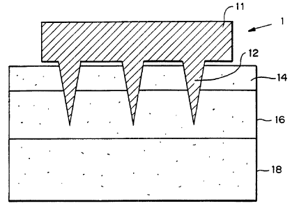
:l0 Figure I is a side elevational view of a schematic of a preferred
embodiment of
the microneedle device inserted into skin. The device 10 includes an upper
portion or
substrate 11 from which a plurality of microneedles 12 protrude. The height of
the upper
portion 11 is between about 1 l,~m and 1 cm, and the width of the upper
portion is between
about 1 mm and 10 em. The upper portion 11 of the device can be solid or
hollow, and
'.l5 may include multiple compartments. In a preferred embodiment for drug
delivery, the
upper portion 11 contains one or more drugs to be delivered. It is also
preferred that the
upper portion include one or more sensors and/or an apparatus (e.g., pump or
electrode)
to drive (provide/direct the force) transport of the drug or other molecules.
The height (or length) of the microneedles 12 generally is between about 1 ~m
20 and I mm. The diameter and length both affect pain as well as functional
properties of
the needles. In transdermal apI>lications, the "insertion depth" of the
microneedles 12 is
preferably less than about 100 lam, more preferably about 30 ~,m, so that
insertion of the
microneedles 12 into the skin through the stratum corneum 14 does not
penetrate past the
epidermis 16 into the dermis lg (as described below), thereby avoiding
contacting nerves
:!5 and reducing the potential for causing pain. In such applications, the
actual length of the
microneedles may be longer, since the portion of the microneedles distal the
tip may not
be inserted into the skin; the uninserted length depends on the particular
device design
and configuration. The actual (overall) height or length of microneedles 12
should be
equal to the insertion depth plus the uninserted length.
:10 The diameter of each microneedle 12 generally is between about 10 nm and 1
mm, and preferably leaves a residual hole (following microneedle insertion and
12
CA 02330207 2000-12-08
WO 99/64580 PCT/US99/13226
withdrawal) of less than about 1 pm, to avoid making a hole which would allow
bacteria
to enter the penetration wound. The actual microneedle diameter should be
larger than 1
p,m, since the hole likely will contract following withdrawal of the
microneedle. The
diameter of microneedle 12 more preferably is between about 1 ~m and 100 p.m.
Larger
diameter and longer microneedles are acceptable, so long as the microneedle
can
penetrate the biological barrier to the desired depth and the hole remaining
in the skin or
other tissue following withdrawal of the microneedle is sufficiently small,
preferably
small enough to exclude bacteriial entry. The microneedles 12 can be solid or
porous, and
can include one or more bores connected to upper portion 11.
l.0 3. Methods of Making Micro~needle Devices
The microneedle devices are made by microfabrication processes, by creating
small mechanical structures in :>ilicon, metal, polymer, and other materials.
These
microfabrication processes are based on well-established methods used to make
integrated circuits, electronic packages and other microelectronic devices,
augmented by
additional methods used in the field of micromachining. The microneedle
devices can
have dimensions as small as a few nanometers and can be mass-produced at low
per-unit
costs.
a. Microfabrication Processes
Microfabrication processes that may be used in making the microneedles
f,0 disclosed herein include lithography; etching techniques, such as wet
chemical, dry, and
photoresist removal; thermal oxidation of silicon; electroplating and
electroless plating;
diffusion processes, such as boron, phosphorus, arsenic, and antimony
diffusion; ion
implantation; film deposition, such as evaporation (filament, electron beam,
flash, and
shadowing and step coverage), sputtering, chemical vapor deposition (CVD),
epitaxy
2.5 (vapor phase, liquid phase, and molecular beam), electroplating, screen
printing,
lamination, stereolithography, laser machining, and laser ablation (including
projection
ablation). See generally Jaeger, Introduction to Microelectronic Fabrication
(Addison-
Wesley Publishing Co., Reading MA 1988); Runyan, et al., Semiconductor
Integrated
Circuit Processing Technology (Addison-Wesley Publishing Co., Reading MA
1990);
3~0 Proceedings of the IEEE Micro Electro Mechanical Systems Conference 1987-
1998; Rai-
13
CA 02330207 2000-12-08
WO 99/64580 PCT/US99/13226
Choudhury, ed., Handbook of Iviicrolithographv. Micromachining &
Microfabrication
(SPIE Optical Engineering Press, Bellingham, WA 1997).
The following methods are preferred for making microneedles.
i. electrochemical etching of silicon
In this method, electrochemical etching of solid silicon to porous silicon is
used to
create extremely fine (on the order of 0.01 ~,m) silicon networks which can be
used as
piercing structures. This method uses electrolytic anodization of silicon in
aqueous
hydrofluoric acid, potentially in combination with light, to etch channels
into the silicon.
By varying the doping concentavation of the silicon wafer to be etched, the
electrolytic
).0 potential during etching, the iinc;ident light intensity, and the
electrolyte concentration,
control over the ultimate pore structure can be achieved. The material not
etched (i.e. the
silicon remaining) forms the miicroneedles. This method has been used to
produce
irregular needle-type structures measuring tens of nanometers in width.
ii. plasma etching
1.5 This process uses deep plasma etching of silicon to create microneedles
with
diameters on the order of 0.1 p.m or larger. Needles are patterned directly
using
photolithography, rather than indirectly by controlling the voltage (as in
electrochemical
etching), thus providing greater control over the final microneedle geometry.
In this process, an appropriate masking material (e.g., metal) is deposited
onto a
silicon wafer substrate and patterned into dots having the diameter of the
desired
microneedles. The wafer is then subjected to a carefully controlled plasma
based on
fluorine/oxygen chemistries to etch very deep, high aspect ratio trenches into
the silicon.
See, e.g., Jansen, et al., "The Black Silicon Method IV: The Fabrication of
Three-
Dimensional Structures in Silicon with High Aspect Ratios for Scanning Probe
5 Microscopy and Other Applications," IEEE Proceedings of Micro Electro
Mechanical
Systems Conference, pp. 88-93 (1995). Those regions protected by the metal
mask
remain and form the needles. 'This method is further described in Example 1
below.
iii. electroplating
In this process, a metal payer is first evaporated onto a planar substrate. A
layer of
~~0 photoresist is then deposited onto the metal to form a patterned mold
which leaves an
exposed-metal region in the shape of needles. By electroplating onto the
exposed regions
14
CA 02330207 2000-12-08
WO 99/64580 PCT/US99/13226
of the metal seed layer, the mold bounded by photoresist can be filled with
electroplated
material. Finally, the substrate and photoresist mold are removed, leaving the
finilshed
microneedle array. The microneedles produced by this process generally have
diameters
on the order of 1 pm or larger. See, e.g., Frazier, et al., "Two dimensional
metallic
microelectrode arrays for extracellular stimulation and recording of neurons",
IEEE
Proceedings of the Micro Elec~'ro Mechanical Systems Conference, pp. I 95-200
( 1993).
iv. other processes
Another method for forming microneedles made of silicon or other materials is
to
use microfabrication techniques such as photolithography, plasma etching, or
laser
:10 ablation to make a mold form (A), transfernng that mold form to other
materials using
standard mold transfer techniques, such as embossing or injection molding (B),
and
reproducing the shape of the oziginal mold form (A) using the newly-created
mold (B) to
yield the final microneedles (C). Alternatively, the creation of the mold form
(A) could
be skipped and the mold (B) could be microfabricated directly, which could
then be used
TS to create the final microneedles~ (C).
Another method of fornaing solid silicon microneedles is by using epitaxial
growth on silicon substrates, as is utilized by Containerless Research, Inc.
(Evanston,
Illinois, USA) for its products.
b. Hollow or Porous Microneedles
~!0 In a preferred embodiment, microneedles are made with pores or other
pathways
through which material may be transported. The following descriptions outline
representative methods for fabricating either porous or hollow microneedles.
i. porous microneedles
Rather than having a single, well-defined hole down the length of the needle,
~;5 porous needles are filled with a network of channels or pores which allow
conduction of
fluid or energy through the needle shaft. It has been shown that by
appropriate
electrochemical oxidation of silicon, pore arrays with high aspect ratios and
a range of
different pore size regimes can be formed; these pore regimes are defined as (
I )
microporous regime with average pore dimensions less than 2 nm, (2) mesoporous
regime
a0 with average pore sizes of betvs~een 2 nm and 50 zun, and (3) macroporous
regime with
pores greater than SO nm. The mesoporous and macroporous regimes are expected
to be
CA 02330207 2000-12-08
WO 99/64580 PCT/US99/13226
most useful for drug delivery. 'Two approaches to porous needles are generally
available,
either (a) the silicon wafer is first made porous and then etched as described
above to
form needles or (b) solid microneedles are etched and then rendered porous,
for example,
by means of electrochemical oxidation, such as by anodization of a silicon
substrate in a
hydrofluoric acid electrolyte. 7.'he size distribution of the etched porous
structure is
highly dependent on several variables, including doping kind and illumination
conditions,
as detailed in Lehmann, "Porou.s Silicon--A New Material for MEMS", IEEE
Proceedings of the Micro Electro Mechanical Systems Conference, pp. 1-6
(1996).
Porous polymer or metallic microneedles can be formed, for example, by
micromolding a
1.0 polymer containing a volatilizalble or teachable material, such as a
volatile salt, dispersed
in the polymer or metal, and thf,n volatilizing or leaching the dispersed
material, leaving a
porous polymer matrix in the shape of the microneedle.
ii. hollow needles
Three-dimensional arrays of hollow rnicroneedles can be fabricated, for
example,
l 5 using combinations of dry etching processes (Laermer, et al., "Bosch Deep
Silicon
Etching: Improving Uniformity and Etch Rate for Advanced MEMS Applications,"
Micro Electro Mechanical Systems, Orlando, Fl, USA, (Jan. 17-21, 1999);
Despont et aL,
"High-Aspect-Ratio, Ultrathick, Negative-Tone Near-UV Photoresist for MEMS",
Proc.
of IEEE 10'h Annual InternatiorTal Workshop on MEMS, Nagoya, Japan, pp. S 18-
522 (Jan.
2;0 26-30, 1997)); micromold creation in lithographically-defined and/or laser
ablated
polymers and selective sidewall. electroplating; or direct micromolding
techniques using
epoxy mold transfers.
One or more distinct and continuous pathways are created through the interior
of
microneedles. In a preferred embodiment, the microneedle has a single annular
pathway
2.5 along the center axis of the microneedle. This pathway can be achieved by
initially
chemically or physically etching the holes in the material and then etching
away
microneedles around the hole. .Alternatively, the microneedles and their holes
can be
made simultaneously or holes can be etched into existing microneedles. As
another
option, a microneedle form or mold can be made, then coated, and then etched
away,
?~0 leaving only the outer coating to form a hollow microneedle. Coatings can
be formed
either by deposition of a film on by oxidation of the silicon microneedles to
a specific
16
CA 02330207 2000-12-08
WO 99/64580 PCT/US99/13226
thickness, followed by removal of the interior silicon. Also, holes from the
backside of
the wafer to the underside of the hollow needles can be created using a front-
to-backside
infrared alignment followed by etching from the backside of the wafer.
a. silicon microneedles
S One method for hollow needle fabrication is to replace the solid mask used
in the
formation of solid needles by a mask that includes a solid shape with one or
more interior
regions of the solid shape removed. One example is a "donut-shaped" mask.
Using this
type of mask, interior regions of the needle are etched simultaneously with
their side
walls. Due to lateral etching of the inner side walls of the needle, this may
not produce
sufficiently sharp walls. In that case, two plasma etches may be used, one to
form the
outer walls of the microneedle (i.e., the 'standard' etch), and one to form
the inner hollow
core (which is an extremely anisotropic etch, such as in inductively-coupled-
plasma
"ICP" etch). For example, the I:C;P etch can be used to form the interior
region of the
needle followed by a second photolithography step and a standard etch to form
the outer
walls of the microneedle. Figure 2a represents a silicon wafer 82 with a
patterned
photoresist layer 84 on top of the wafer 82. The wafer 82 is anisotropically
etched
(Figure 2b) to form a cavity 86 through its entire thickness (Figure 2c). The
wafer 82 is
then coated with a chromium layer 88 followed by a second photoresist layer 90
patterned
so as to cover the cavity 86 and form a circular mask for subsequent etching
(Figure 2d).
The wafer 82 is then etched by ;a standard etch to form the outer tapered
walls 92 of the
microneedle (Figure 2e).
Alternatively, this structure can be achieved by substituting the chromium
mask
used for the solid microneedles described in Example 1 by a silicon nitride
layer 94 on the
silicon substrate 95 covered with chromium 96, deposited as shown in Figure 3a
and
patterned as shown in Figure 3b~. Solid microneedles are then etched as
described in
Example 1 as shown Figure 3c, the chromium 96 is stripped (Figure 3d), and the
silicon
95 is oxidized to form a thin layer of silicon dioxide 97 on all exposed
silicon surfaces
(Figure 3e). The silicon nitride layer 94 prevents oxidation at the needle
tip. The silicon
nitride 94 is then stripped (Figure 3f), leaving exposed silicon at the tip of
the needle and
oxide-covered silicon 97 everywhere else. The needle is then exposed to an ICP
plasma
17
CA 02330207 2000-12-08
WO 99/64580 PCT/US99/13226
which selectively etches the inr.~er sidewalls of the silicon 95 in a highly
anisotropic
manner to form the interior hole of the needle (Figure 3g).
Another method uses the solid silicon needles described previously as 'forts'
around which the actual needle structures are deposited. After deposition, the
forms are
etched away, yielding the hollow structures. Silica needles or metal needles
can be
formed using different methods. Silica needles can be formed by creating
needle
structures similar to the ICP neE:dles described above prior to the oxidation
described
above. The wafers are then oxidized to a controlled thickness, forming a layer
on the
shaft of the needle form which will eventually become the hollow microneedle.
The
silicon nitride is then stripped and the silicon core selectively etched away
(e.g., in a wet
alkaline solution) to form a hollow silica microneedle.
In a preferred embodimc;nt, an array of hollow silicon microtubes is made
using
deep reactive ion etching combined with a modified black silicon process in a
conventional reactive ion etches, as described in Example 3 below. First,
arrays of
circular holes are patterned through photoresist into Si02 , such as on a
silicon wafer.
Then the silicon can be etched using deep reactive ion etching (DRIE) in an
inductively
coupled plasma (ICP) reactor to etch deep vertical holes. The photoresist was
then
removed. Next, a second photolithography step patterns the remaining Si02
layer into
circles concentric to the holes, leaving ring shaped oxide masks surrounding
the holes.
The photoresist is then removedl and the silicon wafer again deep silicon
etched, such that
the holes are etched completely through the wafer (inside the Si02 ring) and
simultaneously the silicon is etched around the Si02 ring leaving a cylinder.
This latter process can be varied to produce hollow, tapered microneedles.
After
an array of holes is fabricated as described above, the photoresist and Si02
layers are
replaced with conformal DC sputtered chromium rings. The second ICP etch is
replaced
with a SF6/02 plasma etch in a reactive ion etches (RIE), which results in
positively
sloping outer sidewalls. Henry, et al., "Micromachined Needles for the
Transdermal
Delivery of Drugs," Micro Electro Mechanical Systems, Heidelberg, Germany, pp.
494-
498 (Jan. 26-29, 1998).
18
CA 02330207 2000-12-08
WO 99/64580 PCT/US99/13226
b. metal ,mieroneedles
Metal needles can be foamed by physical vapor deposition of appropriate metal
layers on solid needle forms, which can be made of silicon using the
techniques described
above, or which can be formed using other standard mold techniques such as
embossing
or injection molding. The metals are selectively removed from the tips of the
needles
using electropolishing techniques, in which an applied anodic potential in an
electrolytic
solution will cause dissolution of metals more rapidly at sharp points, due to
concentration of electric field lines at the sharp points. Once the underlying
silicon
needle forms have been exposed at the tips, the silicon is selectively etched
away to form
hollow metallic needle structurca. This process could also be used to make
hollow
needles made from other materials by depositing a material other than metal on
the needle
forms and following the procedure described above.
A preferred method of fabricating hollow metal microneedles utilizes micromold
plating techniques, which are dfacribed as follows and in Examples 4 and S. In
a method
for making metal microtubes, which does not require dry silicon etching, a
photo-defined
mold first is first produced, for .example, by spin casting a thick layer,
typically 1 SO lun,
of an epoxy (e.g., SU-8) onto a substrate that has been coated with a thin
sacrificial layer,
typically about 10 to 50 nm. .A~xays of cylindrical holes are then
photolithographieally
defined through the epoxy layer, which typically is about 150 p,m thick.
(Despont, et al.,
"High-Aspect-Ratio, Ultrathick, Negative-Tone Near-UV Photoresist fox MEMS,'''
Proc.
of IEEE 10'h Annual International Workshop on MEMS, Nagoya, Japan, pp. 518-522
(Jan.
26-30, 1997)). The diameter of these cylindrical holes defines the outer
diameter of the
tubes. The upper surface of the substrate, the sacrificial layer, is then
partially removed at
the bottom of the cylindrical holes in the photoresist. The exact method
chosen depends
on the choice of substrate. For example, the process has been successfully
performed on
silicon and glass substrates (in which the upper surface is etched using
isotropic wet or
dry etching techniques) and copper-clad printed wiring board substrates. In
the latter
case, the copper laminate is selectively removed using wet etching. Then a
seed layer,
such as Ti/Cu/Ti (e.g., 30 nm/21)0 nm/30 nm), is conformally DC sputter-
deposited onto
the upper surface of the epoxy mold and onto the sidewalls of the cylindrical
holes. The
seed layer should be electrically isolated from the substrate. Subsequently,
one or more
19
CA 02330207 2000-12-08
WO 99/64580 PCT/US99/13226
electroplatable metals or alloys, such as Ni, NiFe, Au, Cu, or Ti, are
electroplated onto
the seed layer. The surrounding epoxy is then removed, leaving microtubes
which each
have an interior annular hole that extends through the base metal supporting
the tubes.
The rate and duration of electra~plating is controlled in order to define the
wall thickness
and inner diameter of the micro~tubes. In one embodiment, this method was used
to
produce microtubes having a hc;ight of between about 150 and 250 pm, an outer
diameter
of between about 40 and 120 ~Cm, and an inner diameter of between about 30 and
110 ~m
(i.e., having a wall thickness of 10 p,m). In a typical array, the microtubes
have a tube
center-to-center spacing of about 150 p,m, but can vary depending on the
desired needle
l.0 density.
A variation of this method is preferred for forming tapered microneedles. .As
described above, photolithography yields holes in the epoxy which have
vertical
sidewalls, such that the resulting shafts of the microneedles are straight,
not tapered. This
vertical sidewall limitation can be overcome by molding a preexisting 3D
structure, i.e., a
mold-insert. The subsequent removal of the mold-insert leaves a mold which can
be
surface plated similarly to the holes produced by photolithography described
above.
Alternatively, non-vertical sidewalk can be produced directly in the polymeric
mold into which electroplating will take place. For example, conventional
photoresists
known in the art can be exposed and developed in such as way as to have the
surface
2;0 immediately adjacent to the mask be wider than the other surface.
Specialized greyscale
photoresists in combination with greyscale masks can accomplish the same
effect. Laser-
ablated molds can also be made: with tapered sidewalk, e.g., by optical
adjustment of the
beam (in the case of serial hole fabrication) or of the reticle or mold during
ablation (in
the case of projection ablation).
Z;5 To form hollow tapered microneedles, the mold-insert is an array of solid
silicon
microneedles, formed as described in Henry, et al., "Micromachined Needles for
the
Transdermal Delivery of Drugs;'" Micro Electro Mechanical Systems, Heidelberg,
Germany, Jan. 26-29, pp. 494-498 (1998). First, a layer of a material, such as
an epoxy
(e.g., SU-8 or a polydimethylsil.oxane ("PDMS")), is spin cast onto the array
of silicon
?~0 microneedles to completely blanket the entire array. 'the epoxy settles
during pre-bake to
CA 02330207 2000-12-08
WO 99/64580 PCT/US99/13226
create a planar surface above the silicon needle tips; the material is then
fully pre-baked,
photolithographically cross-linls;ed, and post-baked.
The upper surface of the: epoxy is then etched away, for example with an
02/CHF3
plasma, until the needle tips are exposed, preferably leaving between about 1
and S p,m of
tip protruding from the epoxy. 'The silicon is then selectively removed, for
example by
using a SF6 plasma or a HN03/13F solution. The remaining epoxy micromold is
the
negative of the microneedles and has a small diameter hole where the tip of
the
microneedle formerly protruded.
After the removal of the silicon, a seed layer, such as Ti-Cu-Ti, is
conformally
sputter-deposited onto the epoxy micromold. Following the same process
sequence
described for hollow metal microtubes, one or more electroplatable metals or
alloys, such
as Ni, NiFe, Au, or Cu, are electroplated onto the seed layer. Finally, the
epoxy is
removed, for example by using .an 02/CHF3 plasma, leaving an array of hollow
metal
microneedles. An advantage of using PDMS in this application is that the
micromold can
be physically removed from the silicon mold insert by mechanical means, such
as
peeling, without damaging the silicon mold insert, thus allowing the silicon
mold insert to
be reused. Furthermore, the electroplated microneedles can be removed from the
PDMS
mold by mechanical means, for example by peeling, thereby allowing the PDMS to
also
be reused. In a preferred embodliment, this method is used to produce
microneedles
2'0 having a height of between about 150 and 250 p,m, an outer diameter of
between about 40
and 120 ~tm, and an inner diameter of between about 50 and 100 p,m. In a
typical array,
the microtubes have a tube centc,r-to-center spacing of about 150 Vim, but can
vary
depending on the desired needle density. The microneedles are 150 ~m in height
with a
base diameter of $0 p,m, a tip di,~neter of 10 p,m, and a needle-to-needle
spacing of 1 SO
2.5 pm.
c. silicon dioxide microneedles
Hollow microneedles formed of silicon dioxide can be made by oxidizing the
surface of the silicon microneedle forms (as described above), rather than
depositing a
metal and then etching away the solid needle forms to leave the hollow silicon
dioxide
30 structures. This method is illustrated in Figures 4a-4d. Figure 4a shows an
array 24 of
needle forms 26 with masks 28 on their tips. In Figure 4b, the needle forms 26
have been
21
CA 02330207 2000-12-08
WO 99/64580 PCT/US99/13226
coated with a layer 30 of metal, silicon dioxide or other material. Figure 4c
shows the
coated needle forms 26 with the: masks 28 removed. Finally, in Figure 4d, the
needle
forms 26 have been etched away, leaving hollow needles 30 made of metal,
silicor<
dioxide, or other materials.
In one embodiment, hollow, porous, or solid microneedles are provided with
longitudinal grooves or other modifications to the exterior surface of the
microneedles.
Grooves, for example, should be useful in directing the flow of molecules
along the
outside of microneedles.
d. op Iyme~r microneedles
In a preferred method, polymeric microneedles are made using microfabricated
molds. For example, the epoxy molds can be made as described above and
injection
molding techniques can be appliied to form the microneedles in the molds
(Weber, et al.,
"Micromolding - a powerful tool for the large scale production of precise
microstructures", Proc. SPIE - International Soc. Optical Engineer. 2879, 156-
167 (1996);
Schift, et al., "Fabrication of replicated high precision insert elements for
micro-optical
bench arrangements" Proc. SPIN - International Soc. Optical Engineer. 3513,
122-134
(1998). These micromolding techniques are preferred over other techniques
described
herein, since they can provide relatively less expensive replication, i.e.
lower cost of mass
production. In a preferred embodiment, the polymer is biodegradable.
2~D 4. Microneedle Device Applications
The device may be used for single or multiple uses for rapid transport across
a
biological barrier or may be left in place for longer times (e.g., hours or
days) for long-
term transport of molecules. Depending on the dimensions of the device, the
application
site, and the route in which the device is introduced into (or onto) the
biological barrier,
2.5 the device may be used to introdluce or remove molecules at specific
locations.
As discussed above, Figure 1 shows a side elevational view of a schematic of a
preferred embodiment of the mi~,roneedle device 10 in a transdermal
application. The
device 10 is applied to the skin such that the microneedles 12 penetrate
through the
stratum corneum and enter the viable epidermis so that the tip of the
microneedle at least
3~D penetrates into the viable epidermis. In a preferred embodiment, drug
molecules in a
reservoir within the upper portion 11 flow through or around the microneedles
and into
22
CA 02330207 2000-12-08
WO 99/64580 PCT/US99/13226
the viable epidermis, where the drug molecules then diffuse into the dermis
for local
treatment or for transport through the body.
To control the transport of material out of or into the device through the
microneedles, a variety of forcea or mechanisms can be employed. These include
S pressure gradients, concentration gradients, electricity, ultrasound,
receptor binding, heat,
chemicals, and chemical reactions. Mechanical or other gates in conjunction
with the
forces and mechanisms describE:d above can be used to selectively control
transport of the
material.
In particular embodiments, the device should be "user-friendly." For example,
in
some transdermal applications, affixing the device to the skin should be
relatively simple,
and not require special skills. This embodiment of a microneedle may include
an array of
microneedles attached to a housing containing drug in an internal reservoir,
wherein the
housing has a bioadhesive coating around the microneedles. The patient can
remove a
peel-away backing to expose an adhesive coating, and then press the device
onto a clean
IS part of the skin, leaving it to administer drug over the course of, for
example, several
days.
a. Drug Delivery
Essentially any drug or other bioactive agents can be delivered using these
devices. Drugs can be proteins, enzymes, polysaccharides, polynucleotide
molecules, and
synthetic organic and inorganic compounds. Representative agents include anti-
infectives, hormones, such as insulin, growth regulators, drugs regulating
cardiac action
or blood flow, and drugs for pain control. The drug can be for local treatment
or for
regional or systemic therapy. The following are representative examples, and
disorders
they are used to treat:
Calcitonin, osteoporosis; Enoxaprin, anticoagulant; Etanercept, rheumatoid
arthritis; Erythropoietin, anemia; Fentanyl, postoperative and chronic pain;
Filgrastin, low
white blood cells from chemotherapy; Heparin, anticoagulant; Insulin, human,
diabetes;
Interferon Beta 1 a, multiple sclerosis; Lidocaine, local anesthesia;
Somatropin, growth
hormone; and Sumatriptan, migraine headaches.
In this way, many drugs can be delivered at a variety of therapeutic rates.
The rate
can be controlled by varying a number of design factors, including the outer
diameter of
23
CA 02330207 2000-12-08
WO 99/64580 PCT/US99/13226
the microneedle, the number and size of pores or channels in each microneedle,
the
number of microneedles in an array, the magnitude and frequency of application
of the
force driving the drug through the microneedle and/or the holes created by the
microneedles. For example, devices designed to deliver drug at different rates
might have
more microneedles for more rapid delivery and fewer microneedles for less
rapid
delivery. As another example, a device designed to deliver drug at a variable
rate could
vary the driving force (e.g., preasure gradient controlled by a pump) for
transport
according to a schedule which 'was pre-programmed or controlled by, for
example, the
user or his doctor. The devices can be affixed to the skin or other tissue to
deliver drugs
:LO continuously or intermittently, for durations ranging from a few seconds
to several hours
or days.
One of skill in the art can measure the rate of drug delivery for particular
microneedle devices using in mstro and in vivo methods known in the art. For
example, to
measure the rate of transdermal drug delivery, human cadaver skin mounted on
standard
:l5 diffusion chambers can be usedl to predict actual rates. See Hadgraft &
Guy, eds.,
Transdermal Drug Delivery: Developmental Issues and Research Initiatives
(Marcel
Dekker, New York 1989); Bronaugh & Maibach, Percutaneous Absorption,
Mechanisms-
-Methodol~;,v--Drug Delivery (Marcel Dekker, New York 1989). After filling the
compartment on the dermis side of the diffusion chamber with saline, a
microneedle array
:!0 is inserted into the stratum corneum; a drug solution is placed in the
reservoir of the
microneedle device; and samples of the saline solution are taken over time and
assayed to
determine the rates of drug transport.
In an alternate embodiment, biodegradable or non-biodegradable microneedles
can be used as the entire drug delivery device, where biodegradable
microneedles are a
:!5 preferred embodiment. For ex~unple, the microneedles may be formed of a
biodegradable
polymer containing a dispersion of an active agent for local or systemic
delivery. The
agent could be released over tune, according to a profile determined by the
composition
and geometry of the microneedles, the concentration of the drug and other
factors. In this
way, the drug reservoir is within the matrix of one or more of the
microneedles.
;10 In another alternate embodiment, these microneedles may be purposefully
sheared
off from the substrate after penetrating the biological barrier. In this way,
a portion of the
24
CA 02330207 2000-12-08
WO 99/64580 PCT/US99/13226
microneedles would remain within or on the other side of the biological
barrier and a
portion of the microneedles and their substrate would be removed from the
biological
barner. In the case of skin, this could involve inserting an array into the
skin, manually or
otherwise breaking off the microneedles tips and then remove the base of the
microneedles. The portion of the microneedles which remains in the skin or in
or across
another biological barrier could then release drug over time according to a
profile
determined by the composition and geometry of the microneedles, the
concentration of
the drug and other factors. In a~ preferred embodiment, the microneedles are
made of a
biodegradable polymer. The release of drug from the biodegradable microneedle
tips can
:l0 be controlled by the rate of polymer degradation. Microneedle tips can
release drugs for
local or systemic effect, or othc;r agents, such as perfume, insect repellent
and sun block.
Microneedle shape and content can be designed to control the breakage of
microneedles. For example, a notch can be introduced into microneedles either
at the
time of fabrication or as a subsequent step. In this way, microneedles would
:l5 preferentially break at the site of the notch. Moreover, the size and
shape of the portion of
microneedles which break off c;an be controlled not only for specific drug
release
patterns, but also for specific interactions with cells in the body. For
example, objects of
a few microns in size are known to be taken up by macrophages. The portions of
microneedles that break off carp be controlled to be bigger or smaller than
that to prevent
:'0 uptake by macrophages or can be that size to promote uptake by
macrophages, which can
be desirable for delivery of vaccines.
b. Dia nostic Sensing of Body Fluids (Biosensors~
One embodiment of the devices described herein may be used to remove material
from the body across a biological barrier, i.e. for minimally invasive
diagnostic sensing.
5 For example, fluids can be transported from interstitial fluid in a tissue
into a reservoir in
the upper portion of the device.. The fluid can then be assayed while in the
reservoir or
the fluid can be removed from the reservoir to be assayed, for diagnostic or
other
purposes. For example, interstitial fluids can be removed from the epidermis
across the
stratum corneum to assay for glucose concentration, which should be useful in
aiding
:30 diabetics in determining their required insulin dose. Other substances or
properties that
would be desirable to detect ine:lude lactate (important for athletes),
oxygen, pH, alcohol,
CA 02330207 2000-12-08
WO 99/64580 PCT/US99/13226
tobacco metabolites, and illegal drugs (important for both medical diagnosis
and law
enforcement).
The sensing device can be in or attached to one or more microneedles, or in a
housing adapted to the substrate. Sensing information or signals can be
transferred
optically (e.g., refractive index) or electrically (e.g., measuring changes in
electrical
impedance, resistance, current, voltage, or combination thereof). For example,
it may be
useful to measure a change as a function of change in resistance of tissue to
an electrical
current or voltage, or a change in response to channel binding or other
criteria (such as an
optical change) wherein different resistances are calibrated to signal that
more or less
:l0 flow of drug is needed, or that delivery has been completed.
In one embodiment, onE: or more microneedle devices can be used for (1)
withdrawal of interstitial fluid, (2) assay of the fluid, and/or (3) delivery
of the
appropriate amount of a therapeutic agent based on the results of the assay,
either
automatically or with human intervention. For example, a sensor delivery
system may be
:l5 combined to form, for example, a system which withdraws bodily fluid,
measures its
glucose content, and delivers a~i appropriate amount of insulin. The sensing
or delivery
step also can be performed using conventional techniques, which would be
integrated into
use of the microneedle device. For example, the microneedle device could be
used to
withdraw and assay glucose, arid a conventional syringe and needle used to
administer the
:?0 insulin, or vice versa.
In an alternate embodiment, microneedles may be purposefully sheared off from
the substrate after penetrating tike biological barrier, as described above.
The portion of
the microneedles which remain within or on the other side of the biological
barrier could
contain one or more biosensors. For example, the sensor could change color as
its output.
5 For microneedles sheared off in the skin, this color change could be
observed through the
skin by visual inspection or with the aid of an optical apparatus.
Other than transport of drugs and biological molecules, the microneedles rnay
be
used to transmit or transfer other materials and energy forms, such as light,
electricity,
heat, or pressure. The microneedles, for example, could be used to direct
light to specific
;30 locations within the body, in order that the light can directly act on a
tissue or on an
intermediary, such as light-sen:>itive molecules in photodynamic therapy. The
26
CA 02330207 2000-12-08
WO 99/64580 PCT/US99/13226
microneedles can also be used for aerosolization or delivery for example
directly to a
mucosal surface in the nasal or buccal regions or to the pulmonary system.
The microneedle devices disclosed herein also should be useful for controlling
transport across tissues other than skin. For example, microneedles can be
inserted into
the eye across, for example, conjunctiva, sclera, and/or cornea, to facilitate
delivery of
drugs into the eye. Similarly, microneedles inserted into the eye can
facilitate transport of
fluid out of the eye, which may be of benefit for treatment of glaucoma.
Microneedles
may also be inserted into the bu~ccal (oral), nasal, vaginal, or other
accessible mucosa to
facilitate transport into, out of, or across those tissues. For example, a
drug may be
l.0 delivered across the buccal muc;osa for local treatment in the mouth or
for systemic
uptake and delivery. As another example, microneedle devices may be used
internally
within the body on, for example, the lining of the gastrointestinal tract to
facilitate uptake
of orally-ingested drugs or the lining of blood vessels to facilitate
penetration of drugs
into the vessel wall. For examfde, cardiovascular applications include using
microneedle
l.5 devices to facilitate vessel distension or immobilization, similarly to a
stmt, wherein the
microneedles/substrate can function as a "staple-like" device to penetrate
into different
tissue segments and hold their relative positions for a period of time to
permit tissue
regeneration. This application could be particularly useful with biodegradable
devices.
These uses may involve invasive procedures to introduce the microneedle
devices into the
~:0 body or could involve swallowing, inhaling, injecting or otherwise
introducing the
devices in a non-invasive or minimally-invasive manner.
The present invention will be further understood with reference to the
following
non-limiting examples.
Example 1: Fabrication of Sa~lid Silicon Microneedles
2:5 A chromium masking miaterial was deposited onto silicon wafers and
patterned
into dots having a diameter approximately equal to the base of the desired
microneedles.
The wafers were then loaded into a reactive ion etcher and subjected to a
carefully
controlled plasma based on fluorine/oxygen chemistries to etch very deep, high
aspect
ratio valleys into the silicon. Tlhose regions protected by the metal mask
remain and form
?~0 the microneedles.
27
CA 02330207 2000-12-08
WO 99/64580 PCT/US99/13226
<100>-oriented, prime grade, 450-550 ~m thick, 10-15 S2-cm silicon wafers
(Nova Electronic Materials Tnc;., Richardson, TX) were used as the starting
material. The
wafers were cleaned in a solutiion of 5 parts by volume deionized water, 1
part 30%
hydrogen peroxide, and 1 part 30% ammonium hydroxide (J.T. Baker,
Phillipsburg, NJ)
at approximately 80°C for 15 minutes, and then dried in an oven (Blue M
Electric,
Watertown, WI) at 150°C for 10 minutes. Approximately 1000 A of
chromium (Mat-Vac
Technology, Flagler Beach, FL) was deposited onto the wafers using a DC-
sputterer (601
Sputtering System, CVC Products, Rochester, NY). The chromium layer was
patterned
into 20 by 20 arrays of 80 pm .diameter dots with 150 p,m center-to-center
spacing using
the lithographic process described below.
A layer of photosensitive material (1827 photoresist, Shipley, Marlborough,
MA)
was deposited onto the chromium layer covering the silicon wafers. A standard
lithographic mask (Telic, Santa Monica, CA) bearing the appropriate dot array
pattern
was positioned on top of the photoresist layer. The wafer and photoresist were
then
exposed to ultraviolet (UV) light through the mask by means of an optical mask
aligner
(Hybralign Series 500, Optical Associates, Inc., Milpitas, CA). The exposed
photoresist
was removed by soaking the wafers in a liquid developer (354 developer,
Shipley,
Marlborough, MA) leaving the: desired dot array of photoresist on the chromium
layer.
Subsequently, the wafers were dipped into a chromium etchant (CR-75; Cyanteck:
Fremont, CA), which etched the chromium that had been exposed during the
photolithography step, leaving dot arrays of chromium (covered with
photoresist) on the
surface of the silicon wafer. The photoresist still present on the chromium
dots formed
the masks needed for fabrication of the microneedles, described below.
The microneedles were fabricated using a reactive ion etching techniques based
.25 on the Black Silicon Method developed at the University of Twente. The
patterned
wafers were etched in a reactive ion etcher (700 series wafer/batch Plasma
Processing
System, Plasma Therm, St. Petersburg, FL) with means for ensuring good thermal
contact
between the wafers and the underlying platen (Apiezon N, K.J. Lesker,
Clairton, PA).
The wafers were etched using the following gases and conditions: SF6 (20
standard cubic
centimeters per minute) and O > ( 15 standard cubic centimeters per minute) at
a pressure
of 150 mTorr and a power of 150 W for a run time of approximately 250 minutes.
These
28
CA 02330207 2000-12-08
WO 99/64580 PCT/US99/13226
conditions caused both deep vertical etching and slight lateral underetching.
By
controlling the ratio of flow rates of the SF6 and 02 gases used to form the
plasma, the
aspect ratio of the microneedles could be adjusted. The regions protected by
the
chromium masks remained and formed the microneedles. Etching was allowed to
proceed until the masks fell off' due to underetching, resulting in an array
of sharp silicon
spikes.
Example 2: Transdermal Transport Using Solid Microneedles
To determine if microfa.bricated microneedles could be used to enhance
transdermal drug delivery, axra;ys of microneedles were made using a deep
plasma etching
J.0 technique. Their ability to penc;trate human skin without breaking was
tested and the
resulting changes in transderma~l transport were measured.
Arrays of microneedles were fabricated having extremely sharp tips (radius of
curvature less than 1 pm), and are approximately 150 pm long. Because the skin
surface
is not flat due to dermatoglyphics and hair, the full length of these
microneedles will not
l.5 penetrate the skin. All experiments were performed at room temperature
(232°C).
The ability of the microneedles to pierce skin without breaking was then
tested.
Insertion of the arrays into skin required only gentle pushing. Inspection by
light and
electron microscopy showed that more than 95% of microneedles within an array
pierced
across the stratum corneum of the epidermis samples. Moreover, essentially all
of the
~;0 microneedles that penetrated the epidermis remained intact. On those very
few which
broke, only the top 5-10 p,m wa.s damaged. Microneedle arrays could also be
removed
without difficulty or additional damage, as well as re-inserted into skin
multiple times.
To quantitatively assess the ability of microneedles to increase transdermal
transport, calcein permeability of human epidermis with and without inserted
microneedle
2;5 arrays was measured. Calcein crosses skin very poorly under normal
circumstances and
therefore represents an especially difficult compound to deliver. As expected,
passive
permeability of calcein across unaltered skin was very low, indicating that
the epidermis
samples were intact.
Insertion of microneedlc;s into skin was capable of dramatically increasing
?~0 permeability to calcein. When microneedles were inserted and left embedded
in the skin,
calcein permeability was increased by more than 1000-fold. Insertion of
microneedles for
29
CA 02330207 2000-12-08
WO 99/64580 PCTNS99/13226
s, followed by their removal, yielded an almost 10,000-fold increase. Finally,
insertion of a microneedle array for 1 h, followed by its removal, increased
skin
permeability by about 25,000-i:old. Permeabilities for skin with microneedles
inserted
and then removed are higher tr~an for skin with microneedles remaining
embedded
5 probably because the micronee;dles themselves or the silicon plate
supporting the array
may block access to the micro:ecopic holes created in the skin. Light
microscopy showed
that the holes which remained :in the skin after microneedles were removed
were
approximately 1 ~m in size.
To confirm in vitro experiments which showed that skin permeability can be
10 significantly increased by microneedles, studies were conducted with human
volunteers.
They indicated that microneedl',es could be easily inserted into the skin of
the forearm or
hand. Moreover, insertion of nnicroneedle arrays was never reported to be
painful, but
sometimes elicited a mild "we~~ring" sensation described as a weak pressure or
the feeling
of a piece of tape affixed to the: skin. Although transport experiments were
not performed
in vivo, skin electrical resistance was measured before and after microneedle
insertion.
Microneedles caused a 50-fold drop in skin resistance, a drop similar to that
caused by the
insertion of a 30-gauge "macroneedle." Inspection of the site immediately
after
microneedle insertion showed no holes visible by light microscopy. No
erythema, edema,
or other reaction to microneedles was observed over the hours and days which
followed.
:20 This indicates that microneedle; arrays can permeabilize skin in human
subjects in a non-
painful and safe manner.
Example 3: Fabrication of Silicon Microtubes
Three-dimensional arrays of rnicrotubes were fabricated from silicon, using
deep
reactive ion etching combined with a modified black silicon process in a
conventional
:25 reactive ion etcher. The fabrication process is illustrated in Figures Sa-
d. First, arrays of
40 pm diameter circular holes 32 were patterned through photoresist 34 into a
1 pm thick
Si02 layer 36 an a two inch siliicon wafer 38 (Figure Sa). The wafer 38 was
then etched
using deep reactive ion etching; (DRIE) (Laermer, et al., "Bosch Deep Silicon
Etching:
Improving Uniformity and Etclh Rate for Advanced MEMS Applications," Micro
Electro
30 Mechanical Systems, Orlando, Florida, USA (Jan. 17-21, 1999)). in an
inductively
coupled plasma (ICP) reactor to etch deep vertical holes 40. The deep silicon
etch was
CA 02330207 2000-12-08
WO 99/64580 PCT/US99/13226
stopped after.the holes 40 are approximately 200 ~m deep into the silicon
substrate 38
(Figure Sb) and the photoresist 34 was removed. A second photolithography step
patterned the remaining Si02 layer 36 into circles concentric to the holes,
thus leaving
ring shaped oxide masks 34 swTOUnding the holes (Figure Sc). The photoresist
34 was
then removed and the wafer 38 was again deep silicon etched, while
simultaneously the
holes 40 were etched completely through the wafer 38 (inside the SiOZ ring)
and the
silicon was etched around the Si02 ring 38 leaving a cylinder 42 (Figure Sd).
The
resulting tubes were 150 pm in height, with an outer diameter of 80 Vim, an
inner
diameter of 40 pm, and a tube center-to-center spacing of 300 N.m.
l.0 Example 4: Micromold Fabrication of Metal Microtubes
Hollow metal microtubes were prepared without dry silicon etching, using a
thick,
photo-defined mold of epoxy. 'The sequences are illustrated in Figures 6a-e.
First, a thick
layer of SU-8 epoxy 44 was spin cast onto a silicon or glass substrate 46 that
had been
coated with 30 nm of titanium 48, the sacrificial layer. Arrays of cylindrical
holes 49
l.5 were then photolithographically defined through an epoxy layer 44,
typically 150 ~m
thick (Figure 6a). The sacrificial layer then was partially removed using a
wet etching
solution containing hydrofluoric acid and water at the bottom of the
cylindrical holes in
the SU-8 photoresist 46 (Figure: 6b). A seed layer of Ti/Cu/Ti (30 nm/200
nm/30 nm) 39
was then conformally DC sputter-deposited onto the upper surface of the epoxy
mold and
20 onto the sidewalls of the cylindrical holes 49 (Figure 6c). As shown in
Figure 6c, the
seed layer 39 was electrically isolated from the substrate. Subsequently, NiFe
was
electroplated onto the seed layer 39 (Figure 6d), the epoxy 44 was removed
from the
substrate, and the surrounding epoxy 44 was removed (Figure 6e). The resulting
microtubes are 200 pm in height with an outer diameter of 80 Vim, an inner
diameter of 60
2.5 pm, and a tube center-to-center spacing of 150 p,m. T'he holes in the
interior of the
microtubes protrude through the base metal supporting the tubes.
Example 5: Micromold Fabrication of Tapered Microneedles
A micromold having tapered walls was fabricated by molding a preexisting 3-D
array of microneedles, i.e. the mold-insert, and subsequently removing the
mold insert.
?'~0 The micromold was then surface plated in a manner similar to that for the
microtubes
described in Example 4. The fabrication sequence is illustrated in Figures 7a-
7d.
31
CA 02330207 2000-12-08
WO 99/64580 PCT/US99/13226
First, an array of solid silicon microneedles 50 were prepared as described in
Henry, et al., "Micromachined Needles for the Transdermal Delivery of Drugs,"
Micro
Electro Mechanical Systems, Hfeidelberg, Germany, Jan. 26-29, pp. 494-498
(1998).
Then, a layer of epoxy 52 (SU-8) was spin cast onto the microneedle array to
completely
blanket the array (Figure 7a). 'Che epoxy 52 settled during pre-bake to create
a planar
surface above the tips of the miicroneedles 50. The epoxy 52 was then fully
pre-baked,
photolithographically cross-linlked, and post-baked.
Then, the upper surface of the epoxy 52 was etched away using an O2/CHF3
plasma until approximately 1 to 2 p,m of the needle tips 54 were exposed,
protruding from
a0 the epoxy 52 (Figure 7b). The silicon was then selectively removed by using
a SF6
plasma (Figure 7c). The remaining epoxy mold 52 provided a negative of the
microneedles with a small diameter hole where the tip of the silicon needle
protruded.
After the removal of the silicon, a seed layer of Ti-Cu-Ti 54 was conformally
sputter-
deposited onto the top and sidewalk of the epoxy micromold 52. Following the
same
:l5 process sequence as described iin Example 4, NiFe was then electroplated
onto the seed
layer 54 (Figure 7c). Finally, tlhe epoxy was removed using an Oz/CHF3 plasma,
leaving
a 20 x 20 array of NiFe hollow metal microneedles 54 (Figure 7d). The
microneedles 54
were 1 SO p.m in height with a base diameter of 80 p,m, a tip diameter of 10
Vim, and a
needle-to-needle spacing of 151) pm.
20 Micromold-based microneedles also have been successfully manufactured using
a
process in which the epoxy mold material was replaced with PDMS. In this case,
it was
possible to remove the mold from the mold insert, as well as the microneedles
from the
mold, using only physical techniques such as peeling. This approach
advantageously
requires no dry etching and allows one to reuse both the mold and the mold
insert.
25 Example 6: Micromold Fabrication of Tapered Microneedles Using
Laser-Formed Molds
A micromold having tapered walls was fabricated by use of laser ablation
techniques, as shown in Figurea 8a-d. A laser-ablatable polymer sheet 60 such
as
KAPTONTM polyimide approximately 150 microns in thickness was optionally
laminated
;30 to a thin (10-30 micron) metal sheet 62 such as titanium (Figure 8a). A
tapered hole 64
was formed in the metal/polymer laminate 60/62 using a laser technique such as
excimer
32
CA 02330207 2000-12-08
WO 99/64580 PC'T/US99/13226
laser ablation,(Figure 8b). The entry hole of the laser spot was on the metal
side 62, and a
through hole was made through. both the metal sheet and the polymer film. The
through
hole 64 was tapered in combination with either defocusing or appropriate
substrate
motion to create a taper such that the wide end of the hole 64 (typically 40-
50 microns)
was on the metal side 62 and the narrow end of the hole 64 (typically 10-20
microns) was
on the polymer 60 side. A thin layer of metal 66, e.g. titanium, of thickness
0.1 micron
was then deposited, e.g., using a sputter-deposition technique, in such a way
that the
metal 66 deposited on the metal. film side and coated the polymer sidewalls,
but did not
coat the polymer 60 side of the laminate (Figure 8c). Electrodeposition of
metal 68, e.g.,
gold, to a thickness of 1 to 5 microns was then performed on the titanium-
coated metal
surface 66, and polymer sidewalls curved section of 60 next to 64. Finally,
the polymer
60 was removed, using e.g. an oxygen plasma, to form the completed
microneedles
(Figure 8d).
Alternate polymer removal methods, such as thermal, solvent, aqueous, or photo-
degradation followed by solvent or aqueous removal, are also possible if the
polymer
material is chosen appropriately (e.g., a photoresist resin).
Example 7: Formation of Mi~.roneedles by Embossing
Formation of a micronee;dle by embossing is shown in Figures 9a-9f. A
polymeric
layer 70 (Figure 9a) is embossed by a solid microneedle or microneedle array
72 (F figure
9b). The array 72 is removed (Figure 9c), and the layer 70 is etched from the
non-
embossed side 74 until the embossed cavity 76 is exposed (Figure 9d). A
metallic layer
78 is then deposited on the embossed side and the sidewalls, but not on the
non-embossed
side 74 (Figure 9e). This layer '78 is optionally thickened by
electrodeposition of an
additional metal layer 80 on top of it (Figure 9e). The polymer layer 70 is
then removed
to form the microneedles 78/80 (Figure 9f).
Example 8: Transdermal Application of Hollow Microneedles
The bore of hollow microneedles must provide fluid flow with minimal clogging
in order to be suitable to transport material, such as in transdermal drug
delivery.
Therefore, microneedles and microtubes were evaluated to determine their
suitability for
these functions.
33
CA 02330207 2000-12-08
WO 99/64580 PCT/US99/13226
Hollow metal and silicon microneedles, produced as described in Examples 3-5,
were inserted through human skin epidermis with no apparent clogging of the
needle
bores. Scanning electron microscopy of a hollow metal (NiFe) microneedle
penetrating
up through the underside of hurnan epidermis showed the microneedle remains
intact,
with the tip free of debris. Simiilarly, silicon microneedles, metal
microneedles, and metal
microtubes were successfully ir.~serted through human skin. Also, the hollow
microneedles were shown to permit the flow of water through their bores.
Example 9: Drug Transporit Through Microneedles Inserted Into Skin
Studies were performed with solid and hollow microneedles to demonstrate
transport of molecules and fluidls. As shown in Table 1, transport of a number
of different
compounds across skin is possible using microneedles. These studies were
performed
using either solid silicon microneedles or using hollow silicon microneedles
made by
methods described in this patent. Transport was measured across human cadaver
epidermis in vitro using Franz dliffusion chambers at 37 °C using
methods described in S.
Henry, D. McAllister, M.G. Allen, and M.R. Prausnitz, "Microfabricated
microneedles:
A novel method to increase transdermal drug delivery" J. Pharm. Sci. 87: 922-
25 (1998).
The transdermal delivery of calcein, insulin, bovine serum albumin and
nanoparticles was measured. Delivery refers to the ability to transport these
compounds
from the stratum corneum side of the epidermis to the viable epidermis side.
This is the
direction of transport associated. with delivering drugs into the body.
Removal of calcein
was also measured. Removal refers to the ability to transport calcein from the
viable
epidermis side of the epidermis to the stratum corneum side. This is the
direction of
transport associated with removing from the body compounds found in the body,
such as
glucose.
In all cases shown in Talble 1, transport of these compounds across skin
occurred
at levels below our detection Iinait when no needles were inserted into the
skin. Intact
skin provides an excellent barrier to transport of these compounds. In all
cases examined,
when solid microneedles were inserted into the skin and left in place, large
skin
permeabilities were measured, indicating that the microneedles had created
pathways for
transport across the skin. Furthermore, in all cases, when solid microneedles
were
inserted into the skin and then removed, even greater skin permeabilities
resulted.
34
CA 02330207 2000-12-08
WO 99/64580 PCT/US99/13226
Finally, when hollow micronee:dles were inserted into the skin and left in
place, still
greater skin permeabilities resulted for those compounds tested. These studies
show that
microneedles can dramatically increase skin permeability and can thereby
increase
transport of a number of different compounds across the skin. It also shows
that when
S solid microneedles are used, a preferred embodiment involves inserting and
then
removing microneedles, rather than leaving them in place. It also shows that
using
hollow microneedles are a prefi~rred embodiment over the use of solid
microneedles.
In Table 2, the flow rate: of water through hollow silicon microneedles is
shown as
a function of applied pressure. These data demonstrate that significant flow
rates of water
1:0 through microneedles can be achieved at modest pressures.
TABLE 1: Transport of Drugs Through Microneedles Inserted Into Skin
Compound No Solid needlesSolid needlesHollow
needles inserted inserted needles
and
removed inserted
Calcein * * 4 x 10- I x 10-' 1 x 10-'
delive
Calcein * * 2 x 10' 1 x 10'' n.a.
removal
Insulin ** 1 x 10 I x 10'' n.a.
delive
Bovine serum* * 9 x 10 8 x 10~ 9 x 10-'
albumin
delive
Nanoparticle** n.a. 3 x 10-' n.a.
delive
** means that the transport was below the detection limit.
n.a. means that the data are not available.
15 Nanoparticles were made of latex with a diameter of approximately 100 nm.
TABLE 2: Flow Rate of Water Through Hollow Silicon Microneedles
as a Function of Applied Pressure
Pressure Flow rate ml/min
si
1.0 16
1.5 _
24
2.0 31
2.5 _
3 8
3.0 45
2.0