Note : Les descriptions sont présentées dans la langue officielle dans laquelle elles ont été soumises.
CA 02717564 2013-11-29
METHOD AND APPARATUS FOR A LEAKAGE ENERGY RECOVERY CIRCUIT
BACKGROUND OF THE INVENTION
Field of the Invention
[0001] Embodiments of the present invention generally relate to a power
inverter
and, more particularly, to utilizing a leakage energy recovery circuit to
enhance
the efficiency of a power inverter.
Description of the Related Art
[0002] Inverters denote a class of power conversion circuits used to produce
AC
power from DC power. Such inverters find widespread use in alternative energy
systems where solar panels, wind turbines, hydro-electric generators, and the
like produce DC power that requires conversion to AC power to facilitate
coupling the generated power to the AC commercial power grid. In such
systems, the power conversion process must be performed in an efficient
manner.
[0003] Conventionally, inverter circuits utilize a transformer to "step up"
the
voltage produced by the source. During operation of the transformer, current
flowing in a primary winding produces a magnetic flux that is coupled to a
secondary winding. The magnetic flux also traverses paths outside the
windings,
resulting in leakage inductance in the transformer. The leakage inductance is
a
property of the transformer in which the windings of the transformer appear to
have some self inductance in series with each winding. The energy stored in
the
leakage inductance cannot be transferred to the secondary winding, and a quick
change in the primary current, such as when the control switch turns off, will
induce a voltage surge which could damage the switch.
[0004] To control the level of voltage surge, existing technologies utilize
resistor-
capacitor (RC) circuits coupled across the primary winding of the transformer
to
drain such leakage energy. In these circuits, the leakage energy is applied to
a
1
CA 02717564 2013-11-29
capacitor and then dissipated through a resistor. Such designs waste the
energy
of the leakage energy, which decreases the overall efficiency of the inverter.
[0005] Accordingly, there exists a need for an inverter having a leakage
energy
recovery circuit.
SUMMARY OF THE INVENTION
[0006] Embodiments of the present invention generally relate to a method and
apparatus for recovering leakage energy during DC power to AC power
conversion. The apparatus comprises a leakage energy recovery circuit for
storing leakage energy from a transformer and selectively coupling stored
leakage energy to an input of the transformer.
[0007] In another aspect, the present invention resides in an apparatus for
recovering leakage energy during DC power to AC power conversion,
comprising: a leakage energy recovery circuit for storing the leakage energy
from a transformer and selectively coupling stored leakage energy to an input
of
the transformer, wherein the leakage energy recovery circuit comprises a
storage circuit for storing the leakage energy and a transfer circuit for
selectively
coupling the leakage energy to the input when a monitor voltage satisfies a
threshold.
[0007a] In a further aspect, the present invention resides in a method for
recovering leakage energy during DC power to AC power conversion,
comprising: storing the leakage energy generated by a transformer, generating
a monitor voltage for indicating an amount of stored leakage energy; comparing
the monitor voltage to a threshold; and coupling the stored leakage energy to
an
input of the transformer when the monitor voltage satisfies the threshold.
[0007b] In a further aspect, the present invention resides in an inverter for
converting DC power to AC power, comprising: a transformer for converting a
2
CA 02717564 2013-11-29
first DC power to a second DC power; an H-bridge for converting the second DC
power to the AC power; and a leakage energy recovery circuit for storing
leakage energy from the transformer and selectively coupling stored leakage
energy to an input of the transformer, wherein the leakage energy recovery
circuit comprises a storage circuit for storing the leakage energy and a
transfer
circuit for selectively coupling the leakage energy to the input when a
monitor
voltage satisfies a threshold.
[0007c] Further aspects of the invention will become apparent upon reading the
following detailed description and drawings, which illustrate the invention
and
preferred embodiments of the invention.
BRIEF DESCRIPTION OF THE DRAWING
[0008] So that the manner in which the above recited features of the present
invention can be understood in detail, a more particular description of the
invention, briefly summarized above, may be had by reference to embodiments,
some of which are illustrated in the appended drawings. It is to be noted,
however, that the appended drawings illustrate only typical embodiments of
this
invention and are therefore not to be considered limiting of its scope, for
the
invention may admit to other equally effective embodiments.
[0009] FIG. 1 is a block diagram of a system for distributed generation (DG)
in
accordance with one or more embodiments of the present invention;
[0010] FIG. 2 is a schematic representation of an inverter comprising a
leakage
energy recovery circuit in accordance with one or more embodiments of the
present invention;
2a
CA 02717564 2010-09-02
WO 2009/111600 PCT/US2009/036101
[0011] FIG. 3 is a schematic representation of a leakage energy recovery
circuit in
accordance with one or more embodiments of the present invention; and
[0012] FIG. 4 is a flow diagram of a method for recovering leakage energy in
accordance with one or more embodiments of the present invention.
DETAILED DESCRIPTION
[0013] FIG. 1 is a block diagram of a system 100 for distributed generation
(DG)
in accordance with one or more embodiments of the present invention. This
diagram
only portrays one variation of the myriad of possible system configurations.
The
present invention can function in a variety of distributed power generation
environments and systems.
[0014] The system 100 comprises a plurality of inverters 1021, 1022 . . .
102n,
collectively referred to as inverters 102, a plurality of PV modules 1041 ,
1042. . .
104n, collectively referred to as PV modules 104, an AC bus 106, and a load
center
108. Each inverter 1021, 1022 . . . 102n is coupled to a PV module 1041 ,
1042. . .
104, respectively. Alternatively, multiple PV modules 104 may be coupled to a
single inverter 102 (i.e., a centralized inverter). In other embodiments, the
inverters
102 may receive input from DC sources other than PV modules.
[0015] The inverters 102 are coupled to the AC bus 106, which in turn is
coupled
to the load center 108. The load center 108 houses connections between
incoming
power lines from a commercial power grid distribution system and the AC bus
106.
The inverters 102 convert DC power generated by the PV modules 104 into AC
power, and meter out AC current that is in-phase with the AC commercial power
grid
voltage. The system 100 couples the generated AC power to the commercial power
grid via the load center 108.
[0016] In accordance with one or more embodiments of the present invention,
the
inverters 102 comprise a leakage energy recovery circuit, described in detail
below.
The leakage energy recovery circuit recovers energy from a leakage inductance
("leakage energy") within the inverter 102 and feeds such recovered energy
back to
3
CA 02717564 2010-09-02
WO 2009/111600 PCT/US2009/036101
the input of the inverter 102 for use during the power conversion process,
thereby
improving the efficiency of the inverter 102.
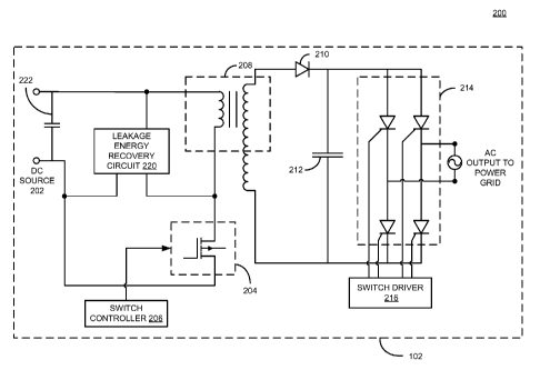
[0017] FIG. 2 is a schematic representation of an inverter 102 comprising a
leakage
energy recovery circuit 220 in accordance with one or more embodiments of the
present invention. The inverter 102 is coupled to a DC power source 202, such
as
the PV module 104, for providing DC voltage to the inverter 102. In addition
to the
leakage energy recovery circuit 220, the inverter 102 comprises a bypass
capacitor
222, a switch 204, a switch controller 206, a transformer 208, a diode 210, a
capacitor 212, a switch matrix 214, and a switch driver 216.
[0018] A primary winding of the transformer 208 and the switch 204 are coupled
in
series across the DC power source 202. A first and a second terminal of the
leakage
energy recovery circuit 220 are coupled to a first and a second terminal of
the
primary winding, respectively, to recover the leakage energy induced in the
transformer 208 in a manner that is described with respect to FIG. 3 below.
The
bypass capacitor 222 is coupled in parallel to the DC power source 202 and
additionally across the first and a third terminal of the leakage energy
recovery circuit
220. The bypass capacitor 222 stores the energy recovered by the leakage
energy
recovery circuit 220 for use by the inverter 102.
[0019] The switch controller 206 is coupled to a gate terminal of the switch
204 to
control the voltage applied to the primary winding of the transformer 208. The
diode
210 is coupled in series with a secondary winding of the transformer 208 for
rectifying the voltage across the secondary winding of the transformer 208.
The
capacitor 212 is coupled in parallel to the series combination of the diode
210 and
the secondary winding, i.e., the anode terminal of the diode 210 is connected
to a
first terminal of the secondary winding, the cathode terminal of the diode 210
is
connected to a first terminal of the capacitor 212, and a second terminal of
the
capacitor 212 is coupled to a second terminal of the secondary winding. The
capacitor 212 is further coupled across the switch matrix 214. The voltage
across
the capacitor 212 is applied to the switch matrix 214 which comprises, for
example,
four silicon controlled rectifiers arranged in an H-bridge pattern. In
alternative
4
CA 02717564 2010-09-02
WO 2009/111600 PCT/US2009/036101
embodiments, the switch matrix 214 may utilize one or more different switches,
such
as metal-oxide semiconductor field effect transistors (MOSFETs), bipolar
junction
transistors (BJTs), and the like. The switch driver 216 is coupled to the
switch matrix
214 for controlling the switching of the switch matrix 214.
[0020] The DC power source 202 applies a DC voltage to the primary winding of
the
transformer 208 in accordance with operation of the switch 204. In one
embodiment,
a MOSFET is used as the switch 204 due to its high switching speed and
efficiency.
However, in other embodiments, various other types of switches may be used.
The
gate terminal of the switch 204 is controlled by the switch controller 206
such that the
switch 204 is operated to apply a pulsed DC voltage to the primary winding of
the
transformer 208.
[0021] In response to the pulsed DC voltage in the primary winding of the
transformer 208, a pulsed DC voltage is produced as an output waveform in the
secondary winding of the transformer 208, where the pulsed DC voltage output
waveform is at a different voltage level than the pulsed DC voltage input
waveform.
Thus, the transformer 208 "steps up" the pulsed DC voltage applied to the
primary
winding.
[0022] The diode 210 and the capacitor 212 rectify the output voltage from the
transformer 208. The rectified output voltage is then applied to the H-bridge
switch
matrix 214. The switch matrix 214, as controlled by the switch driver 216,
selectively
applies current to the output terminals to form an output AC waveform that is
synchronized to the power grid, e.g., a frequency of 60 Hertz in some
embodiments.
[0023] FIG. 3 is a schematic representation of a leakage energy recovery
circuit 220
in accordance with one or more embodiments of the present invention. The
leakage
energy recovery circuit 220 is designed to recover and store energy from the
leakage
inductance of the transformer 208 and to feed such stored leakage energy back
to
the input of the inverter 102.
[0024] The leakage energy recovery circuit 220 comprises a clamp circuit 308
and a
charge pump 318. The series combination of the transformer 208 (primary
winding
CA 02717564 2010-09-02
WO 2009/111600 PCT/US2009/036101
shown) and the switch 204 are coupled to the clamp circuit 308 and the charge
pump 318 as described in detail below. The clamp circuit 308 acts as a leakage
energy storage circuit and stores leakage energy generated by the transformer
208,
while the charge pump 318 acts as a leakage energy transfer circuit by
monitoring
the amount of stored leakage energy and, at an appropriate time, applying the
accumulated stored leakage energy to the input of the transformer 208 (i.e.
the
bypass capacitor 222). Thus, the clamp circuit 308 and the charge pump 318
recover the leakage energy and re-circulate such leakage energy back to the
bypass
capacitor 222 for use by the inverter 102. In some embodiments, such as the
embodiments depicted in FIG. 3, the charge pump 318 is a "buck" converter
structure; in alternative embodiments, the charge pump 318 may be a step down
"flyback" structure.
[0025] The clamp circuit 308 includes a diode 310, a capacitor 312, and a pair
of
resistors 314, 316. The anode terminal of the diode 310 is coupled to the
second
terminal of the primary winding of the transformer 208, and the cathode
terminal of
the diode 310 is coupled to a first terminal of the capacitor 312 and a first
terminal of
the resistor 314. A second terminal of the resistor 314 is coupled in series
to a first
terminal of the resistor 316, and a second terminal of the resistor 316 is
coupled to a
second terminal of the capacitor 312; thus, the series combination of the
resistors
314 and 316 are coupled across the capacitor 312. Additionally, the second
terminal
of the capacitor 312 and the second terminal of the resistor 316 are coupled
to the
second terminal of switch 204.
[0026] In the clamp circuit 308, the leakage energy is coupled through the
diode 310
to the capacitor 312, which stores the leakage energy that has accumulated as
a
positive residual voltage across the switch 204. The leakage energy stored in
the
capacitor 312 is divided across the resistor pair 314, 316 to form a monitor
voltage,
Vmonitor, at the junction of the resistor pair 314, 316.
[0027] The charge pump 318 comprises a monostable circuit 320, a switch 322, a
diode 324, and an inductor 326. The switch 322 is coupled to the first
terminal of
the capacitor 312 and to the cathode terminal of the diode 324; the anode
terminal of
6
CA 02717564 2010-09-02
WO 2009/111600 PCT/US2009/036101
the diode 324 is coupled to the second terminal of the capacitor 312 and the
second
terminal of the switch 204. Additionally, the cathode terminal of the diode
324 is
coupled through the inductor 326 to the first terminal of the primary winding
of the
transformer 208. The inductor 326 acts as a low-pass filter to remove any
switch
transients created by the switch 322, while the diode 324 ensures the correct
biasing
across the switch 322 and enables the switch 322 to properly activate and
deactivate.
[0028] An output of the monostable circuit 320 is coupled to the gate terminal
of the
switch 322 for controlling the operation of the switch 322 (i.e. turning the
switch
on/off); thus, the monostable circuit 320 acts as a driving circuit for the
switch 322.
The monostable circuit 320 receives the monitor voltage, VmoNiToR, from the
clamp
circuit as a first input and a threshold voltage, VREF, as a second input.
When the
monitor voltage is less than the threshold voltage, the output of the
monostable
circuit 320 maintains the switch 322 in an off state and the leakage energy
charges
the capacitor 312. When the voltage across the capacitor 312 reaches a level
sufficient to cause the monitor voltage to exceed the threshold voltage, the
output of
the monostable circuit 320 drives the switch 322 in a conductive state. The
voltage
across the capacitor 312 is presented to the inductor 326, and the current
into the
inductor 326 rises until the monostable circuit 320 times out. The switch 322
then
switches off, and the diode 324 turns on to recycle the energy stored in the
inductor
326 into the bypass capacitor 222 until it is fully expensed. At that time,
the
monostable circuit 320 may be rerun as long as the voltage on the capacitor
312
results in a monitor voltage above the threshold voltage. The leakage energy
is thus
"fed-back" to the bypass capacitor 222 such that the leakage energy is
recovered for
use by the inverter 200.
[0029] The theoretical peak voltage present at the junction of the switch 204
and the
transformer 208 can be approximately described as V¨V/N+VouT/n, where VIN is
the
input voltage across the DC power source 202 and the bypass capacitor 222,
VouT is
the output voltage across the capacitor 22212, and n is the ratio of the
transformer
208. Any leakage energy surge will move the voltage over the theoretical peak
7
CA 02717564 2010-09-02
WO 2009/111600 PCT/US2009/036101
voltage value. In some embodiments, the optimum VREF for the leakage energy
recovery circuit 220 may be obtained utilizing the above formula (while
factoring in
the voltage divider of the resistor pair 314, 316) and with the addition of a
small
voltage margin.
[0030] FIG. 4 is a flow diagram of a method 400 for recovering leakage energy
in
accordance with one or more embodiments of the present invention. In some
embodiments, such as the embodiment described below, a DC-AC inverter converts
DC input power to AC output power. The DC-AC inverter comprises a step-up
transformer for converting the DC input power to a second DC power, resulting
in a
leakage inductance from the transformer.
[0031] The method 400 begins at step 402 and proceeds to step 404. At step
404,
leakage energy from the transformer leakage inductance is stored. In some
embodiments, the leakage energy is stored in a capacitor coupled across a
current
control switch that is coupled in series with the transformer, such as the
capacitor
312 within the clamp circuit 308 described above. At step 406, the amount of
leakage energy stored is monitored. In some embodiments, a monitor voltage is
obtained from a voltage divider coupled across the capacitor that stores the
leakage
energy. The monitor voltage provides an indication of the voltage across the
capacitor (i.e., the amount of leakage energy stored in the capacitor).
[0032] The method 400 proceeds to step 408, where the monitor voltage is
compared to a threshold voltage and a determination is made whether the
monitor
voltage exceeds the threshold voltage. An optimum threshold voltage may be
obtained in accordance with an input voltage of the transformer, an output
voltage of
the transformer, and a ratio of the transformer, where the voltage divider is
factored
in along with a small voltage margin, as previously described with respect to
Figure
3. If the monitor voltage does not exceed the threshold voltage, the method
400
returns to step 406. If the monitor voltage does exceed the threshold voltage,
sufficient leakage energy has been stored in the capacitor and the method 400
proceeds to step 410.
8
CA 02717564 2013-11-29
[0033] At step 410, the stored leakage energy is coupled to the input of the
DC-
AC inverter, for example to a bypass capacitor at the input of the DC-AC
inverter. In some embodiments, a monostable circuit drives a switch to close
(i.e., conduct) when the monitor voltage exceeds the threshold voltage and
thereby couples the stored leakage energy to the input of the DC-AC inverter.
The monostable circuit causes the switch to remain closed for a pre-determined
time, after which the switch opens and any leakage energy is again stored. The
method 400 then proceeds to step 412 where it ends.
[0034] Various embodiments as discussed herein, help in preventing the
wastage of the leakage energy in an inverter circuit by utilizing the leakage
energy. By utilizing the leakage energy, the embodiment of the present
invention
further helps in increasing the efficiency of the power inverter.
[0035] In the foregoing specification, one or more specific embodiments of the
present invention have been described. However, one of ordinary skill in the
art
will appreciate that various modifications and changes can be made without
departing from the scope of the present invention. Accordingly, the
specification
and figures are to be regarded in an illustrative rather than a restrictive
sense,
and all such modifications are intended to be included within the scope of
present invention. The benefits, advantages, solutions to problems, and any
element(s) that may cause any benefit, advantage, or solution to occur or
become more pronounced are not to be construed as a critical, required, or
essential features or elements as described herein.
9