Note : Les descriptions sont présentées dans la langue officielle dans laquelle elles ont été soumises.
CA 02817850 2013-06-18
POWER SOURCE
BACKGROUND
Technical Field
The invention relates to a power source, especially for use with a data bus in
public
transportation, wherein the power source has a first transistor and wherein,
in normal
operation of the power source, the current emitted by the first transistor is
determined by
a first resistor on the emitter of the first transistor.
Description of Related Art
In some areas of technology, power sources or current sinks with low precision
requirements are needed. One example of this is the supply of a data bus, e.g.
the
response bus of the IBIS and/or VDS vehicle bus, which is used in public
transportation.
The IBIS vehicle bus is used to control ticket validators, interior displays,
etc. in buses or
streetcars from a central control unit. The control unit assumes the function
of a master;
the individual users connected to the bus are slaves. By way of the call bus,
the master
sends a message to the individual slaves and the slaves report their status
back on the
response bus. The schematic structure of the bus is shown in Fig. 1. The
master has a
power source that outputs approx. 100 mA to the response bus. A slave that
wants to
transmit a message on the response bus, connects the line to ground according
to the
message to be sent using a transistor (a MOSFET in the figure) and thereby
creates a bit
pattern on the response bus. The voltage swing of the bit pattern typically
lies at 28 V. In
or at the master, the bit pattern is evaluated and the transmitted message is
extracted.
In this or similar applications, usually simply structured power sources are
used that
fulfill only low requirements for precision of the output current. Simple
circuits comprise
one or more bipolar transistors for driving the output current and few circuit
elements.
During the design of the circuit, among other things, attention must be paid
to the
maximum power loss in the transistor(s). To prevent overheating, frequently a
cooling
surface or a heat sink is used for a power transistor. However, because of
this the power
1
CA 2817850 2017-04-26
=
source becomes much more voluminous and ¨ with the use of heat sinks ¨ the
manufacturing
becomes more expensive and complicated. To avoid the use of heat sinks,
sometimes the current
supplied by the power source is distributed to several power transistors and a
cooling surface is
implemented on the circuit board. In this case, frequently SMD (surface mount
device) power
transistors are used. Still, a comparatively large cooling surface is
necessary, which involves a
not inconsiderable space requirement on the circuit board and thus costs. In
addition, it is
possible that a developer may take the circuit section over to a new circuit
board and not provide
adequately large cooling surfaces. This causes the risk of a component
overload.
Therefore, it may be desirable to design and further develop a power source of
the type named at
the beginning that can achieve safe operation of the power source
simultaneously with the
smallest possible space requirement. In this case, the power source can
especially be used with a
data bus in public transportation.
BRIEF SUMMARY
According to an aspect of the invention, there is provided a power source for
use with a data bus
in public transportation, the power source comprising: a first transistor
comprising an emitter, a
collector, and a base, wherein the first transistor emits an output current of
the power source; and
a temperature-dependent resistor thermally coupled with the first transistor,
wherein due to the
thermal coupling an increasing temperature of the first transistor results in
an increasing
temperature of the temperature-dependent resistor, wherein: during normal
operation of the
power source, the current emitted by the first transistor is determined by a
first resistor on the
emitter of the first transistor; the temperature-dependent resistor is in
circuit with the power
source in such a way that, during increasing temperature of the first
transistor due to current flow
through the first transistor, the temperature-dependent resistor influences a
voltage across the
first resistor and thereby produces a reduction in the output current of the
power source and a
limiting of the output current and thereby prevents an overload of the
transistor.
2
CA 2817850 2017-04-26
=
According to selected embodiments, the power source being discussed is
characterized in that a
temperature-dependent resistor is thermally coupled with the first transistor
and that the
temperature-dependent resistor is connected with the power source in such a
way
2a
CA 02817850 2013-06-18
that during increasing temperature of the first transistor, the temperature-
dependent
resistor influences the voltage and thereby produces a reduction in the output
current.
In a manner according to an embodiment of the invention, it is recognized at
first that in
many applications the power source cannot be continuously loaded in the limit
range.
Rather, a maximum power loss in the transistors frequently only occurs in the
case of a
fault. For example, in an IBIS vehicle bus in normal operation, the power
source can only
be loaded for approximately one-tenth to one-fifth of the time. Very high
loads occur
only in the case of a fault, e.g. a defect in a device that is connected or a
wiring fault.
Frequently, a short circuit on the line occurs then. Since data communication
is no longer
possible anyway in these cases, the power source does not have to supply the
current
continuously. However, to date, the power source has always been designed for
this case.
This means that, in the case of a short circuit, the power loss must be
discharged via
cooling surfaces or heat sinks.
During a short circuit, a power loss occurs that results as the product of the
maximum
supply voltage and the current supplied by the power source. For example, with
a voltage
supply of 32 V and a current of 100 mA, the power loss is 3.2 W.
However, during the design of the cooling capabilities for the circuit, it is
sufficient to
design the power source for normal operation and the average current that
flows. This
means that only the far lower current requirement of normal operation has to
be covered
and the power loss that then occurs has to be dissipated. For example, if the
named IBIS
vehicle bus is only loaded one-fifth of the time, a power loss of 28 V x 100
mA / 5 =
0.56 W occurs. This clearly lower power loss requires much smaller cooling
solutions, so
the circuit requires less surface area and in general does not need any heat
sinks.
To permit safe operation even in the case of a short circuit, a protective
measure may be
taken that intervenes in the case of a fault and prevents overheating of the
transistor. To
do this, a temperature-dependent resistor may be thermally coupled with the
power
source transistor. The temperature-dependent resistor is connected with the
power source
3
CA 02817850 2013-06-18
=
as a temperature sensor in such a way that the power output, and thus the
power loss, is
reduced.
Simple power sources with the use of a transistor have a resistor on the
transistor emitter,
which determines the maximum power output of the power source in wide ranges.
According to selected embodiments of the invention, the temperature-dependent
resistor
intervenes at exactly this point, namely in that it is connected in such a way
that with
increasing temperature of the transistor, the temperature-dependent resistor
influences the
voltage across the resistor on the transistor emitter. If the voltage drops,
only a lower
current can flow through the resistor and because of this, in turn the output
current
emitted by the power source is reduced. This means that if the circuit is
loaded with a
current that is too high, the transistor supplying the output current heats
up. Because of
the thermal coupling of the transistor with the temperature-dependent
resistor, the
temperature of the temperature-dependent resistor increases. In turn, this
acts on the
resistor and leads to a reduction in the output current of the power source.
In this way, a
type of feedback occurs that provides for prevention of an overload of the
transistor and
limiting of the current.
To simplify the further discussion, the transistor that drives the output
current of the
power source is designated as the first transistor. This does not mean that
the first
transistor always and exclusively comprises a single transistor. Rather,
several transistors
can be connected in parallel that mutually drive the output current. In such a
case, the
temperature-dependent resistor can still be thermally coupled with all the
transistors of
the driver stage. For example, it would be conceivable for four SMD power
transistors to
be soldered in a rectangle on the circuit board and the temperature-dependent
resister to
be mounted in the center.
In an exemplary design of the power source, the temperature-dependent resistor
is made
up of an NTC (negative temperature coefficient) resistor. These so-called
pyroelectric
conductors are better conductors with increasing temperature, i. e. the
resistance drops
with increasing temperature. NTCs with many different designs are known in
practice.
4
CA 02817850 2013-06-18
=
In an exemplary manner, the first transistor is a pnp transistor. The use of
pnp transistors
has the advantage that power sources can be constructed, in which an output
current can
be driven toward ground. This makes handling them easier, for example in bus
systems.
However, an npn transistor can also be used for the power source according to
the
invention. The mechanisms described apply analogously.
In an exemplary design of the power source, the temperature-dependent resistor
has two
connections, of which one is connected to the base of the first transistor and
the second of
which is connected to the end of the resistor on the first transistor emitter
turned away
from the transistor. The expression "end turned away from the transistor" is
understood in
electrical terms, i.e. the end of the resistor turned away from the transistor
is the end of
the resistor not connected to the transistor. Because of this type of wiring,
the
temperature-dependent resistor creates a type of bypass that reduces the
voltage over the
resistor on the transistor emitter and reduces the base-emitter voltage of the
transistor.
To improve the temperature stability of the power source, a reference voltage
can be
generated. With the wiring of the temperature-dependent resistor described
above, the
reference voltage can be applied across the serial connection of the resistor
on the emitter
of the first transistor and the emitter-base section of the first transistor.
Also, the
reference voltage is across the temperature-dependent resistor, which is
connected
parallel to the named series circuit.
In an exemplary manner, the reference voltage is generated with the use of one
diode or a
series connection of several diodes (i. e., two or more diodes). Thus a
reference voltage
occurs as a multiple of the knee voltage of the diodes used. For example, by
series
connection of two Si diodes, a reference voltage of 1.2 V can be generated.
For the sake
of completeness, reference is made to the fact that the reference voltage can
also be
generated in another way. In this way, for example, a reference voltage source
can be
used.
CA 02817850 2013-06-18
=
To improve the independence of the output current from the supply voltage, a
current
sink can be provided between base and collector of the first transistor. The
current sink
consists of a second transistor, on the emitter of which a resistor is
mounted. In parallel to
the base-emitter section of the second transistor and the resistor on the
emitter of the
second transistor, one or more diodes are connected for generating a reference
voltage.
The second transistor is designed as an npn transistor.
According to various embodiments, the base of the second transistor is
connected by way
of a resistor to the voltage source that supplies the power source with
energy.
For dissipating the power loss of the first transistor, this is connected
thermally to a
cooling surface. This cooling surface can be formed as a part of the circuit
board on
which the power source is designed. In this case, it makes sense to dimension
the cooling
surface in such a way that the current limiter, by means of the temperature-
dependent
resistor, does not respond in normal operation. This means that the cooling
surface and
the heat dissipation thereby provided are dimensioned such that the
temperature-
dependent resistor has only a slight, or no, influence on the output current
of the power
source. In normal operation, the power source is loaded as planned, i. e., no
short circuit
currents occur. The power limiter does not respond until more current is drawn
from the
power source than in normal operation.
A thermal coupling between the temperature-dependent resistor and the first
transistor
can be facilitated in that the temperature-dependent resistor and the
transistor are
mounted close to each other. The thermal coupling can be improved in that a
heat
conducting means is mounted between the first transistor and the temperature-
dependent
resistor. When the transistor is mounted on a cooling surface, the thermal
coupling can be
achieved in that the temperature-dependent resistor is thermally coupled with
the cooling
surface. If the cooling surface is formed of circuit board material, there is
a very good
thermal conductor, usually copper. Because of this, the temperature-dependent
resistor
reacts very quickly to heating of the first transistor and load peaks can be
intercepted very
quickly.
6
CA 02817850 2013-06-18
According to various embodiments, the power source provides a consumer, which,
on
average, stresses the power source less than 50 % of the time per time unit.
In an
exemplary manner, the consumer only stresses the power source less than 20 %
of the
time. In another exemplary manner, the power source is only stressed by the
consumer
less than 10 % of the time. Such a loading scenario occurs, for example, in
the IBIS bus
that has already been mentioned. Reference is made again to the fact that the
protective
circuit and the cooling surfaces are dimensioned with regard to the average
power loss of
the power source. However, a clearly higher current can be drawn in normal
operation.
The only prerequisite is that, on average, the power source is only loaded in
such a way
that the first transistor does not heat above the defined temperature. If the
temperature
increases above that, the protective circuit limits the output current.
BRIEF DESCRIPTION OF THE DRAWINGS
There are now various options for designing and further developing the
teaching of the
present invention in an advantageous manner. For this purpose, on one hand,
reference is
made to the claims and, on the other, to the following explanation of a
exemplary
embodiment of the invention with the use of the drawings. In connection with
the
explanation of the-exemplary embodiment of the invention with the use of the
drawings,
various designs and further developments of the teaching are explained. In the
drawings:
Fig. 1 shows the schematic structure of a response bus, in which a power
source
according to the invention can be used, and a typical voltage curve on the bus
master,
Fig. 2 shows an exemplary embodiment of the power source according to the
invention and
Fig. 3 shows the exemplary embodiment according to Fig. 2 with an exemplary
selection of components.
7
CA 02817850 2013-06-18
DETAILED DESCRIPTION OF VARIOUS EMBODIMENTS
Fig. 1 shows a schematic structure of a response bus and a typical voltage
curve during
data transmission in an IBIS vehicle bus. More details can be found in the
introductory
section of the description.
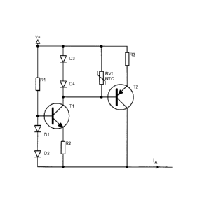
Fig. 2 shows an exemplary embodiment of a power source according to the
invention.
The power source is connected to a supply voltage V+ and supplies an output
current IA.
The output current IA essentially flows through a first resistor R3 that is
connected to the
voltage supply V+ and the emitter of a first bipolar transistor T2. The first
transistor T2 is
designed as a pnp transistor. A temperature-dependent resistor RV1 is
connected in
parallel to the first resistor R3 and the emitter-base section of the first
transistor T2. In
turn, a series circuit of two diodes D3 and D4 is connected to the temperature-
dependent
resistor. The base of the first transistor T2 is connected to the collector of
a second
bipolar transistor T1. The emitter of the second transistor T1 is connected to
a second
resistor R2. The other end of the second resistor R2 is connected to the
collector of the
first resistor T2 and the output of the power source. A series circuit of two
diodes D1 and
D2 is connected in parallel to the base-emitter section of the second
transistor T1 and the
second resistor R2. The base of the second bipolar transistor T1 is also
connected to a
third resistor R1, the other end of which is connected to the voltage source
V+.
As soon as the output of the circuit is stressed, i. e., a current IA will be
output by the
power source, the third resistor R1, creates a voltage drop of 0.6 V in each
of the diodes
D1 and D2. Thus a voltage drop of approx. 1.2 V occurs over the series circuit
of D1 and
D2. This voltage forms a reference voltage that is applied by way of the base-
emitter
section of the second transistor T1 and the second resistor R2. In this way, a
simple
current sink is formed by D1, D2, T1 and R2. For example, the current sink can
have an
output current of 2 mA.
In turn, the output current of the current sink creates a voltage drop of
approx. 1.2 V
together in the diodes D3 and D4. This reference voltage is applied, in turn,
by way of the
8
CA 02817850 2013-06-18
=
first resistor R3 and the emitter-base section of the first transistor T2 and
by way of the
temperature-dependent resistor RV1. Because of this voltage at the base of the
first
transistor T2, the circuit of T2 and T3 act as a power source. An example
output current
IA is 100 mA. The reference voltage formed by the diodes D3 and D4 provides
for a
certain compensation of the transistor temperature drift here. The circuit
made up of D1,
D2, T1 and R2 provides for independence from the supply voltage of the power
source
within certain limits.
The temperature-dependent RV1 and the remaining circuit are dimensioned in
such a way
that in normal operation of the power source, the temperature-dependent
resistor RV1 has
a negligible, or at least very little, influence on the behavior of the power
source. Here
normal operation defines the usual load on the power source as it has been
specified
during the dimensioning of the power source. For example, during use of the
power
source in connection with an IBIS vehicle bus, an average load over one-fifth
of the time
is assumed, as well as a supply voltage of 32 V, a voltage swing of 28 V in
the data signal
to be transferred and an output current from the power source of 100 mA.
In this case, the power source would be dimensioned for a power loss of 28 V x
100 mA /
= 0.56 W. Thus normal operation means that, as an average over time, the first
transistor T2 is not loaded with significantly more than the said 0.56 W.
If the power source is loaded with a definitely higher current, e.g. in the
case of a short
circuit, the temperature of the first transistor T2 increases more. Because of
the thermal
coupling of the variable resistor RV1 with the first transistor T2, the
temperature-
dependent resistor RV1 heats up. The temperature-dependent resistor RV1 is
designed as
NTC, so with increasing temperature its resistance drops. Because of this,
with increasing
temperature, increasingly more current flows through the temperature-dependent
resistor,
so the voltage difference between base and emitter of the first transistor T2
is no longer
determined from the series circuit of D3 and D4, but rather from the
temperature-
dependent resistor RV1. Starting at a specific temperature, this leads to a
case in which
the voltage drops over R3 and, because of this, the power output of the power
source is in
9
CA 02817850 2013-06-18
=
turn restricted. In turn, a restriction of the power output has a drop in the
power source
power loss as a consequence. In this way, the circuit itself stabilizes and
only a maximum
current is supplied, independently of the load. At the same time, in normal
operation of
the circuit, there is no influence on the output current. This means that the
power source
behaves like any power source without protective measures. If a short circuit
or an
excessively high load on the power source is no longer present, the first
transistor T2 and
the temperature-dependent resistor RV1 cool again and the power source returns
to
normal condition. In this way, a self-reset of the protective circuit is
achieved. The
cooling surface of the power source no longer has to be designed for the fault
case.
Rather, it is sufficient to select the cooling surface in such a way that in
normal operation,
the transistor does not heat above the response threshold of the protective
circuit.
A possible dimensioning of the power source is shown in Fig. 3. The first
resistor R3 is
formed by a 4.7 Q resistor. The second resistor R2 is 330 Q, the third
resistor R1 is
47 kO. The diodes D1 and D2 and/or D3 and D4 are formed by double diodes,
model
BAV99. An NTC from EPCOS, the B57371V2223+060 is used as temperature-
dependent resistor RV1. The first transistor 12 is formed by a BCP53-16. The
second
transistor T1 is fornied by a BC846. In this way, a power source that supplies
a current of
typically between approx. 90 mA and 110 mA in a temperature range from -40 to
+70 C
is produced. For example, in the case of a short circuit, if the NTC is heated
to 120 C, the
output current IA of the power source is already reduced to approx. 20 mA.
The circuit named as an example above, offers the considerable advantage that
clearly
lower cooling surfaces are necessary. Because of this, the entire power source
can be
built so that it is more economical and saves space. Heat sinks or several
power
transistors that would be necessary without the protective circuit according
to the
invention are not needed, which in turn has a positive effect on the costs of
the power
source. In the case of a short circuit, the power loss in the device is
clearly lower and the
entire device, i. e., the device in which the power source is installed,
definitely heats up
less.
CA 02817850 2013-06-18
=
With respect to additional advantageous designs of the device according to the
invention,
to prevent repetitions, reference is made to the general section of the
description, as well
as the claims included.
Finally, explicit reference is made to the fact that the exemplary embodiments
of the
device according to the invention described above are used only for
explanation of the
claimed teaching, but the teaching is not restricted to the exemplary
embodiments.
Reference number list
R1 Third resistor
R2 Second resistor
R3 First resistor
RV1 Temperature-dependent resistor
T1 Second transistor
T2 First transistor
D1 Diode
D2 Diode
D3 Diode
D4 Diode
V+ Supply voltage
IA Output voltage
11