Note : Les descriptions sont présentées dans la langue officielle dans laquelle elles ont été soumises.
CA 02889495 2015-04-23
WO 2014/070656
PCT/US2013/067068
Fourier Ptychographic Imaging Systems, Devices, and Methods
CROSS-REFERENCES TO RELATED APPLICATIONS
[0001] This is a non-provisional application of, and claims priority to, U.S.
Provisional
Patent Application No. 61/720,258 entitled "Breaking the Spatial Product
Barrier via Non-
Interferometric Aperture-Sythesizing Microscopy (NAM)," filed on Octobter 30,
2012 and to
U.S. Provisional Patent Application No. 61/847,472 entitled "Fourier
Ptychographic
Microscopy," filed on July 17, 2013. These provisional applications are hereby
incorporated
by reference in their entirety for all purposes.
BACKGROUND OF THE INVENTION
[0002] Embodiments of the present disclosure generally relate to wide field-of-
view, high-
resolution digital imaging techniques. More specifically, certain embodiments
relate to
Fourier ptychographic imaging (FPI) devices, systems and methods for wide-
field, high-
resolution imaging.
[0003] The throughput of a conventional imaging platform (e.g., microscope) is
generally
limited by the space-bandwidth product defined by its optical system. The
space-bandwidth
product refers to the number of degrees of freedom (e.g., number of resolvable
pixels) that
the optical system can extract from an optical signal, as discussed in
Lohmann, A. W.,
Dorsch, R. G., Mendlovic, D., Zalevsky, Z. & Ferreira, C., "Space¨bandwidth
product of
optical signals and systems," J. Opt. Soc. Am. A 13, pages 470-473 (1996),
which is hereby
incorporated by reference in its entirety. A conventional microscope typically
operates with a
space-bandwidth product on the order of 10 megapixels, regardless of the
magnification
factor or numerical aperture (NA) of its objective lens. For example, a
conventional
microscope with a x20, 0.40 NA objective lens has a resolution of 0.8mm and a
field-of-view
of 1.1mm in diameter, which corresponds to a space-bandwidth product of about
7
megapixels. Prior attempts to increase space-bandwidth product of conventional
microscopes
have been confounded by the scale-dependent geometric aberrations of their
objective lenses,
which results in a compromise between image resolution and field-of-view.
Increasing the
space-bandwidth product of conventional imaging platforms may be limited by:
1) scale-
dependent geometric aberrations of its optical system, 2) constraints of the
fixed mechanical
length of the relay optics and the fixed objective parfocal length, and/or 3)
availability of
gigapixel digital recording devices.
CA 02889495 2015-04-23
WO 2014/070656
PCT/US2013/067068
[0004] Some attempts to increase the spatial-bandwidth product using
interferometric
synthetic aperture techniques are described in Di, J. et at., "High resolution
digital
holographic microscopy with a wide field of view based on a synthetic aperture
technique
and use of linear CCD scanning," Appl. Opt. 47, pp. 5654-5659 (2008); Hillman,
T. R.,
Gutzler, T., Alexandrov, S. A., and Sampson, D. D., "High-resolution, wide-
field object
reconstruction with synthetic aperture Fourier holographic optical
microscopy," Opt. Express
17, pp. 7873-7892 (2009); Granero, L., Mid), V., Zalevsky, Z., and Garcia, J.,
"Synthetic
aperture superresolved microscopy in digital lensless Fourier holography by
time and angular
multiplexing of the object information," Appl. Opt. 49, pp. 845-857 (2010);
Kim, M. et al.,
"High-speed synthetic aperture microscopy for live cell imaging," Opt. Lett.
36, pp. 148-150
(2011); Turpin, T., Gesell, L., Lapides, J., and Price, C., "Theory of the
synthetic aperture
microscope," pp. 230-240; Schwarz, C. J., Kuznetsova, Y., and Brueck, S.,
"Imaging
interferometric microscopy," Optics letters 28, pp. 1424-1426 (2003); Feng,
P., Wen, X., and
Lu, R., "Long-working-distance synthetic aperture Fresnel off-axis digital
holography,"
Optics Express 17, pp. 5473-5480 (2009); Mico, V., Zalevsky, Z., Garcia-
Martinez, P., and
Garcia, J., "Synthetic aperture superresolution with multiple off-axis
holograms," JOSA A 23,
pp.3162-3170 (2006); Yuan, C., Zhai, H., and Liu, H., "Angular multiplexing in
pulsed
digital holography for aperture synthesis," Optics Letters 33, pp. 2356-2358
(2008); Mico,
V., Zalevsky, Z., and Garcia, J., "Synthetic aperture microscopy using off-
axis illumination
and polarization coding," Optics Communications, pp. 276, 209-217 (2007);
Alexandrov, S.,
and Sampson, D., "Spatial information transmission beyond a system's
diffraction limit using
optical spectral encoding of the spatial frequency," Journal of Optics A: Pure
and Applied
Optics 10, 025304 (2008); Tippie, A.E., Kumar, A., and Fienup, J.R., "High-
resolution
synthetic-aperture digital holography with digital phase and pupil
correction," Opt. Express
19, pp. 12027-12038 (2011); Gutzler, T., Hillman, T.R., Alexandrov, S.A., and
Sampson,
D.D., "Coherent aperture-synthesis, wide-field, high-resolution holographic
microscopy of
biological tissue," Opt. Lett. 35, pp. 1136-1138 (2010); and Alexandrov, S.A.,
Hillman, T.R.,
Gutzler, T., and Sampson, D.D., "Synthetic aperture Fourier holographic
optical
microscopy," Phil. Trans. R. Soc. Lond. A 339, pp. 521-553 (1992), which are
hereby
incorporated by reference in their entirety. Most of these attempts use setups
that record both
intensity and phase information using interferometric holography approaches,
such as off-line
holography and phase-shifting holography. The recorded data is then
synthesized in the
Fourier domain in a deterministic manner.
2
CA 02889495 2015-04-23
WO 2014/070656
PCT/US2013/067068
[0005] These previous attempts to increase spatial-bandwidth product using
interferometric
synthetic aperture techniques have limitations. For example, interferometric
holography
recordings typically used in these techniques require highly-coherent light
sources. As such,
the reconstructed images tend to suffer from various coherent noise sources,
such as speckle
noise, fixed pattern noise (induced by diffraction from dust particles and
other optical
imperfections in the beam path), and multiple interferences between different
optical
interfaces. The image quality is, therefore, not comparable to that of a
conventional
microscope. On the other hand, the use of an off-axis holography approach
sacrifices useful
spatial-bandwidth product (i.e., the total pixel number) of the image sensor,
as can be found
in Schnars,U. and Jiiptner,W.P.O., "Digital recording and numerical
reconstruction of
holograms," Measurement Science and Technology, 13, R85 (2002), which is
hereby
incorporated by reference in its entirety. Another limitation is that
interferometric imaging
may be subjected to uncontrollable phase fluctuations between different
measurements.
Hence, a priori and accurate knowledge of the specimen location may be needed
for setting a
reference point in the image recovery process (also known as phase referring).
Another
limitation is that previously reported attempts require mechanical scanning,
either for rotating
the sample or for changing the illumination angle. Therefore, precise optical
alignments,
mechanical control at the sub-micron level, and associated maintenances are
needed for these
systems. In terms of the spatial-bandwidth product, these systems present no
advantage as
compared to a conventional microscope with sample scanning and image
stitching. Another
limitation is that previous interferometric synthetic aperture techniques are
difficult to
incorporate into most existing microscope platforms without substantial
modifications.
Furthermore, color imaging capability has not been demonstrated on these
platforms. Color
imaging capability has proven pivotal in pathology and histology applications.
[0006] In microscopy, a large spatial-bandwidth product is highly desirable
for biomedical
applications such as digital pathology, haematology, phytotomy,
immunohistochemistry, and
neuroanatomy. A strong need in biomedicine and neuroscience to digitally image
large
numbers of histology slides for analysis has prompted the development of
sophisticated
mechanical scanning microscope systems and lensless microscopy set-ups.
Typically, these
systems increase their spatial-bandwidth product using complex mechanical
means that have
high precision and accurate components to control actuation, optical alignment
and motion
tracking. These complex components can be expensive to fabricate and difficult
to use.
3
CA 02889495 2015-04-23
WO 2014/070656
PCT/US2013/067068
[0007] Previous lensless microscopy methods such as digital in-line holography
and
contact-imaging microscopy also present certain drawbacks. For example,
conventional
digital in-line holography does not work well for contiguous samples and
contact-imaging
microscopy requires a sample to be in close proximity to the sensor. Examples
of digital in-
line holography devices can be found in Denis, L., Lorenz, D., Thiebaut, E.,
Fournier, C. and
Trede, D., "Inline hologram reconstruction with sparsity constraints," Opt.
Lett. 34, pp. 3475-
3477 (2009); Xu, W., Jericho, M., Meinertzhagen, I., and Kreuzer, H., "Digital
in-line
holography for biological applications," Proc. Natl Acad. Sci. USA 98, pp.
11301-11305
(2001); and Greenbaum, A. et al., "Increased space¨bandwidth product in pixel
super-
resolved lensfree on-chip microscopy," Sci. Rep. 3, page 1717 (2013), which
are hereby
incorporated by reference in their entirety. Examples of contact-imaging
microscopy can be
found in Zheng, G., Lee, S. A., Antebi, Y., Elowitz, M. B. and Yang, C., "The
ePetri dish, an
on-chip cell imaging platform based on subpixel perspective sweeping
microscopy (SPSM),"
Proc. Natl Acad. Sci. USA 108, pp. 16889-16894 (2011); and Zheng, G., Lee, S.
A., Yang, S.
& Yang, C., "Sub-pixel resolving optofluidic microscope for on-chip cell
imaging," Lab Chip
10, pages 3125-3129 (2010), which are hereby incorporated by reference in
their entirety.
BRIEF SUMMARY OF THE INVENTION
[0008] Embodiments of the present disclosure provide Fourier ptychographic
imaging
(FPI) methods, devices, and systems for wide-field, high-resolution imaging as
used in
applications such as, for example, digital pathology, haematology,
semiconductor wafer
inspection, and X-ray and electron imaging. An example of an FPI device is a
Fourier
ptychographic microscope (FPM), which may also be referred to as employing non-
interferometric aperture-synthesizing microscopy (NAM).
[0009] In some embodiments, an FPI system includes a variable illuminator,
optical
element, radiation detector, and a processor. The variable illuminator
illuminates a specimen
from a plurality of N different incidence angles at different sample times.
The optical
element filters light issuing from the specimen. The radiation detector
captures a plurality of
variably-illuminated (perspective) low-resolution intensity images. The
processor iteratively
stitches together the variably-illuminated, low-resolution images of
overlapping regions in
Fourier space to recover a wide-field, high-resolution image. In certain
embodiments, the
FPI device may also correct for aberrations and digitally refocus the complex
high-resolution
4
CA 02889495 2015-04-23
WO 2014/070656
PCT/US2013/067068
image, which can digitally extend the depth of focus of the FPI system beyond
the physical
limitations of its optical element.
[0010] One embodiment provides a Fourier ptychographic imaging device
comprising a
variable illuminator for providing illumination to a specimen from a plurality
of incidence
angles, an optical element for filtering illumination issuing from the
specimen, and a detector
for acquiring a plurality of variably-illuminated, low-resolution intensity
images of the
specimen based on light filtered by the optical element. The Fourier
ptychographic imaging
device also comprises a processor for computationally reconstructing a high-
resolution image
of the specimen by iteratively updating overlapping regions in Fourier space
with the
variably-illuminated, low-resolution intensity images. In one case, the
variable illuminator is
a two-dimensional matrix of light elements (e.g., light-emitting diodes), each
light element
providing illumination from one of the plurality of incidence angles.
[0011] Another embodiment provides a method of Fourier ptychographic imaging.
The
method illuminates a specimen being imaged from a plurality of incidence
angles using a
variable illuminator and filters light issuing from (e.g., scattered by) the
specimen using an
optical element. The method also captures a plurality of variably-illuminated,
low-resolution
intensity images of the specimen using a detector. Also, the method
computationally
reconstructs a high-resolution image of the specimen by iteratively updating
overlapping
regions of variably-illuminated, low-resolution intensity images in Fourier
space. In one case,
the method initializes a current high-resolution image in Fourier space,
filters an filtering an
overlapping region of the current high-resolution image in Fourier space to
generate a low-
resolution image for an incidence angle of the plurality of incidence angles,
replaces the
intensity of the low-resolution image with an intensity measurement, and
updates the
overlapping region in Fourier space with the low-resolution image with
measured intensity.
In this case, the filtering, replacing, and updating steps may be performed
for the plurality of
incidence angles. In another case, the method divides each variably-
illuminated, low-
resolution intensity image into a plurality of variably-illuminated, low-
resolution intensity tile
images, recovers a high-resolution image for each tile by iteratively updating
overlapping
regions of variably-illuminated, low-resolution intensity tile images in
Fourier space, and
combines the high resolution images of the tiles to generate the high-
resolution image of the
specimen.
5
CA 02889495 2015-04-23
WO 2014/070656
PCT/US2013/067068
[0012] Another embodiment provides a method of Fourier ptychographic imaging
that
receives a plurality of variably-illuminated, low-resolution intensity images
of a specimen
and computationally reconstructs a high-resolution image of the specimen by
iteratively
updating overlapping regions of variably-illuminated, low-resolution intensity
images in
Fourier space. In one case, the method divides each variably-illuminated, low-
resolution
intensity image into a plurality of variably-illuminated, low-resolution
intensity tile images,
recovers a high-resolution image for each tile by iteratively updating
overlapping regions of
variably-illuminated, low-resolution intensity tile images in Fourier space,
and combines the
high-resolution images of the tiles. In another case, the method initializes a
current high-
resolution image in Fourier space, filters an overlapping region of the
current high-resolution
image in Fourier space to generate a low-resolution image for an incidence
angle of the
plurality of incidence angles, replaces intensity of the low-resolution image
with an intensity
measurement, and updates the overlapping region in Fourier space with the low-
resolution
image with measured intensity. In this case, the filtering, replacing, and
updating steps may
be performed for the plurality of incidence angles.
[0013] Certain embodiments provide FPI systems and devices for X-ray imaging
and
methods of using FPI systems and devices for X-ray imaging. One embodiment
provides a
Fourier ptychographic X-ray imaging device that comprises an assembly for
capturing a
plurality of variably-illuminated, low-resolution intensity X-ray images of a
specimen. The
Fourier ptychographic X-ray imaging device further comprise a processor for
computationally reconstructing a high-resolution X-ray image of the specimen
by iteratively
updating overlapping regions in Fourier space with the variably-illuminated,
low-resolution
intensity X-ray images. In one case, the assembly comprises an X-ray optical
element and an
X-ray radiation detector, which are rigidly movable together with the
specimen. The X-ray
optical element is between the specimen and the X-ray radiation detector. The
X-ray
radiation detector captures the plurality of low-resolution intensity images
of the specimen
based on X-ray radiation projected by the X-ray optical element. In this case,
the Fourier
ptychographic X-ray imaging device may also comprise a mechanism for moving
the
assembly to direct X-ray radiation from a stationary X-ray radiation source to
the specimen
from the plurality of incidence angles.
[0014] Another embodiment provides a method of Fourier ptychographic X-ray
imaging.
This method acquires a plurality of variably-illuminated, low-resolution
intensity X-ray
images of a specimen based on a plurality of incidence angles and
computationally
6
CA 02889495 2015-04-23
WO 2014/070656
PCT/US2013/067068
reconstructs a high-resolution X-ray image of the specimen by iteratively
updating
overlapping regions of variably-illuminated, low-resolution intensity X-ray
images in Fourier
space. In one case, the method further comprises moving an assembly comprising
an X-ray
optical element and an X-ray radiation detector to provide X-ray radiation to
the specimen
from a plurality of incidence angles. In this case, the method further
comprises filtering the
X-ray radiation issuing from the specimen using the X-ray optical element and
capturing with
the X-ray radiation detector the plurality of variably-illuminated, low-
resolution intensity X-
ray images based on X-ray radiation projected by the X-ray optical element.
BRIEF DESCRIPTION OF THE DRAWINGS
[0015] FIG. lA is a schematic diagram of components of an FPI system,
according to
embodiments of the invention.
[0016] FIG. 1B is a schematic diagram of a side view of some components of the
FPI
device of FIG. 1A.
[0017] FIG. 2A is a schematic diagram of a FPI device comprising a variable
illuminator in
the form of a two-dimensional (10 x 10) matrix of 100 light elements,
according to an
embodiment of the invention.
[0018] FIG. 2B is a photograph of an FPI system with components in modular
form,
according to embodiments of the invention.
[0019] FIG.2C is a photograph of one of the light elements of the variable
illuminator the
FPI device of FIG. 2B.
[0020] FIG. 3 is a schematic diagram of a side view of components of an FPI
device,
according to embodiments of the invention.
[0021] FIG. 4A is a schematic diagram of a side view of components of an FPI
device,
according to embodiments of the invention.
[0022] FIG. 4B is a schematic diagram of a side view of components of an FPI
device,
according to embodiments of the invention.
[0023] FIG. 5A includes a schematic representation of the measurement process
(middle)
and a recovery process (right-hand side) of an FPI method, according to
embodiments of the
invention.
7
CA 02889495 2015-04-23
WO 2014/070656
PCT/US2013/067068
[0024] FIGS. 5B(1), 5B(2), 5B(3), 5B(4), 5B(5), 5B(6), 5B(7), 5B(8), and 5B(9)
are nine
low-resolution measurements acquired by the FPI method introduced in FIG. 5A.
[0025] FIG. 5B(12) are regions updated in Fourier space associated with low-
resolution
measurements of FIGS. 5B(1), 5B(2), 5B(3), 5B(4), 5B(5), 5B(6), 5B(7), 5B(8),
and 5B(9).
[0026] FIGS. 5B(10) and 5B(11) are the recovered high-resolution intensity and
phase
images resulting from the updating of FIG. 5B(12).
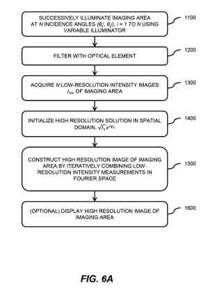
[0027] FIG. 6A is a flowchart of an FPI method performed by an FPI system,
according to
embodiments of the invention.
[0028] FIG. 6B is a flowchart of sub-steps of step 1500 of FIG. 6A, according
to an
embodiment of the invention.
[0029] FIGS. 6C and 6D are schematic diagrams of components of an FPI device
with
light elements in the form of an LED matrix, according to embodiments of the
invention.
[0030] FIG. 6E is an illustration of steps of the FPI method described with
reference to
FIGS. 6A and 6B.
[0031] FIG. 6F is another illustration of steps of the FPI method described
with reference
to FIGS. 6A and 6B.
[0032] FIGS. 7A(1), 7A(2), 7A(3), 7A(4), and 7A(5) are images resulting from
performing
the FPI method of FIGS. 6A and 6B.
[0033] FIGS. 7B(1), 7B(2), 7B(3), 7B(4), 7B(5) and 7B(6) are images resulting
from
performing the FPI method of FIGS. 6A and 6B with different N numbers (N= 5,
64, and
137) of incidence angles.
[0034] FIG. 8A is a flowchart of an FPI method with tile imaging, according to
an
embodiment of the invention.
[0035] FIG. 8B are images resulting from preforming an FPI method with tile
imaging
using image blending, according to an embodiment of the invention.
[0036] FIG. 9A is an FPI method with digital wavefront correction, according
to an
embodiment of the invention.
[0037] FIG. 9B is a schematic diagram of an FPI device implementing an FPI
method with
digital wavefront correction, according to an embodiment of the invention.
8
CA 02889495 2015-04-23
WO 2014/070656
PCT/US2013/067068
[0038] FIG. 10A are images from a numerical simulation of an FPI system 10
using an FPI
method with and without digital refocusing for comparison, according to an
embodiment of
the invention.
[0039] FIGS. 10B(1)-(16) show experimental results from performing an FPI
method with
digital refocusing, according to an embodiment of the invention, using the FPI
device 100(a)
shown in FIG. 2B.
[0040] FIG. 10B(1) is a schematic diagram of the experimental setup of an FPI
device
performing an FPI method with digital refocusing, according to an embodiment.
[0041] FIGS. 10B(2)-(16) are images of the experimental results from
performing the FPI
method with digital refocusing according the experimental setup in FIG.
10B(1).
[0042] FIGS. 10C(1)-(7) include more detailed results from the experiment
described with
respect to FIGS. 10B(1)-10B(16).
[0043] FIGS. 10D(1)-(3) are images of experimental results from performing the
FPI
method with and without digital refocusing for comparison, according to an
embodiment of
the invention.
[0044] FIGS. 10E(1), 10E(2), 10E(3), 10E(4), 10E(5), 10E(6), 10E(7), and
10E(8)
provides exemplary results from using an FPI system to perform an FPI method
with digital
refocusing, according to an embodiment of the invention, that corrects for
chromatic
aberration in a blood smear and in a pathology slide.
[0045] FIGS. 10F(1),10F(2),10F(3), 10F(4), 10F(5), 10F(6), and 10F(7) include
experimental results from using an FPI system to perform an FPI method with
digital
autofocusing, according to an embodiment of the invention.
[0046] FIG. 11A(1) is a photograph illustrating the fields-of-view of a
pathology slide for
both 2X and 20X objective lenses of conventional microscopes, for comparison.
[0047] FIGS. 11A(2) and 11A(3) are images illustrating the numerical aperture
for the 2X
objective lens in a conventional microscope.
[0048] FIGS. 11A(4) and 11A(5) are images illustrating the numerical aperture
for the 20X
objective lens in a conventional microscope.
9
CA 02889495 2015-04-23
WO 2014/070656
PCT/US2013/067068
[0049] FIGS. 11A(6) and FIG. 11A(7) are color images showing the field-of-view
and
corresponding maximum NA of an FPI system, according to an embodiment of the
invention.
[0050] FIGS. 11B(1)-(21) are images resulting from using a color imaging FPI
system,
according to an embodiment of the invention.
[0051] FIGS. 11C(1), 11C(2), 11C(3), 11C(4), 11C(5) and 11C(6) are images
showing a
comparison of image quality between the color imaging FPI system and different
objective
lenses, according to embodiments of the invention.
[0052] FIGS. 11D(1)-(10) are phase and color images from using an FPI method
with the
color imaging FPI system 10 both a pathology slide and blood smear, according
to an
embodiment of the invention.
[0053] FIG. 12 is a block diagram of subsystems that may be present in a FPI
system 10,
according to embodiments.
DETAILED DESCRIPTION OF THE INVENTION
[0054] Embodiments of the present invention will be described below with
reference to the
accompanying drawings. Although embodiments of FPI systems, devices, and
methods may
be described herein with respect to illumination with visible light radiation,
these FPI
systems, devices, and methods may also be used with other forms of radiation
such as, for
example, acoustic waves, Terahertz waves, microwaves, and X-rays.
[0055] Some embodiments include an FPI system comprising a variable
illuminator, optical
element, radiation detector, and a processor. The variable illuminator
successively
illuminates a specimen being imaged with plane waves at a plurality of N
different incidence
angles. The optical element filters light issuing from the specimen. The
optical element may
be, for example, an objective lens that accepts light issuing from the
specimen based on its
numerical aperture. In some cases, the optical element may be a low numerical
aperture
objective lens that provides a corresponding narrow acceptance angle and
increased depth of
field. The radiation detector detects light filtered by the optical element
and captures a
plurality of N low-resolution intensity images corresponding to the N
different incidence
angles. The processor iteratively stitches together overlapping low-resolution
intensity
images in Fourier space to recover a wide-field, high-resolution image of the
specimen. In
certain embodiments, the FPI device can also digitally refocus the complex
high-resolution
image to accommodate for defocus and aberrations in its optical element, which
may digitally
CA 02889495 2015-04-23
WO 2014/070656
PCT/US2013/067068
extend the depth of focus of the FPI system beyond the physical limitations of
its optical
element.
[0056] In certain aspects, an FPI method, performed by the FPI system,
comprises a
measurement process, a recovery process, and an optional display process.
During the
measurement process, the specimen is successively illuminated from the
plurality of N
incidence angles and corresponding low-resolution intensity images are
acquired. During the
recovery process, one or more high-resolution, wide field-of-view images are
recovered
based on the low-resolution intensity measurements. During the optional
display process, the
recovered images and other output is provided to the user of the FPI system on
a display.
I. INTRODUCTION TO FPI SYSTEMS AND DEVICES
[0057] Although embodiments of FPI devices and systems are described herein
with
respect to visible light radiation (illumination), other forms of radiation
(e.g., X-ray) may be
used in certain cases.
[0058] FIG. lA is a schematic diagram of components of an FPI system 10,
according to
embodiments of the invention. The FPI system 10 comprises an FPI device 100
and a
computing device 200 in electronic communication with FPI device 100. In
certain
embodiments, such as the one illustrated in FIG. 1A, a specimen 20 is provided
to the FPI
device 100 for imaging. The FPI device 100 comprises a variable illuminator
110 for
providing variable illumination to the specimen 20, an optical element 130 for
filtering
illumination issuing from the specimen 20, and a radiation detector 140 for
detecting intensity
of illumination received. The computing device 200 comprises a processor 210
(e.g., a
microprocessor), a computer readable medium (CRM) 220, and a display 230.
[0059] During a measurement process, the variable illuminator 110 provides
illumination
from a plurality of N incidence angles, (0,', i=1 to N to the specimen 20.
Illumination
from variable illuminator 110 may be altered (e.g., blocked, reduced
intensity, modified
wavelength/phase, modified polarization, etc.) by specimen 20 provided to the
FPI device
100. The optical element can receive light from the variable illuminator, for
example, as
issuing from the specimen 20 and can filter the light it receives. For
example, the optical
element 130 may be in the form of an objective lens, which accepts light
within its
acceptance angle to act as a filter. In some cases, the optical element 130
may be an
objective lens having a low numerical aperture (e.g., NA of about 0.08) to
provide a
corresponding narrow acceptance angle and allow for an increased depth of
field. The
11
CA 02889495 2015-04-23
WO 2014/070656
PCT/US2013/067068
radiation detector 140 can receive the filtered light from the optical element
130 and can
record an intensity distribution at the radiation detector 140 at N sample
times, t,=1 to N, to
capture a plurality of N low-resolution two-dimensional intensity images of
the specimen
area.
[0060] In FIG. 1A, the processor 210 is in electronic communication with
radiation
detector 140 to receive signal(s) with the image data corresponding to N low-
resolution
intensity images of the specimen area, which may include an image of at least
a portion of the
specimen 20. During a recovery process, the processor 210 can iteratively
"stitch" together
low-resolution intensity images in Fourier space to recover a wide-field, high-
resolution
image. In certain embodiments, the processor 210 can also digitally refocus
the high-
resolution image to accommodate for any defocus of the specimen and/or
chromatic
aberrations in its optical element 130. This capability can digitally extend
the depth of focus
of the FPI system 10 beyond the physical limitations of optical element 130.
[0061] Processor 210 is in electronic communication with CRM 220 (e.g.,
memory) to be
able to transmit signals with image data in order to store to and retrieve
image data from the
CRM 220. Processor 210 is shown in electronic communication with display 230
to be able
to send image data and instructions to display the wide-field, high-resolution
image of the
specimen area and other output, for example, to a user of the FPI system 10.
As shown by a
dotted line, variable illuminator 110 may optionally be in electronic
communication with
processor 210 to send instructions for controlling variable illuminator 110.
As used herein,
electronic communication between components of FPI system 10 may be in wired
or wireless
form.
[0062] FIG. 1B is a schematic diagram of a side view of some components of the
FPI
device 100 of FIG. 1A. In FIG. 1135 the FPI device 100 comprises a variable
illuminator 110
having an illuminator surface 1115 an optical element 130, and a radiation
detector 140
having a sensing surface 142. Although radiation detector 140 is shown at a
distance away
from optical element 130, radiation detector 140 may optionally be located at
the optical
element 130.
[0063] In certain embodiments, the FPI device comprises an in-focus plane 122
and a
sample plane 124. An in-focus plane 122 can refer to the focal plane of the
optical element
of the corresponding FPI device. The FPI device includes an x-axis and a y-
axis at the in-
focus plane 122, and a z-axis orthogonal to the in-focus plane 122. The in-
focus plane is
12
CA 02889495 2015-04-23
WO 2014/070656
PCT/US2013/067068
defined at an x-y plane at z = 0. A sample plane 124 can refer to the plane at
which the FPI
device may computationally reconstruct the high-resolution wide field-of-view
image. The
FPI device captures the low-resolution images at the in-focus plane 122.
Generally, the
sample plane 124 is parallel to the in-focus plane 122. In some embodiments,
the sample
plane 124 may be coincident to the in-focus plane 122. In an autofocus
embodiment, the FPI
system 10 may perform an FPI method that can determine the location of the
specimen 20 to
locate the sample plane 124 at the specimen 20 in order to focus the high-
resolution wide
field-of-view image at the specimen 20.
[0064] In FIG. 1B, the FPI device 100 includes an in-focus plane 122 at z = 0
and a sample
plane at z = zo. The FPI device 100 includes an x-axis and ay-axis (not shown)
in the in-
focus plane 122, and a z-axis orthogonal to the in-focus plane 122. The FPI
device 100 also
includes a distance d between the variable illuminator 110 and the sample
plane 124. In the
illustrated example, specimen 20 has been located at a specimen surface 126
for imaging. In
other embodiments, specimen 20 may be in other locations for imaging purposes.
[0065] In FIG. 1B, the FPI device 100 is shown at a particular sample time, tõ
in the
measurement process. At sample time, tõ variable illuminator 110 provides
incident
illumination at a wavevector associated with an incidence angle of A',
Oy) at the
sample plane 124. Since the illustration is a side view in an x-z plane, only
the x-component
Ox.' of the incidence angle is shown.
[0066] In FIG. 1B, the optical element 130 receives and filters light issuing
from specimen
20. Light filtered by the optical element 130 is received at the sensing
surface 142 of the
radiation detector 140. The radiation detector 140 senses the intensity
distribution of the
filtered light and captures a low-resolution intensity image of the specimen
area. Although
FPI device 100 is shown at a sample time, tõ the FPI device 100 can operate
during a
plurality of N sample times, t,itoN to capture N low-resolution two-
dimensional intensity
images associated with N incidence angles A', i=1 to N.
[0067] A variable illuminator can refer to a device that provides incident
radiation from a
plurality of N different incidence angles A',
i =1 to N, in succession. Suitable values of
N may range from 2 to 1000. In most embodiments, the variable illuminator
includes a light
element of one or more radiation sources providing illumination at a
particular sample time.
In most cases, each light element is approximated as providing plane wave
illumination to the
specimen 20 from a single incidence angle. For example, the incidence angle
Ox.' at reference
13
CA 02889495 2015-04-23
WO 2014/070656
PCT/US2013/067068
point, P, in FIG. 2A may be the angle between a normal and a line between
point, P and the
illuminated light element 112, which is based on a distance d between the
variable
illuminator and the sample plane 124.
[0068] Although the radiation source or radiation sources are usually coherent
radiation
sources, incoherent radiation source(s) may also be used and computational
corrections may
be applied. In embodiments that use visible light radiation, each radiation
source is a visible
light source. Some examples of a source of visible light include an LCD pixel
and a pixel of
an LED display. In embodiments that use other forms of radiation, other
sources of radiation
may be used. For example, in embodiments that use X-ray radiation, the
radiation source
may comprise an X-ray tube and a metal target. As another example, in
embodiments that
use microwave radiation, the radiation source may comprise a vacuum tube. As
another
example, in embodiments that use acoustic radiation, the radiation source may
be an acoustic
actuator. As another example, in embodiments that use Terahertz radiation, the
radiation
source may be a Gunn diode. One skilled in the art would contemplate other
sources of
radiation.
[0069] In many embodiments, the properties (e.g., wavelength(s),
frequency(ies), phase,
amplitude, polarity, etc.) of the radiation provided by the variable
illuminator at different
incidence angles, A', i=1 to N, is approximately uniform. In other
embodiments, the
properties may vary at the different incidence angles, for example, by
providing n different
wavelengths 21,...,2n during the measurement process. In one embodiment, the
variable
illuminator 110 may provide RGB illumination of three wavelengths 2i, 22, and
23
corresponding to red, green, blue colors, respectively. In embodiments that
use Terahertz
radiation, the frequencies of the radiation provided by the variable
illuminator 110 may be in
the range of 0.3 to 3 THz. In embodiments that use microwave radiation, the
frequencies of
the radiation provided by the variable illuminator may be in the range of 100
MHz to 300
GHz. In embodiments that use X-ray radiation, the wavelengths of the radiation
provided by
the variable illuminator may be in the range of 0.01m to lOnm. In embodiments
that use
acoustic radiation, the frequencies of the radiation provided by the variable
illuminator may
be in the range of 10Hz to 100MHz.
[0070] In some embodiments, the variable illuminator comprises a plurality ofN
stationary
light elements at different spatial locations (e.g., variable illuminator
110(a) in FIG. 2A).
These N stationary light elements illuminate at N sample times in succession
to provide
14
CA 02889495 2015-04-23
WO 2014/070656
PCT/US2013/067068
illumination from the plurality of N incidence angles, (0,', i=1 to N. In
other
embodiments, the variable illuminator comprises a moving light element (e.g.,
variable
illuminator 110(b) in FIG. 3). This moving light element moves relative to the
optical
element and radiation detector, which may be kept stationary. In these
embodiments, the
moving light element may be moved to a plurality of N different spatial
locations using a
mechanism such as a scanning mechanism. Based on this relative movement
between the
stationary components and light element to the N different spatial locations,
the light element
can provide illumination from the plurality of N incidence angles, A',
i=1 to N. In other
embodiments, the variable illuminator comprises a stationary light element
(e.g., variable
illuminator 110(c) in FIG. 4A) and the other components of the FPI device are
moved to N
different spatial locations. Based on this relative movement between the
stationary light
element and the other components of the FPI device to the N different spatial
locations, the
light element can provide illumination from the plurality ofN incidence
angles, A', i=1
to N.
[0071] In embodiments having a variable illuminator comprising a plurality of
N stationary
light elements, the light elements may be arranged in the form of a one-
dimensional array, a
two-dimensional matrix, a hexagonal array, or other suitable arrangement
capable of
providing the illumination from the plurality of incidence angles. Some
examples of matrices
of stationary light elements are an LCD or an LED matrix. The light elements
are designed
with the appropriate spacing and designed to illuminate as required to provide
the plurality of
incidence angles. In some embodiments, the variable illuminator may be in the
form of a
two-dimensional matrix having dimensions such as for example, 10 x 10, 32 x
32, 100 x 100,
50 x 10, 20 x 60, etc. As an illustration example, FIG. 2A is a schematic
diagram of a FPI
device 100(a) comprising a variable illuminator 110(a) in the form of a two-
dimensional (10
x 10) matrix of 100 stationary light elements 112, according to an embodiment
of the
invention.
[0072] In embodiments having a variable illuminator comprising a moving light
element,
the moving light element may be moved to a plurality of Npositions. The
spatial locations of
these N positions may be in the form of a one-dimensional array, a two-
dimensional matrix, a
hexagonal array, or other suitable arrangement capable of providing the
illumination from the
plurality of incidence angles. Some examples of matrix dimensions may be 10 x
10, 32 x 32,
100 x 100, 50 x 10, 20 x 60, etc.
CA 02889495 2015-04-23
WO 2014/070656
PCT/US2013/067068
[0073] The variable illuminator provides radiation incident to the specimen 20
at a plurality
of incidence angles A', i=1 to N. In one embodiment, the difference between
two
neighboring incidence angles in the plurality of incidence angles has a value
in the range
between 10% and 90% of the acceptance angle defined by the numerical aperture
of the
optical element in the form of an objective lens. In one embodiment, the
difference between
two adjacent incidence angles in the plurality of incidence angles has a value
in the range
between 33% and 66% of the acceptance angle defined by the numerical aperture
of the
optical element in the form of an objective lens. In one embodiment, the
difference between
two adjacent incidence angles in the plurality of incidence angles has a value
that is less than
76% of the acceptance angle defined by the numerical aperture of the optical
element in the
form of an objective lens. In one embodiment, the difference between adjacent
incidence
angles in the plurality of incidence angles is about 1/3 of the acceptance
angle defined by the
numerical aperture of the optical element in the form of an objective lens. In
one
embodiment, the range of incidence angles, defined by a difference between the
largest and
smallest incidence angles, may be about equal to the effective numerical
aperture consistent
with the spatial resolution of the final full field-of-view high-resolution
image.
[0074] The light elements of the variable illuminator are illuminated in an
order defined by
illumination instructions. In one embodiment, the illumination instructions
determine the
order of illuminating light elements in the form of a two-dimensional matrix
of light
elements. In this embodiment, the illumination instructions may first define a
center light
element. The illumination instructions may then instruct to illuminate the
center light
element (e.g., LED) first, then illuminate the 8 light elements surrounding
the center light
element going counterclockwise, then illuminate the 16 light elements
surrounding the
previous light element going counterclockwise, and so on until the N light
elements have
been illuminated from the plurality of N incidence angles A', i=1 to N. In
another
embodiment, the illumination instructions determine another order of
illuminating light
elements in the form of a two-dimensional matrix of light elements. In this
embodiment, the
variable illumination instructions may define a light element in the matrix
that is closest to
the specimen. The illumination instructions may then instruct to illuminate
the light element
closest to the specimen, and then illuminate the light element next closest to
the specimen,
and then illuminate the light element next closest, and so on until the N
light elements have
been illuminated from the plurality of N incidence angles A', i=1 to N.
16
CA 02889495 2015-04-23
WO 2014/070656
PCT/US2013/067068
[0075] In certain embodiments, the FPI device can image at least a portion of
specimen 20
provided to the FPI device for imaging. In certain cases, the specimen 20 may
comprise one
or more objects. Each object may be a biological or inorganic entity. Examples
of biological
entities include whole cells, cell components, microorganisms such as bacteria
or viruses, cell
components such as proteins, thin tissue sections, etc. In some cases, the
specimen 20 may
be provided to the FPI device in a medium such as a liquid. In most cases, the
specimen 20 is
a stationary specimen. The specimen 20 is provided to the FPI device at a
location capable of
receiving illumination from the variable illuminator and so that light issuing
from the
specimen 20 is received by the optical element.
[0076] In certain embodiments, the FPI system 10 may comprise a receptacle for
the
specimen 20 with a specimen surface 126 for receiving a specimen 20. The
specimen surface
126 may be part of a component of the FPI device 100, such as, for example, a
surface of the
variable illuminator 110. Alternatively, the specimen surface 126 may be a
separate
component from the FPI device 100 and/or FPI system 10. For example, the
specimen
surface 126 may a surface of a slide or a dish. This receptacle and specimen
surface 126 may
not be included in other embodiments.
[0077] In certain embodiments, one or more of the full field-of-view low-
resolution images
captured by the FPI device may be divided into one or more low-resolution tile
images. In
these cases, the processor can computationally reconstruct a high-resolution
image for each
tile independently, and then combine the tile images to generate the full
field-of-view high-
resolution image. This capability of independent processing of the tile images
allows for
parallel computing. In these embodiments, each tile may be represented by a
two-
dimensional area. The FPI system 10 uses an FPI method that assumes plane wave
illumination over the area of each tile. In rectilinear spatial coordinates,
each tile may be
represented as a rectangular area (e.g., square area). In polar spatial
coordinates, each tile
may be a circular area or an oval area. In rectilinear spatial coordinates,
the full field-of view
low resolution image may be divided up into a two-dimensional matrix of tiles.
In some
embodiments, the dimensions of a two-dimensional square matrix of tiles may be
in powers
of two when expressed in number of pixels of the radiation sensor such as, for
example, a 256
by 256 matrix, a 64 x 64 matrix, etc. In most cases, the tiles in the matrix
will have
approximately the same dimensions.
17
CA 02889495 2015-04-23
WO 2014/070656
PCT/US2013/067068
[0078] The FPI device also comprises an optical element that acts a low-pass
filter. For
example, the optical element may be an objective lens that only accepts light
within a range
of incidence angles based on its numerical aperture (NA). In many embodiments,
the optical
element is in the form of a low NA objective lens to provide narrow acceptance
angle and
high depth of field. In one embodiment, the optical element is a low NA
objective lens has a
low NA of about 0.08. In another embodiment, the optical element is a low NA
objective
lens has a low NA in the range between about 0.01 and about 0.1. In an
embodiment of
certain illustrated examples, the optical element is a 2X objective lens with
an NA of about
0.08.
[0079] In embodiments that use X-ray radiation, an X-ray optical element may
be needed,
such as, for example, a grazing incidence mirror or zone plane. In embodiments
that use
acoustic radiation, a particular optical element may be needed such as, for
example, an
acoustic lens. In embodiments that use Terahertz radiation, a particular
optical element may
be needed such as, for example, a Teflon lens. In embodiments that use
microwave radiation,
a particular optical element may be needed such as, for example, a microwave
lens antenna.
[0080] In certain embodiments, the FPI device has an initial depth of focus
associated with
the inherent depth of field of its optical element. A specimen provided to an
FPI device of
embodiments may be considered in focus when the sample plane is within the
initial depth of
focus of the optical element. Conversely, the specimen may be considered out-
of-focus when
the sample plane 124 is located outside of the initial depth of focus. Using
an FPI method
with digital refocusing of embodiments, the depth of focus of the FPI device
may be extended
beyond the limitations of the inherent depth of field of its optical element.
[0081] A radiation detector can refer to a device that can sense intensity of
the radiation
incident upon the radiation detector and can record spatial images based on
the intensity
pattern of the incident radiation. The radiation detector may record the
images during a
measurement process with a duration that includes at least the plurality of N
sample times,
to N. For an FPI device using visible light radiation, the radiation detector
140 may be, for
example, in the form of a charge coupled device (CCD), a CMOS imaging sensor,
an
avalanche photo-diode (APD) array, a photo-diode (PD) array, or a
photomultiplier tube
(PMT) array. For an FPI device using THz radiation, the radiation detector may
be, for
example, an imaging bolometer. For an FPI device using microwave radiation,
the radiation
detector may be, for example, an antenna. For an FPI device using X-ray
radiation, the
18
CA 02889495 2015-04-23
WO 2014/070656
PCT/US2013/067068
radiation detector may be, for example, an x-ray sensitive CCD. For an FPI
device using
acoustic radiation, the radiation detector may be, for example, a
piezoelectric transducer
array. These radiation detectors and others are commercially available. In
certain color
imaging embodiments, the radiation detector may be a color detector e.g. an
RGB detector.
In other color imaging embodiments, the radiation detector need not be a color
detector. In
certain embodiments, the radiation detector may be a monochromatic detector.
[0082] A sample time can refer to a time that the radiation detector can
capture a low-
resolution image. In many embodiments, each sample time tõ and associated
captured low-
resolution intensity image correspond to a particular incidence angle A', Of).
The radiation
detector may capture any suitable number N (e.g., 10, 20, 30, 50, 100, 1000,
10000, etc.) of
low-resolution intensity images. The radiation detector may have a sampling
rate or may
have different sampling rates at which the radiation detector samples data. In
some cases,
sampling may be at a constant rate. In other cases, sampling may be at a
variable rate. Some
suitable examples of sample rates range from 0.1 to 1000 frames per second.
[0083] The radiation detector may have discrete radiation detecting elements
(e.g., pixels).
The radiation detecting elements may be of any suitable size (e.g., 1-10
microns) and any
suitable shape (e.g., circular, rectangular, square, etc.). For example, a
CMOS or CCD
element may be 1-10 microns and an APD or PMT light detecting element may be
as large as
1-4 mm. In one embodiment, the radiation detecting element is a square pixel
having a size
of 5.5um.
[0084] The radiation detector can determine intensity image data related to
captured low-
resolution images. For example, the image data may include an intensity
distribution. Image
data may also include the sample time that the light was captured, or other
information
related to the intensity image.
[0085] Fourier space can refer to the mathematical space spanned by
wavevectors kx. and ky,
being the coordinate space in which the two-dimensional Fourier transforms of
the spatial
images created by the FPI reside. Fourier space also can refer to the
mathematical space
spanned by wavevectors kx. and ky in which the two-dimensional Fourier
transforms of the
spatial images collected by the radiation sensor reside.
[0086] Each of the low-resolution images captured by the radiation detector is
associated
with a region in Fourier space. This region in Fourier space can be defined by
an
approximated optical transfer function of the optical element and also by the
incidence angle.
19
CA 02889495 2015-04-23
WO 2014/070656
PCT/US2013/067068
If the optical element is an objective lens, for example, the low-resolution
image in Fourier
space may be the circular region defined by the approximated optical transfer
function of the
objective lens as a circular pupil with a radius of NA *k0, where ko equals
27c/.1 (the wave
number in vacuum). In this example, the region is centered about the wave
vector (k,õ ky,)
associated with the corresponding incidence angle. In this example, the
plurality of N low-
resolution images are associated with a plurality of N regions centered about
the plurality of
N incidence angles in Fourier space.
[0087] In Fourier space, neighboring regions may share an overlapping area
over which
they sample the same Fourier domain data. The overlapping area between
adjacent regions in
Fourier space may be determined based on the values of the corresponding
incidence angles.
In most embodiments, the N incidence angles are designed so that the
neighboring regions in
Fourier space overlap by a certain amount of overlapping area. For example,
the values of
the N incidence angles may be designed to generate a certain amount of
overlapping area for
faster convergence to a high-resolution solution in the recovery process. In
one embodiment,
the overlapping area between neighboring regions may have an area that is in
the range of 2%
to 99.5% of the area of one of the regions. In another embodiment, the
overlapping area
between neighboring regions may have an area that is in the range of 65% to
75% the area of
one of the regions. In another embodiment, the overlapping area between
neighboring
regions may have an area that is about 65% of the area of one of the regions.
[0088] The FPI system 10 of FIG. lA also includes a computing device 200 that
comprises
a processor 210 (e.g., microprocessor), a CRM 220 (e.g., memory), and a
display 230. The
image display 230 and the CRM 220 are communicatively coupled to the processor
210. In
other embodiments, the computing device 200 can be a separate device from the
FPI system
10. The computing device 200 can be in various forms such as, for example, a
smartphone,
laptop, desktop, tablet, etc. Various forms of computing devices would be
contemplated by
one skilled in the art.
[0089] The processor 210 (e.g., microprocessor) may execute instructions
stored on the
CRM 220 to perform one or more functions of the FPI system 10. For example,
the
processor 210 may execute instructions to perform one or more steps of the
recovery process
of the FPI method. As another example, the processor 210 may execute
illumination
instructions for illuminating light elements of the variable illuminator. As
another example,
the processor 210 may execute instructions stored on the CRM 220 to perform
one or more
CA 02889495 2015-04-23
WO 2014/070656
PCT/US2013/067068
other functions of the FPI system 10 such as, for example, 1) interpreting
image data from the
plurality of low-resolution images, 2) generating a high-resolution image from
the image
data, and 3) displaying one or more images or other output from the FPI method
on the
display 230.
[0090] The CRM (e.g., memory) 220 can store instructions for performing some
of the
functions of the FPI system 10. The instructions are executable by the
processor 210 or other
processing components of the FPI system 10. The CRM 220 can also store the low-
resolution and high-resolution image, and other data produced by the FPI
system 10.
[0091] The FPI system 10 also includes a display 230 in electronic
communication with the
processor 210 to receive data (e.g., image data) and provide output data
(e.g., images) to an
operator of the FPI system 10. The image display 230 may be a color display or
a black and
white display. In addition, the display 230 may be a two-dimensional display
or a three-
dimensional display. In one embodiment, the display 230 may be capable of
displaying
multiple views.
[0092] Modifications, additions, or omissions may be made to FPI system 10 or
FPI device
100 without departing from the scope of the disclosure. In addition, the
components of FPI
system 10 or the FPI device 100 may be integrated or separated according to
particular needs.
For example, the computing device 200 or components thereof may be integrated
into the FPI
device 100. In some embodiments, the processor 210 or other suitable processor
may be part
of the FPI device 100. In some cases, the processor 210 may be integrated into
the radiation
detector 140 so that the radiation detector 140 performs the functions of the
processor 210.
As another example, the CRM 220 and/or display 230 may be omitted from the FPI
system
10 in certain cases.
II. FPI DEVICE CONFIGURATIONS
[0093] In certain embodiments, FPI devices (e.g., FPI device 100(a) of FIG. 2A
and FPI
device 100(b) of FIG. 3) may be configured for use with particular types of
radiation. For
example, FPI device 100(a) of FIG. 2A may be particularly suitable for use
with visible light,
Terahertz, and/or microwave radiation. As another example, FPI device 100(c)
of FIG. 4A
may be particularly suitable for use with X-ray radiation.
[0094] FIG. 2A is a schematic diagram of a side view of components of an FPI
device
100(a), according to embodiments of the invention. FPI device 100(a) comprises
a variable
21
CA 02889495 2015-04-23
WO 2014/070656
PCT/US2013/067068
illuminator 110(a) comprising a plurality of N stationary light elements,
arranged in a two-
dimensional matrix format. In the illustrated example, the ith light element
112 provides
illumination from an incidence angle A', Of). Although FIG. 2A shows the
variable
illuminator 110(a) having a 10x10 matrix of light elements 112, other
dimensions can be
used in other embodiments. In addition, although FIG. 2A shows equally spaced
light
elements 112 other spacings may be used in other embodiments. Variable
illuminator 110(a)
also comprises an x'-axis, y'-axis (not shown), and a z'-axis. As shown, the
stationary light
elements 112 extend in the x'-direction and the y'-direction.
[0095] FPI device 100(a) further comprises an optical element 130(a) (e.g.,
objective lens)
and a radiation detector 140(a) having a sensing surface 142. Although
radiation detector
140 is shown at a distance away from optical element 130(a), radiation
detector 140 may
optionally be located at the optical element 130(a). The FPI device 100(a)
also includes an
in-focus plane 122 at z = 0 and a sample plane 124 at z = zo. The FPI device
100(a) includes
an x-axis and a y-axis (not shown) at the in-focus plane 122, and a z-axis
orthogonal to the in-
focus plane 122. The FPI device 100(a) also includes a distance d between the
variable
illuminator 110(a) and the sample plane 124. In the illustrated example,
specimen 20 has
been located at a specimen surface 126 for imaging. In other embodiments,
specimen 20 may
be in other locations for imaging purposes.
[0096] In FIG. 2A, the FPI device 100(a) is shown at a particular sample time,
tõ in the
measurement process. At sample time, tõ ith light element 112 provides
incident illumination
at a wavevector
associated with an incidence angle of A', Of). The optical element
130(a) receives and filters light issuing from specimen 20. Light filtered by
the optical
element 130(a) is received at the sensing surface 142 of the radiation
detector 140(a). The
radiation detector 140(a) senses the intensity distribution of the filtered
light and captures a
low-resolution intensity image. Although FPI device 100(a) is shown at a
single sample
time, tõ the FPI device 100(a) can operate at a plurality of N sample times,
t,ito N, associated
with N incidence angles A', i=1 to N to capture N low-resolution two-
dimensional
intensity images.
[0097] In certain embodiments, components of an FPI system 10 may be in
modular form
to be placed in communication with components of a conventional microscope or
other
conventional imaging device to transform the conventional device into an FPI
system 10.
FIG. 2B is a photograph of an FPI system 10 with components in modular form,
according to
22
CA 02889495 2015-04-23
WO 2014/070656
PCT/US2013/067068
an embodiment of the invention. FPI system 10 comprises an FPI device 100(a).
In the top
photograph, the FPI device 100(a) comprises modular components that have been
placed in
communication with components of an Olympus BX 41 microscope to transform
these
components of a conventional microscope into an FPI system 10. As an example
of this
modular aspect, the FPI device 100(a) includes a programmable two-dimensional
LED
matrix that has been placed under the specimen stage for illuminations. The
programmable
two-dimensional LED matrix comprises the plurality of light elements 112.
FIG.2C is a
photograph of one of the light elements 112 of the variable illuminator 110(a)
the FPI device
100(a) of FIG. 2B. This light element 112 is an LED that can provide red,
green, and blue
illuminations. As another example of the modular aspect of the illustrated
example, the FPI
device 110(a) in FIG. 2B comprises a radiation detector 140(a) in the form of
a CCD camera.
In FIG. 2B, the FPI device 100(a) further comprises an optical element 130(a)
in the form of
a 2X, 0.08 NA objective lens with an Olympus BX 41 microscope. The field
number of the
2X objective lens is 26.5. The field-of-view of the FPI device 100(a) at the
sample plane is
13.25 mm in diameter. A processor 210 may be in electronic communication with
the
variable illuminator 110(a) and/or to radiation detector 140(a) through the
wires 201.
[0098]
In FIG. 2B, a specimen 20 has been provided to the FPI device 100(a) on a
slide
202. Using red, green, and blue illuminations from the light elements 112, in
this case LEDs,
of the variable illuminator 110(a), a radiation detector of the FPI device 100
can acquire red,
green, and blue low-resolution intensity images during a measurement process.
The
computing device 200 can computationally reconstruct a high-resolution and
wide field-of-
view color image of the specimen area by iteratively combining low-resolution
measurements
in Fourier space. In one case, the processor 210 may computationally
reconstruct high-
resolution and wide field-of-view red, green, and blue images, and then
combine the images
to generate a color image.
[0099] The FPI device 110(a) does not require a scanning mechanism for
variable
illumination. Other embodiments may include a scanning mechanism. For example,
the FPI
device 110(b) in FIG. 3 has a mechanism 150 that may be a scanning mechanism.
As
another example, the FPI device 110(c) in FIG. 4A has a mechanism 160 that may
be a
scanning mechanism.
[0100] FIG. 3 is a schematic diagram of a side view of components of an FPI
device
100(b), according to an embodiment of the invention. FPI device 100(b)
comprises a
23
CA 02889495 2015-04-23
WO 2014/070656
PCT/US2013/067068
variable illuminator 110(b) comprising a light element 112 that is moved
(e.g., scanned) in
the x'-direction (direction on the x'-axis) and y'-direction (direction on the
y'-axis) to a
plurality of N locations. Variable illuminator 110(b) also comprises an x'-
axis, y'-axis, and
z'-axis. In the illustration, the light element 112 has moved from a normal
incidence position
(W= 0, 03; = 0) in the x'-direction to a position that provides illumination
at (Ox.' 03; =0).
The light element 112 is moved using a mechanism 150 (e.g., a raster scanner).
[0101] FPI device 100(b) further comprises an optical element 130(b) and a
radiation
detector 140(b) having a sensing surface 142. Although radiation detector
140(b) is shown at
a distance away from optical element 130(b), radiation detector 140(b) may
optionally be
located at the optical element 130(b). The FPI device 100(b) also includes an
in-focus plane
122 at z = 0 and a sample plane 124 at z = zo. The FPI device 100(b) includes
an x-axis and a
y-axis (not shown) at the in-focus plane 122, and a z-axis orthogonal to the
in-focus plane
122. The FPI device 100(b) also includes a distance d between the variable
illuminator
110(b) and the sample plane 124. In the illustrated example, specimen 20 has
been located at
a specimen surface 126 for imaging. In other embodiments, specimen 20 may be
in other
locations for imaging purposes.
[0102] In FIG. 3, the light element 112 is shown providing illumination at
sample time, t,
in the measurement process. The optical element 130(b) filters light it
receives. Light
filtered by the optical element 130(b) is received at the sensing surface 142
of the radiation
detector 140(b). The radiation detector 140(b) senses the intensity
distribution of the filtered
light and captures a low-resolution intensity image of the specimen area.
Although FPI
device 100(b) is shown at a single sample time, tõ the FPI device 100(b) can
operate at a
plurality of N sample times, t,itoN, associated with N incidence angles (0,',
i =1 to N to
capture N low-resolution two-dimensional intensity images. In embodiments
where the FPI
device 100(b) shown in FIG. 3 is used with X-ray radiation, the light element
112 includes
an X-ray source.
[0103] FIG. 4A is a schematic diagram of a side view of components of an FPI
device
100(c), according to embodiments of the invention. FPI device 100(c) comprises
a variable
illuminator 110(c) with a stationary light element 112, an optical element
130(c), a radiation
detector 140(c) having a sensing surface 142, and a mechanism 160 (e.g.,
scanning
mechanism). In the illustrated example, specimen 20 has been provided to the
FPI device
100(c) for imaging.
24
CA 02889495 2015-04-23
WO 2014/070656
PCT/US2013/067068
[0104] In FIG. 4A, the mechanism 160 moves an assembly 170 comprising the
optical
element 130(c), a radiation detector 140(b) and specimen 20 relative to the
stationary light
element 112 to provide illumination from a plurality of N incidence angles.
The mechanism
160 may translate and/or rotate the assembly 170. For example, the assembly
170 may
mounted on a goniometer sate that would allow the assembly to be rotated as a
whole relative
to the light element 112. The variable illuminator 110(c) also comprises an x'-
axis, y'-axis,
and z'-axis.
[0105] Although radiation detector 140(c) is shown at a distance away
from optical
element 130(c), radiation detector 140(c) may optionally be located at the
optical element
130(c). The FPI device 100(c) also includes an in-focus plane 122 at z = 0 and
a sample
plane 124 at z = zo. The FPI device 100(c) includes an x-axis and a y-axis
(not shown) at the
in-focus plane 122, and a z-axis orthogonal to the in-focus plane 122. The FPI
device 100(c)
also includes a distance d between the variable illuminator 110(c) and the
sample plane 124.
[0106] In FIG. 4A, the light element 112 is shown providing illumination at
sample time, t,
in the measurement process. The optical element 130(c) receives and filters
light issuing
from specimen 20. Light filtered by the optical element 130(c) is received at
the sensing
surface 142 of the radiation detector 140(c). The radiation detector 140(c)
senses the
intensity distribution of the filtered light and captures a low-resolution
intensity image of the
area. Although FPI device 100(c) is shown at a single sample time, tõ the FPI
device 100(c)
can operate at a plurality of N sample times, t,itoN, associated with N
incidence angles
i=1 to N to capture N low-resolution two-dimensional intensity images.
[0107] FIG. 4B is a schematic diagram of a side view of components of an FPI
device
100(d), according to embodiments of the invention. FPI device 100(d) comprises
a variable
illuminator 110(d) with a light element 112 that is moved by rotating it, an
optical element
130(b), and a radiation detector 140(b) having a sensing surface 142. Although
not shown, a
mechanism may also be included to rotate the light element 112. In the
illustrated example,
specimen 20 has been provided to the FPI device 100(d) for imaging. In some
cases, the light
element 112 may be a laser.
[0108] In FIG. 4B, the light element 112 is moved by rotating it, which
provides
illumination at (0,', OA In FIG. 4B, the light element 112 is shown providing
illumination at
sample time, t, in the measurement process. The optical element 130(b)
receives and filters
light issuing from specimen 20. Light filtered by the optical element 130(b)
is received at the
CA 02889495 2015-04-23
WO 2014/070656
PCT/US2013/067068
sensing surface 142 of the radiation detector 140(b). The radiation detector
140(b) senses the
intensity distribution of the filtered light and captures a low-resolution
intensity image of the
area. Although FPI device 100(d) is shown at a single sample time, tõ the FPI
device 100(d)
can operate at a plurality of N sample times, t,itoN, associated with N
incidence angles
OA i=1 to N to capture N low-resolution two-dimensional intensity images.
Exemplary FPI methods
[0109] In embodiments, an FPI method comprises a measurement process, a
recovery
process, and an optional display process. In the measurement process, the
specimen is
illuminated from a plurality of incidence angles using the variable
illuminator, the optical
element filters light issuing from the specimen, and the radiation detector
captures a plurality
of low resolution intensity images based on the filtered light. In the
recovery process, the
intensity of each low resolution image obtained by inverse Fourier
transformation and
filtering of the high resolution reconstruction in Fourier space is replaced
by the low-
resolution intensity measurement and the corresponding region of the high-
resolution
reconstruction in Fourier space is iteratively updated. In the recovery
process, the high-
resolution image of the specimen may be computationally reconstructed based on
a plurality
of N low-resolution intensity images. In the optional display process, images
and other
output is provided to a display 220.
[0110] FIG. 5A includes a schematic representation of the measurement process
(middle)
and a recovery process (right-hand side) of an FPI method, according to
embodiments of the
invention. During the measurement process, a specimen is illuminated from
different
incidence angles, and low-resolution intensity images corresponding to these
incidence
angles are acquired. The acquisition of multiple low-resolution intensity
images is
represented by the arrangement of images in the middle section of FIG. 5A.
During the
recovery process, one or more high-resolution, wide field-of-view images are
recovered
based on the low-resolution intensity measurements from the measurement
process. The
recovery process is represented by the two images at the right-hand side of
FIG. 5A, where
both high-resolution intensity and phase image data are recovered based on the
low-
resolution intensity measurements. FIGS. 5B(1), 5B(2), 5B(3), 5B(4), 5B(5),
5B(6), 5B(7),
5B(8), and 5B(9) are nine low-resolution measurements of the 137 measurements
acquired by
the FPI method introduced in FIG. 5A. The corresponding regions associated
with the low-
resolution images in Fourier space are shown in FIG. 5B(12). During the
recovery process,
26
CA 02889495 2015-04-23
WO 2014/070656
PCT/US2013/067068
these regions are updated in Fourier space to reconstruct a full FOV high-
resolution complex
image. Recovered high-resolution intensity and phase images are shown at the
right-hand
side of FIG. 5A and also shown in FIGS. 5B(10) and 5B(11).
[0111] In certain embodiments, the FPI method may alternate between two
working
domains: the spatial (x-y) domain and Fourier (kx-k) domain, where k
represents the
wavenumber.
[0112] In certain embodiments, the FPI method may use the concept of oblique
incidence,
which provides that illuminating the specimen 20 (e.g., a thin specimen) by an
oblique plane
wave with a wavevector (k,', ky') is equivalent to shifting the center of the
image spectrum by
(k,,ky) in the Fourier domain. According to oblique incidence, the low-
resolution image in
the Fourier domain is shifted from normal incidence by (kx, ky), which
corresponds to the
incidence angle applied by the variable illuminator.
[0113] In certain embodiments, the FPI method may provide that the filtering
function of
the optical element (i.e. the coherent optical transfer function) in Fourier
space is a circular
pupil with a radius of NA x ko, where ko = 27c/.1 is the wave number in
vacuum. That is, the
FPI method may update in Fourier space circular regions defined by this
filtering function of
the optical element. In these embodiments, the FPI method uses this filtering
function to
omit image data outside this region.
[0114] In certain embodiments, the specimen 20 may be placed at the sample
plane 124 at z
= zo where the in-focus plane 122 of the optical element is located at
position z = 0. In other
words, the image captured is not the specimen image at the specimen profile
itself; it is the
specimen profile propagated by - zo distance at the in-focus plane of the
optical element. In
these embodiments, the FPI method may digitally re-focus the specimen 20
propagating the
image data by the zo distance back to the sample plane 124, without having to
mechanically
move the specimen in the z-direction. These propagating step(s) can be
performed by
multiplying a phase factor in Fourier space. These steps can extend the
imaging depth of
focus of the FPI system 10 and correct the chromatic aberration of the optical
element.
[0115] FIG. 6A is a flowchart of an FPI method performed by an FPI system 10,
according
to embodiments of the invention. The FPI method comprises a measurement
process (steps
1100, 1200, and 1300), a recovery process (steps 1400 and 1500), and an
optional display
process (step 1600). In illustrated examples of FPI methods and their
associated description,
subscript "h" refers to high-resolution, subscript "1" refers to low
resolution, subscript "f'
27
CA 02889495 2015-04-23
WO 2014/070656
PCT/US2013/067068
refers to focused position, subscript "m" refers to measured, and subscript
"s" refers to
sampled.
[0116] At step 1100, the variable illuminator provides illumination to a
specimen area from
a plurality of N incidence angles, (0,', i = 1...N, at N sample times. In
most cases, the
recovery process assumes plane wave illumination. The variable illuminator may
provide
illumination according to illumination instructions that define the order of
the illumination
angles. The wave vector in x and y directions can be denoted as kx, and ky,.
In certain cases,
the variable illuminator may provide illumination of different wavelengths at
different sample
times. For example, the variable illuminator 110 may provide RGB illumination
of three
wavelengths 21, 22, and 23 corresponding to red, green, blue colors,
respectively, for a color
imaging embodiment.
[0117] At step 1200, the optical element (e.g., a low-NA microscope objective
lens) filters
light it receives. For example, the optical element can filter light issuing
from the specimen
20. The optical element may be an objective lens that filters light by
accepting light within a
range of incidence angles according to its numerical aperture (NA). In some
cases, the
optical element may be a low-NA objective lens (e.g., a 2X, 0.08NA objective
lens) of a
conventional microscope.
[0118] At step 1300, the radiation detector receives a projection of the
filtered light from
the optical element and captures a snapshot intensity distribution measurement
at each of the
N sample times, t,=/toN to acquire a plurality of N low-resolution intensity
images. Each low
resolution intensity image sampled by the radiation detector is associated
with a region in
Fourier space. In many embodiments, the variable illuminator provides
illumination from
certain incidence angles at step 1100 to generate overlapping areas between
neighboring
regions in Fourier space. In one embodiment, the variable illuminator provides
illumination
to provide an overlapping area between neighboring regions of 2% to 99.5% of
the area of
one of the regions. In another embodiment, the variable illuminator provides
illumination to
provide an overlapping area between neighboring regions of 65% to 75% of the
area of one
of the regions. In one embodiment, the variable illuminator provides
illumination to provide
an overlapping area between neighboring regions of about 65% of the area of
one of the
regions.
[0119] In steps 1400 and 1500, a high-resolution image of the specimen area
may be
computationally reconstructed from the plurality of N low-resolution intensity
distribution
28
CA 02889495 2015-04-23
WO 2014/070656
PCT/US2013/067068
measurements, Ihn(C, ky') (indexed by their illumination wavevector, , ky%
with i =1, 2,
....N) captured at step 1300.
[0120] At step 1400, a high-resolution image: .1Tei(19h is initialized in the
spatial domain,
and a Fourier transform is applied to the initial value to obtain an
initialized Fourier
transformed image th. The initialized high-resolution solution may be an
initial guess. This
initial guess may be determined based on the assumption that the specimen is
located at the
out-of-focus plane z = zo. In some cases, the initial guess may be determined
as a random
complex matrix (for both intensity and phase). In other cases, the initial
guess may be
determined as an interpolation of the low-resolution intensity measurement
with a random
phase. An example of an initial guess is cp = 0 and Ih interpolated from any
low-resolution
image of the specimen area. Another example of an initial guess is a constant
value. The
Fourier transform of the initial guess can be a broad spectrum in the Fourier
domain.
[0121] At step 1500, the high-resolution image of the specimen area is
computationally
reconstructed by iteratively combining low-resolution intensity measurements
in Fourier
space using the processor 210 of the FPI system 10.
[0122] At optional step 1600, the display 230 may receive image data such as
the high-
resolution image data to \ITei(19h and/or other data from the processor 210,
and display the
data on the display 230.
[0123] FIG. 6B is a flowchart of sub-steps of step 1500 of FIG. 6A, according
to an
embodiment of the invention. In this illustrated example, step 1500 comprises
step 1510,
step 1530, step 1550, step 1560, step 1570, step 1580, and step 1590. Step
1500 may
optionally comprise steps 1520 and 1540. Optional steps 1520 and 1540 may be
performed
if the specimen 20 is out-of-focus by the amount of zo=
[0124] At step 1510, the processor 210 performs low-pass filtering of the high-
resolution
image .1T2e uPhin the Fourier domain to generate a low-resolution image jeuPI
for a
particular plane wave incidence angle A', Oy) with a wave vector (k,' , ky).
The Fourier
transform of the high-resolution image is /hand the Fourier transform of the
low-resolution
image for a particular plane wave incidence angle is J. In the Fourier domain,
the FPI
method filters a low-pass region from the spectrum th of the high-resolution
image \ITei(19h.
In cases with an optical element in the form of an objective lens, this region
is a circular
aperture with a radius of NA*ko, where ko equals 27c/.1 (the wave number in
vacuum), given by
29
CA 02889495 2015-04-23
WO 2014/070656
PCT/US2013/067068
the coherent transfer function of an objective lens. In Fourier space, the
location of the
region corresponds to the incidence angle. For an oblique plane wave incidence
with a wave
vector (k; , kyi), the region is centered about a position (4; ,-kyi) in the
Fourier domain of
jei`Ph.
[0125] At optional step 1520, using the processor 210, the low-resolution
image, jei`Piis
propagated in the Fourier domain to the in-focus plane 122 at z = 0 of the
optical element 130
to determine the low-resolution image at the focused position: ,fie 01f . In
one
embodiment, Step 1520 can be performed by Fourier transforming the low-
resolution image
jeuPI, multiplying by a phase factor in the Fourier domain, and inverse
Fourier
transforming to obtain .Xei(19 If . In another embodiment, step 1520 can be
performed by the
mathematically equivalent operation of convolving the low-resolution image
jei(P1 with the
point-spread-function for the defocus. In another embodiment, step 1520 can be
performed
as an optional sub-step of step 1510 by multiplying by multiplying h by a
phase factor in the
Fourier domain before performing the inverse Fourier transform to produce
.Xei(19 If .
Optional step 1520 need not be included if the specimen 20 is located at the
in-focus plane (z
= 0) of the optical element.
[0126] At step 1530, using the processor 210, the computed amplitude component
.\/- of
the low-resolution image at the in-focus plane,eiCP If, is replaced with the
square root of
the low-resolution intensity measurement
measured by the radiation detector of the FPI
device. This forms an updated low resolution target: ,\Iniej(19 If .
[0127] At optional step 1540, using the processor 210, the updated low-
resolution image
,\Iniej(19 If may be back-propagated to the sample plane (z = zo) to determine
-µ1,ei`01s.
Optional step 1540 need not be included if the specimen is located at the in-
focus plane of
the optical element, that is, where zo = 0. In one embodiment, step 1540 can
be performed by
taking the Fourier transform of the updated low-resolution image .\/õ.,e i(19
If and multiplying
in the Fourier space by a phase factor, and then inverse Fourier transforming
it. In another
embodiment, step 1540 can be performed by convolving the updated low-
resolution image
,\Iniel(Plf with the point-spread-function of the defocus. In another
embodiment, step 1540
can be performed as a sub-step of step 1550 by multiplying by a phase factor
after performing
the Fourier transform onto the updated target image.
CA 02889495 2015-04-23
WO 2014/070656
PCT/US2013/067068
[0128] At step 1550, using the processor 210, a Fourier transform is applied
to the updated
target image propagated to the sample plane: .17,euP1s, and this data is
updated in the
corresponding region of high-resolution solution jej(19h in the Fourier space
corresponding
to the corresponding to the incidence wave vector
[0129] At step 1560, the processor 210 determines whether steps 1510 through
1560 have
been completed for all incidence angles. If steps 1510 through 1560 have not
been completed
for all incidence angles, steps 1510 through 1560 are repeated for the next
incidence angle.
[0130] In most embodiments, the neighboring regions in Fourier space, which
are
iteratively updated for each incidence angle, overlap each other. In the
overlapping area
between updated overlapping regions, the FPI system 10 has multiple samplings
over the
same Fourier space. The incidence angles determine the area of the overlapping
area. In one
embodiment, the overlapping area between neighboring regions may have an area
that is
between 2% to 99.5% of the area of one of the neighboring regions. In another
embodiment,
the overlapping area between neighboring regions may have an area that is
between 65% to
75% of the area of one of the neighboring regions. In another embodiment, the
overlapping
area between neighboring regions may have an area that is about 65% of the
area of one of
the neighboring regions. In certain embodiments, each overlapping region has
the same area.
[0131] At step 1570, the processor 210 determines whether the high-resolution
solution has
converged (step 1570). For example, the processor 210 may determine whether
the high-
resolution solution may have converged to a self-consistent solution. In one
case, the
processor 210 compares the previous high-resolution solution of the previous
iteration or
initial guess to the present high-resolution solution, and if the difference
is less than a certain
value, the solution may have converged to a self-consistent solution. If
processor 210
determines that the solution has not converged, then steps 1510 through 1570
are repeated.
In one embodiment, steps 1510 through 1560 are repeated once. In other
embodiments, steps
1510 through 1560 are repeated twice or more. If the solution has converged,
the processor
210 transforms the converged solution in Fourier space to the spatial domain
to recover a
high-resolution image jej(19h. If the processor 210 determines that the
solution has
converged at step 1570, then the process may proceed to optional step 1600.
[0132] FIG. 6E is an illustration of steps of the FPI method described with
reference to
FIGS. 6A and 6B. The left-hand-side image in FIG. 6E includes two regions
22(a) and
31
CA 02889495 2015-04-23
WO 2014/070656
PCT/US2013/067068
22(b) with circular low-pass filter shapes in Fourier space of the high-
resolution solution,
defined by the optical transfer function of a 2X objective lens 0.08NA. Region
22(a) is based
on a circular low-pass filter shape associated with normal plane wave
incidence at the first
incidence angle: Ox = 0; 03, = 0, i = 1. Region 22(b) is based on a circular
low-pass filter
shape associated with an Nth plane wave incidence angle: Ox = -21'; Oy = 22';
i=N. To
perform low-pass filtering at each incidence angle, data outside the circular
region in the
Fourier domain is omitted, which results in a low-resolution image. The low-
resolution
image resulting from filtering based on oblique plane wave incidence angle: Ox
= -21; Oy =
22 is shown at the top right-hand-side of FIG. 6E. The low-resolution image
resulting from
filtering at this oblique plane wave incidence angle of Ox = -21'; Oy = 22 is
shown at the
bottom right hand side. The wave vectors of the incidence angles in the x-
direction and y-
direction are denoted as kx, and ky, respectively. In this illustration, the
dimensions of the
regions 22(a) and 22(b) are defined by the optical transfer function of a 2X
objective lens
0.08NA based on approximating as circular pupil function with a radius of NA
*k0, where ko
equals 27c/.1 (the wave number in vacuum).
[0133] In FIG. 6E, the FPI method updates the data within region 22(a) of the
high-
resolution reconstruction corresponding to the normal incidence Ox = 0, Oy =
0, according to
step 1550 of FIG. 6B. The region is updated with low-resolution image data
having an
updated intensity measurement (kxl , kyl) where kx1.= 0, ky/ = 0. In FIG. 6E,
the FPI method
also updated the data within region 22(b) of the high-resolution
reconstruction corresponding
to the Ilth incidence angle Ox = -21'; Oy = 22'; i=N, according to step 1550
of FIG. 6B. The
region is updated with low-resolution image data having an updated intensity
measurement /is
(kxN, kyN).
[0134] FIG. 6F is another illustration of steps of the FPI method described
with reference
to FIGS. 6A and 6B. In this case, the specimen 20 is at the in-focus plane.
The schematic
drawing includes illustrations 1605, 1606, and 1607. Illustration 1605
includes a
representative image of an initial Fourier spectrum resulting from step 1400
and the
interpolated intensity. Illustration 1606 represents the iterative portion of
the step 1500,
which includes 1510, 1530, 1550 in this case. Illustration 1606 includes N
iterations. Each
of the regions 22(d), 22(e), and 22(1) are the circular low-pass filter shapes
in Fourier space
of the high-resolution solution. The dimensions of the regions 22(a) and 22(b)
are defined by
the optical transfer function of a 2X objective lens 0.08NA based on
approximating as
circular pupil function with a radius of NA *k0, where ko equals 27c/.1 (the
wave number in
32
CA 02889495 2015-04-23
WO 2014/070656
PCT/US2013/067068
vacuum). At the first iteration (i = 1), 0, = 0; Oy = 0, region 22(d) is
updated at step 1550. At
the N-1t' iteration (i = N-1), 0, = -22; Oy = 19, region 22(e) is updated at
step 1550. At the Nth
iteration (i = N), 0, = -22; 03, = 22, region 22(1) is updated at step 1550.
Illustration 1606
includes the recovered phase image and the recovered intensity images.
[0135] In embodiments, the FPI method can include digital refocusing by
including
optional steps 1520 and 1540. The digital refocusing feature of steps 1520 and
1540
propagates the image from the in-focus plane 122 z = 0 to the sample plane 124
at z = zo.
Digital refocusing may be needed when the specimen 20 is located at the sample
plane 124 at
z = zo, while the in-focus plane 122 of the optical element (e.g., objective
lens) is located at
position z = 0. In other words, digital refocusing may be needed when the
specimen 20 is
out-of-focus by the amount of zo. FIGS. 6C and 6D are schematic diagrams of
components
of an FPI device 100(a) with light elements in the form of an LED matrix,
according to an
embodiment of the invention. In FIG. 6C, the specimen 20 is out-of-focus by an
amount of -
zo, and optional steps 1520 and 1540 can be used to digitally refocus. In FIG.
6D, the
specimen 20 is located at the in-focus position at the in-focus plane 122. In
this case,
optional steps 1520 and 1540 may not be needed.
[0136] In one embodiment, an FPI system 10 with the FPI device 100(a) shown in
FIG. 2B
was used to perform the FPI method of FIGS. 6A and 6B where the specimen 20
was located
at the in-focus plane 122. In this example, the light elements were in the
form of 137 red
LEDs as the light sources for oblique illuminations. The corresponding maximum
NA of the
reconstructed image was ¨0.5 in the diagonal direction.
[0137] FIGS. 7A(1), 7A(2), 7A(3), 7A(4), and 7A(5) are images resulting from
performing
the FPI method of FIGS. 6A and 6B. These results show improved resolution.
FIG. 7A(1)
is a full field-of-view low-resolution intensity image of the specimen area.
FIG. 7A(2) is a
zoom-in-view of a selected portion of the low resolution image FIG. 7A(1)
captured by the
radiation detector, with a pixel size of 2.75 [an (5.5 [an divided by the
magnification factor).
FIG. 7A(3) is a zoom-in-view of the image in FIG. 7A(2). FIGS. 7A(4) and 7A(5)
are
computationally reconstructed high-resolution images, where the pixel size is
0.275um.
[0138] In one embodiment, an FPI system 10 with the FPI device 100(a) shown in
FIG. 2B
was used to perform the FPI method of FIGS. 6A and 6B where the specimen 20
was located
at the in-focus plane 122, with different numbers of LED light sources (i.e.
different N
number of incidence angles) and their corresponding high-resolution
reconstructions with
33
CA 02889495 2015-04-23
WO 2014/070656
PCT/US2013/067068
different maximum NAs covered in Fourier space with the reconstruction. In the
first case,
five low resolution images (frames) were acquired at five incidence angles (i
= 1 to 5). FIG.
7B(1) shows resulting high-resolution images from the five frame
reconstruction. FIG.
7B(2) shows the total spectrum of the five frame reconstruction in Fourier
space that spans a
maximum synthetic NA of 0.13. In the second case, 64 low resolution images
(frames) were
acquired at 64 incidence angles (i = 1 to 64). FIG. 7B(3) shows resulting high-
resolution
images from the 64 frame reconstruction. FIG. 7B(4) shows the spectrum of the
64 frame
reconstruction in Fourier space that spans a maximum synthetic NA of 0.3. In
the third case,
137 low resolution images were acquired at 137 incidence angles (i = 1 to
137). FIG. 7B(5)
shows resulting high-resolution images from the 137 frame reconstruction. FIG.
7B(6)
shows the spectrum of the 137 frame reconstruction in Fourier space that spans
a maximum
synthetic NA of 0.5. Each small circle in FIGS. 7B(2), 7B(4), and 7B(6)
represent the
spectrum region corresponding to one low-resolution intensity measurement.
These results
show that the field-of-view can be decoupled from the resolution of the optics
using the FPI
method, and as such, achieves wide field-of-view and high-resolution at the
same time.
A. FPI Methods with Tile imaging
[0139] In some embodiments, an FPI method with tile imaging divides the
captured low-
resolution images into a plurality of low-resolution tile images,
independently acquires a
high-resolution image for each of the tiles, and then combines the high-
resolution tile images
to generate a full field-of-view high-resolution image. In some cases, the
high-resolution tile
images may be combined with an image blending process. An example of an image
blending
process is alpha blending which can be found in PCT publication W01999053469,
entitled
"A system and method for performing blending using an over sampled buffer,"
filed on April
7, 1999, which is hereby incorporated by reference in its entirety. Since the
high-resolution
images of the tiles may be acquired independently, this FPI method may allow
for parallel
computing, which may reduce computation time, and may also reduce memory
requirements.
Moreover, the light from each light element may be accurately treated as a
plane wave for
each tile. The incident wavevector for each tile can be expressed as:
(14, =(xc-x,) (3,c-Y,) (Eqn. 1)
A (1 (xc-x,)2+ (3,c-3,02+h2 ,/(xc-x,)2+ (3,c-302+ h2)
where (xc,yc) is the central position of each tile of the full field-of-view
low-resolution image,
(xõy,) is the position of the ith light element, and h is the distance between
the illuminator and
34
CA 02889495 2015-04-23
WO 2014/070656
PCT/US2013/067068
the specimen. Furthermore, this FPI method can assign a specific aberration-
correcting pupil
function to each tile in some cases.
[0140] In one embodiment, an FPI system 10 comprises a computing device 200 in
the
form of a personal computer having a processor 210 in the form of an Intel i7
CPU. In one
experiment, this FPI system 10 performed an FPI method with tile imaging that
divides the
low-resolution images into tiles of 196 x 196 pixels. In one case, the
processing time for
each small image (converting 196 by 196 raw pixels to 1960 by 1960 pixels) is
about 3.75
seconds using Matlab. In this case, the processing time for creating the full
field-of-view
gigapixel image is about 10 minutes when parallel computing using all 4 cores
of the CPU.
In other embodiments, an FPI system 10 can have a processor in the form of a
GPU unit,
which may reduce processing time by ten-fold. In other embodiments, the
processor 210 may
perform steps of the FPI method using another programming language, such as
C++, which
may reduce processing time. An example of this FPI system can be found in
Zheng, G.,
Horstmeyer, R., and Yang, C., "Wide-field, high-resolution Fourier
ptychographic
microscopy," Nature Photonics (July, 2013), which is hereby incorporated by
reference in its
entirety.
[0141] FIG. 8A is a flowchart of an FPI method with tile imaging, according to
an
embodiment of the invention. This FPI method can be performed by an FPI system
10. To
take advantage of parallel processing capabilities, the FPI system 10 includes
a processor 210
with parallel processing capabilities such as, for example, the GPU unit or a
processor having
multiple cores (i.e. independent central processing units). The FPI method
comprises a
measurement process (steps 1100, 1200, and 1300), a recovery process (steps
1350, 2400 (i-
M), 2500(i-M), 2590), and an optional display process (step 1600). The
measurements
process (steps 1100, 1200, and 1300) and display process (step 1600) are
described with
reference to FIG. 6A.
[0142] At step 1350, the processor 210 divides the full field-of-view into a
plurality of tiles
such as, for example, a two-dimensional matrix of tiles. The dimensions of a
two-
dimensional square matrix of tiles may be in powers of two such as, for
example, a 256 by
256 matrix, a 64 x 64 matrix, etc. In one example, the processor may divide up
a full field of
view of 5,280 x 4,380 pixels into tiles having an area of 150 x 150 pixels.
[0143] Next, the processor 210 initializes the high-resolution image: jej(19h
in the spatial
domain for each tile (1 to M) independently using parallel computing (step
2400(1)...step
CA 02889495 2015-04-23
WO 2014/070656
PCT/US2013/067068
2400(M)). A Fourier transform is applied to the initial guess. In some cases,
the initial guess
may be determined as a random complex matrix (for both intensity and phase).
In other
cases, the initial guess may be determined as an interpolation of the low-
resolution intensity
measurement with a random phase. An example of an initial guess is cp = 0 and
'hr of any
low-resolution image of the specimen area. Another example of an initial guess
is a constant
value. The Fourier transform of the initial guess can be a broad spectrum in
the Fourier
domain.
[0144] At step 2500(1).. .step 2500(M), the processor 210 computationally
reconstructs a
high-resolution image of each tile (1 to M) independently using parallel
computing. The
processor 210 computationally reconstructs the high-resolution image of each
tile by
iteratively combining low-resolution intensity images in Fourier space as
described with
reference to steps 1510, 1530, 1550, 1560, and 1570 shown in FIG. 6B, and
described herein.
Steps 1520 and 1540 may be included if the specimen is out of focus.
[0145] At step 2590, the processor 210 combines the high-resolution tile
images into a full
field-of view high-resolution image. In some cases, combining tile images
comprises an
imaging-blending process such as, for example, alpha blending.
[0146] FIG. 8B are images resulting from preforming an FPI method with tile
imaging
using image blending, according to an embodiment of the invention. In this
example, the FPI
method divided each low-resolution image of 5320-by-4370 pixels into 150-by-
150 pixel
sized tiles. On the left-hand-side, the images are of two neighboring high-
resolution tile
images. The image on the right-hand-side is a high-resolution image that
combines the two
high-resolution tile images using blending. In blending, the FPI method
generates a blending
region that replaces the edge regions of the adjacent tile images in the high-
resolution full
FOV image. In the illustration, the width of the blending region was 50
pixels. In other
embodiments, the blending region may have other widths such as, for example, 6
pixels.
With blending, there is no observable boundary in the blending region.
[0147] At optional step 1600, the image data of the recovered high-resolution
two-
dimensional image of the specimen area is displayed on the display 230.
[0148] In one embodiment, the FPI method with tile imaging may further
comprise a
procedure that accounts for differences in incident angles between different
tiles based on the
distance between the tiles and each light element.
36
CA 02889495 2015-04-23
WO 2014/070656
PCT/US2013/067068
B. FPI Methods with Digital Refocusing
[0149] Another limitation of conventional high-NA microscopes is the limited
depth-of
field. As an example, the depth-of-field of a conventional microscope with a
20X objective
lens with 0.4 NA is about 5 lam. With a conventional microscope, the
resolution degrades as
the specimen moves away from the in-focus plane 122 due to its limited depth-
of-field. To
achieve optimal resolution using a conventional microscope, the operator needs
to move the
stage to mechanically bring the specimen back into focus. In this regard, a
precise
mechanical stage is needed in the conventional microscope to bring a specimen
into the in-
focus position with sub-micron accuracy.
[0150] In certain embodiments, an FPI system 10 implements an FPI method in
which a
specimen can be refocused digitally rather than mechanically. In these cases,
the FPI method
computationally refocuses the out-of-focus specimen 20 during the recovery
process. Using
digital refocusing, the FPI system 10 can expand its depth-of focus beyond the
physical
limitations of its optical element.
[0151] FIG. 10A are images from a numerical simulation of an FPI system 10
using an FPI
method with and without digital refocusing for comparison, according to an
embodiment of
the invention. These images show that the high-resolution reconstruction
resulting from
using this FPI method is invariant to the specimen defocusing. In FIG. 10A,
each row
represents a different defocused amount in the z-direction of -150 pm, -50 pm,
50 pm, and
150 lam. Column 1 is the low-resolution image captured. Columns 2 and 3 are
the recovered
high-resolution intensity and phase profiles with digital refocusing. Columns
4 and 5 are the
recovered high-resolution intensity and phase profiles without digital
refocusing.
[0152] FIG. 10B(1) is a schematic diagram of the experimental setup of an FPI
device
100(a) performing an FPI method with digital refocusing, according to an
embodiment.
FIGS. 10B(2)-(16) are images of the experimental results from performing the
FPI method
with digital refocusing according the experimental setup in FIG. 10B(1). In
the experiment,
the specimen was moved to different z positions with defocused distances
ranging from -
3001Am to +300pm, as shown in the schematic diagram in FIG. 10B(1). Low-
resolution
images (corresponding to 137 different LEDs of an LED matrix) were acquired
for all the
defocused positions. Representative low resolution images are shown in FIGS.
10B(2), (3),
(4), (5), and (6). The high-resolution profiles of the specimen were
computationally
reconstructed following the recovery process with steps 1520 and 1540 of FIG.
6B. These
37
CA 02889495 2015-04-23
WO 2014/070656
PCT/US2013/067068
high-resolution profiles are shown in FIGS. 10B(7), (8), (9), (10), and (11).
FIGS. 10C(1)-
(7) include more detailed results from the experiment described with respect
to FIGS.
10B(1)-10B(16). FIG. 10C(7) is a graph of line traces for the smallest
features in FIG.
10C(4), (5), and (6). As shown by the reconstructed images in FIGS. 10B and
10C, the FPI
method with digital refocusing, can achieve resolution-invariant imaging depth
of 0.3 mm.
[0153] FIGS. 10D(1)-(3) are images of experimental results from performing the
FPI
method with and without digital refocusing for comparison, according to an
embodiment of
the invention. In FIGS. 10D(2) and 10D(3), image reconstructions resulting
from using an
FPI method of embodiments are shown, with and without digital refocusing (e.g.
steps 1520
and 1540), for comparison. FIG. 10D(1) is a low-resolution image of the raw
data at z = -
150 lam. FIG. 10D(2) is a reconstructed high-resolution image with digital
refocusing and
FIG. 10D(3) is a reconstructed high-resolution image without digital
refocusing, for
comparison.
[0154] Digital refocusing with FPI methods represents another significant
improvement
over conventional microscopes. Digital refocusing can correct: 1) cases where
specimens are
not perfectly aligned over the entire field-of-view and 2) for chromatic
aberration digitally
(assigning different defocused distances for different colors).
[0155] FIGS. 10E(1), 10E(2), 10E(3), 10E(4), 10E(5), 10E(6), 10E(7), and
10E(8)
provide exemplary results from using an FPI system 10 to perform an FPI method
with
digital refocusing, according to an embodiment of the invention, that corrects
for chromatic
aberration in a blood smear and in a pathology slide. The FPI system 10
includes the FPI
device 100(a) of FIG. 2B. FIG. 10E(1) is a representative low-resolution image
of a blood
smear as acquired by the FPI system 10. FIG. 10E(2) is a representative low-
resolution
image of a pathology slide as acquired by the FPI system 10. FIG. 10E(3) is a
high-
resolution image of the blood smear as computationally reconstructed with
digital refocusing.
FIG. 10E(4) is a high-resolution image of the pathology slide as
computationally
reconstructed with digital refocusing. FIG. 10E(5) is a high-resolution image
of the blood
smear as computationally reconstructed without digital refocusing. FIG. 10E(6)
is a high-
resolution image of the pathology slide as computationally reconstructed
without digital
refocusing. FIG. 10E(7), and 10E(8) are conventional microscope images with a
20X
objective lens of the blood smear and pathology slide respectively, for
comparison.
38
CA 02889495 2015-04-23
WO 2014/070656
PCT/US2013/067068
C. FPI Methods with Digital Auto-Focusing
[0156] During operation of an FPI system 10, the z-position of the specimen 20
may not be
known a priori. In certain embodiments, an FPI method may include a digital
auto-focusing
step that determines the z-position of the specimen 20 and uses this z-
position to digitally
refocus. For example, the FPI method of FIG. 6B may further comprise a step
during or
before step 1520 that computes the z-position of the specimen 20. The FPI
system 10 may
perform digital autofocusing by using the processor 210 to perform steps 1520
and 1540 in
FIG. 6B using the computed z-position of the specimen. To compute the z-
position of the
specimen 20, the FPI method determines an auto-focusing index parameter. The
auto-
focusing index is defined by the following equation:
Auto-focusing index: 1/ E abs(X. - ) (Eqn. 2)
Where: is the amplitude image from the low-pass filtering, and
.\/.õ is the actual low-resolution measurement
[0157] The summation in Eqn. 2 is for all oblique incidence angles. After the
FPI method
computes the estimated z-position of the specimen 20, the FPI method can
digitally refocus to
the estimated z-position. In some cases, the high-resolution image solution
has been found to
converge better when using an accurate z-position.
[0158] FIGS. 10F(1),10F(2),10F(3), 10F(4), 10F(5), 10F(6), and 10F(7) include
experimental results from using an FPI system 10 to perform an FPI method with
digital
autofocusing, according to an embodiment of the invention. This FPI method
computes an
auto-focusing index for computing the z-position of the specimen
automatically. In this first
case, the specimen was placed at z0=-150 pm. FIGS. 10F(1), 10F(2), and 1OF (3)
are
reconstructed images for the specimen at z0=-150 pm. In the second case, the
specimen was
placed at z0=-50 [tm of an FPI device. FIGS. 10F(4), 10F(5), and 10F(6) are
reconstructed
images for the specimen at z0=-50 pm. Using the FPI method, the FPI system 10
computed
the auto-focusing index for different z-positions based on Eqn. 2. FIG. 10F(7)
is a graph of
the computed auto-focus index values for the different z-positions. The
maximum value of
the auto-focusing index indicates the estimated z-position of the specimen. As
shown, the
estimated positions based on the maximum calculated auto-focusing indexes are
close to the
actual positions of the specimen. Using an estimated positions, the FPI method
can autofocus
propagating the image to the estimated position.
39
CA 02889495 2015-04-23
WO 2014/070656
PCT/US2013/067068
D. FPI Methods with Digital wavefront correction
[0159] Although FPI methods do not require phase information as input, FPI
methods of
certain embodiments accommodate phase during iterative reconstruction. In
these
embodiments, the depth of focus can be extended beyond that of the objective
lens using a
numerical strategy to compensate for aberrations in the pupil function.
Examples of such
aberration compensation strategies can be found in Gutzler, T., Hillman, T.
R., Alexandrov,
S. A. and Sampson, D. D., "Coherent aperture-synthesis, wide-field, high-
resolution
holographic microscopy of biological tissue," Opt. Lett. 35, pp.1136-1138
(2010), and
Colomb, T. et al., "Automatic procedure for aberration compensation in digital
holographic
microscopy and applications to specimen shape compensation," Appl. Opt. 45,851-
863
(2006), which are hereby incorporated by reference in their entirety. The
digital correction
process digitally introduces a phase map to the coherent optical transfer
function to
compensate for aberrations at the pupil plane during the iterative image
recovery process.
[0160] FIG. 9A is a flowchart of sub-steps of step 1500 of the FPI method of
FIG. 6A,
according to another embodiment of the invention. In this example, the FPI
method includes
digital wavefront correction. The FPI method incorporates digital wavefront
compensation in
the two multiplication steps 1605 and 1645. Specifically, step 1605 models the
connection
between the actual specimen profile and the captured intensity data (with
includes
aberrations) through multiplication with a pupil function: ei.(p(k,,ky) by the
processor 210.
Step 1645 inverts such a connection to achieve an aberration-free
reconstructed image.
Specimen defocus is essentially equivalent to introducing a defocus phase
factor to the pupil
plane (i.e., a defocus aberration):
e i= (kx,ky) ='Zn
j_ 7 2
K < (NA = 27r/A.)2 (Eqn. 4)
y
where kx. and ky are the wavenumbers at the pupil plane, zo is the defocus
distance, and NA is
the numerical aperture of the optical element.
[0161] At step 1605, the processor 210 multiplies by a phase factor ei(kx,ky)
in Fourier
.(p
domain.
[0162] At step 1610, the processor 210 performs low-pass filtering of the high-
resolution
image \ITei(Phin the Fourier domain to generate a low-resolution image jeuPI
for a
particular plane wave incidence angle A', Oy) with a wave vector (k,', ky').
The Fourier
CA 02889495 2015-04-23
WO 2014/070656
PCT/US2013/067068
transform of the high-resolution image is /hand the Fourier transform of the
low-resolution
image for a particular plane wave incidence angle is J. In the Fourier domain,
the FPI
method filters a low-pass region from the spectrum ft, of the high-resolution
image .1T2ei(Ph.
In cases with an optical element in the form of an objective lens, this region
is a circular
aperture with a radius of NA *k0, where ko equals 27c/.1 (the wave number in
vacuum), given by
the coherent transfer function of an objective lens. In Fourier space, the
location of the
region corresponds to the incidence angle. For an oblique plane wave incidence
with a wave
vector (k,', ky'), the region is centered about a position (-kx.' ,-ky') in
the Fourier domain of
\IT2ei(Ph.
[0163] At step 1630, using the processor 210, the computed amplitude component
of
the low-resolution image at the in-focus plane,ei(191f, is replaced with the
square root of
the low-resolution intensity measurement .1
measured by the radiation detector of the FPI
device. This forms an updated low resolution target: .\linei(Plf.
[0164] At step 1645, the processor 210 multiplies by an inverse phase factor e-
i.cp(kx,ky) in
Fourier domain.
[0165] At step 1650, using the processor 210, a Fourier transform is applied
to the updated
target image propagated to the sample plane: Xei(Pls , and this data is
updated in the
corresponding region of high-resolution solution \ITei(19h in the Fourier
space corresponding
to the corresponding to the incidence wave vector
[0166] At step 1660, the processor 210 determines whether steps 1605 through
1650 have
been completed for all incidence angles. If steps 1605 through 1650 have not
been completed
for all incidence angles, steps 1605 through 1650 are repeated for the next
incidence angle.
[0167] In most embodiments, the neighboring regions in Fourier space, which
are
iteratively updated for each incidence angle, overlap each other. In the
overlapping area
between updated overlapping regions, the FPI system 10 has multiple samplings
over the
same Fourier space. The incidence angles determine the area of the overlapping
area. In one
embodiment, the overlapping area between neighboring regions may have an area
that is
between 2% to 99.5% of the area of one of the neighboring regions. In another
embodiment,
the overlapping area between neighboring regions may have an area that is
between 65% to
75% of the area of one of the neighboring regions. In another embodiment, the
overlapping
41
CA 02889495 2015-04-23
WO 2014/070656
PCT/US2013/067068
area between neighboring regions may have an area that is about 65% of the
area of one of
the neighboring regions. In certain embodiments, each overlapping region has
the same area.
[0168] At step 1670, the processor 210 determines whether the high-resolution
solution has
converged. For example, the processor 210 may determine whether the high-
resolution
solution may have converged to a self-consistent solution. In one case, the
processor 210
compares the previous high-resolution solution of the previous iteration or
initial guess to the
present high-resolution solution, and if the difference is less than a certain
value, the solution
may have converged to a self-consistent solution. If processor 210 determines
that the
solution has not converged, then steps 1605 through 1670 are repeated. In one
embodiment,
steps 1605 through 1670 are repeated once. In other embodiments, steps 1605
through 1670
are repeated twice or more. If the solution has converged, the processor 210
transforms the
converged solution in Fourier space to the spatial domain to recover a high-
resolution
image .1Tei`Ph. If the processor 210 determines that the solution has
converged at step 1570,
then the process may proceed to optional step 1600.
FIG. 9B is a schematic diagram of an FPI device 100 implementing an FPI method
with
digital wavefront correction, according to an embodiment of the invention. As
shown, the
digital pupil function is introduced at steps 1605 and 1645 to model the
connection between
the actual specimen profile and the captured intensity data, which may exhibit
aberrations
caused by defocus. The FPI method with digital wavefront correction can also
be used to
correct for the spatially varying aberrations of the optical element (e.g.,
objective lens).
[0169] If the defocus distance is unknown, the FPI method can digitally adjust
the 'z'
parameter to different values based on a computation of the auto-focusing
index from Eqn. 4.
The FPI method can then reconstruct the corresponding images, and select the
sharpest
image. This approach can also be extended to image a tiled sample. In this
case, the FPI
method can digitally adjust the 'z' parameter to achieve acuity for each tiled
region of the
whole image and combine the in-focus regions to form a fully focused image of
the full field
of view.
[0170] In other embodiments, alternative digital multiplicative phase factors
can be
included in multiplication steps 1605 and 1645 to correct for a variety of
aberrations, as long
as the factors correctly model the employed optics.
42
CA 02889495 2015-04-23
WO 2014/070656
PCT/US2013/067068
E. Estimated Computational cost of the Recovery Process
[0171] The computational cost of the recovery process of the illustrated
example of FIG.
6B can be approximated by the computational cost of steps 1510, 1550, and
1570, assuming
that the low-resolution images captured by the radiation detector contains n
pixels and that N
different light elements are used for illuminations. In step 1510 of the
recovery process, a
two-dimensional fast Fourier transform (FFT) is performed to generate the low-
resolution
imageje 4/ and the corresponding computational cost is n2.1og(n). In step
1550, another
FFT is performed to update the corresponding region of the Fourier space of-
17re i(Phr and
the corresponding computational cost is n2.1og(n). At step 1560, the above
computation is
repeated once for all incidence angles, and thus the computational cost is N.2
.n2 =log(n). If
step 1570 is repeated once, then the computational cost is 2.N.2.n2 =log(n).
Other steps in the
recovery process are negligible compared to the above value. In summary, the
computational
complexity of the FPI method of FIG 6B is 4=N=n2 =log(n) where Nis the total
number of
oblique incidences and n is the total number of pixels of the low-resolution
image.
IV. Exemplary FPI systems with Color Imaging and/or Phase Imaging
A. Color Imaging
[0172] Color imaging capability is pivotal in pathology and histology. In
certain
embodiments, an FPI system 10 capable of color imaging comprises a variable
illuminator
with an LED having light elements that can provide red, green, and blue
illuminations. The
FPI method combines the high-resolution image results from red, green, and
blue LED
illumination into each corresponding color channel to form a final high-
resolution color
image. Three images are generated corresponding to red, green, and blue, which
are
combined to form a high resolution color image.
[0173] To demonstrate an implementation of this FPI system 10 for digital
pathology
applications, this color imaging system was used to acquire color high-
resolution images of a
pathology slide (human adenocarcinoma of breast section, Carolina). FIG.
11A(1) is a
photograph illustrating the fields-of-view of a pathology slide for both 2X
and 20X objective
lenses of conventional microscopes, for comparison. For the case of the 2X
objective lens,
the FOV in the conventional microscope is ¨13.25 mm in diameter and the NA is
0.08, as
shown by the images FIGS. 11A(2) and 11A(3). On the other hand, for the 20X
objective
lens, the NA of the 20X objective is 0.4, which is much higher than that of
the 2X lens, while
43
CA 02889495 2015-04-23
WO 2014/070656
PCT/US2013/067068
the FOV is only 1.1 mm in diameter, as shown in FIGS. 11A(4) and 11A(5). Using
the color
imaging FPI system 10 with a 2X objective lens of embodiments, the field-of-
view is the
same as the 2X case (i.e., 13.25 mm in diameter) while the maximum NA is ¨0.5,
results in
more than 1.8 gigapixel across the entire image by Nyquist rate. FIG. 11A(6)
and FIG.
11A(7) are color images showing the field-of-view and corresponding maximum NA
of an
FPI system 10, according to an embodiment of the invention.
[0174] FIG. 11B includes results of using the color imaging FPI system 10,
according to an
embodiment of the invention. The row of figures corresponding to FIGS. 11B(1)-
(18) are
associated with the reconstructed images for red, green, and blue illumination
respectively.
FIG. 11B(19) is the raw color image. FIG. 11B(20) is the computationally
reconstructed
color image with digital refocusing by the FPI system 10. FIG. 11B(21) is an
image captured
by a 40X objective lens and a color image sensor for comparison. FIGS. 11C(1),
11C(2),
11C(3), 11C(4), 11C(5) and 11C(6) are color images showing a comparison of
image quality
between the color imaging FPI system 10 and different objective lenses. FIG.
11C(6) is an
image computationally reconstructed by the FPI system 10. FIGS. 11C(1),
11C(2), 11C(3),
11C(4), and 11C(5) are images captured by a 2X, 4X, 10X, 20X, and 40X
objective lenses,
respectively, for comparison.
B. Phase imaging
[0175] Phase imaging is useful in numerous applications. For example, phase
profile of a
histopathology slide may contain information about the molecular scale
organization of tissue
and can be used as an intrinsic marker for cancer diagnosis as discussed in
Wang, Z.,
Tangella, K., Balla, A. and Popescu, G., "Tissue refractive index as marker of
disease,"
Journal of Biomedical Optics 16, 116017-116017 (2011), which is hereby
incorporated by
reference in its entirety. As another example, phase information of a sample
can also be used
to measure the optical path length of cells or organelles to determine the
growth pattern of
cell cultures or to perform blood screening, as discussed in Lue, N. et al.,
"Live Cell
Refractometry Using Hilbert Phase Microscopy and Confocal Reflectance
Microscopy," The
Journal of Physical Chemistry A, 113, pp. 13327-13330 (2009), Mir, M. et al.,
"Optical
measurement of cycle-dependent cell growth," Proceedings of the National
Academy of
Sciences 108, pp. 13124-13129 (2011), and Mir, M. et al., "Blood screening
using diffraction
phase cytometry," Journal of Biomedical Optics 15, pp. 027016-027014 (2010),
which are
hereby incorporated by reference in their entirety.
44
CA 02889495 2015-04-23
WO 2014/070656
PCT/US2013/067068
[0176] Most conventional full-field phase imaging techniques use
interferometry, which
requires sophisticated and well-designed optical alignments. Compared to these
conventional
techniques, the FPI methods of embodiments are easy and cost-effective
solution for
researchers and clinicians to incorporate phase imaging functionality into
their current
microscope systems. The Figures in FIG. 11D includes phase and color images
from using
an FPI method with the color imaging FPI system 10 for both a pathology slide
and blood
smear, according to an embodiment of the invention. FIG. 11D(1) and 11D(2) are
the low-
resolution images. FIG. 11D(3) and 11D(4) are the high-resolution intensity
images. FIG.
11D(5) and 11D(6) are the high-resolution phase images. FIG. 11D(7) and 11D(8)
are the
high-resolution color images. FIG. 11D(9) and 11D(10) are images from a
conventional
microscope with a 20X objective lens for comparison. The phase image is
generated by
taking the phase angle of the complex high-resolution image.
V. Further Simulation Results
[0177] Some results of numerical simulations of FPI systems performing FPI
methods,
according to embodiments of the invention, are provided in this section and
elsewhere in the
disclosure. In many embodiments, the FPI systems use FPI methods to
reconstruct a high-
resolution image with the use of a low NA lens.
[0178] As an example, FIG. 5A illustrates results from a numerical simulation
of an FPI
system using an FPI method, according to an embodiment of the invention. FIG.
5A
includes two images (left-hand side) that represent the simulated specimen
intensity profile
I(x,y) and phase profile yo(x,y). The pixel size of these two input profiles
is 275 nm and the
wavelength of the simulated incidence is 632 nm. In this simulation, the
method was
performed using an FPI device 100(a) having a plurality of stationary light
elements in the
form of a two-dimensional array of light elements. During the measurement
process, the
specimen was illuminated by plane waves at 137 different incident angles, and
filtered by a
2X objective lens (0.08 NA), and then captured by an image sensor with 5.5 [tm
pixel size. In
this simulation, the sample is assumed to be placed at the in-focus position
of the objective
lens (i.e. at the in-focus plane 122). The resulting low-resolution images,
added with 1%
random speckle noise, are shown in the middle part of FIG. 5A. Based on these
low-
resolution images, a recovery process was used to computationally reconstruct
a high-
resolution image with a maximum NA of 0.5 in Fourier space. In the recovery
process, the
intensity of the low-pass filtered image is replaced by the actual low-
resolution measurement
CA 02889495 2015-04-23
WO 2014/070656
PCT/US2013/067068
and the corresponding Fourier space of the high-resolution reconstruction is
updated
accordingly. Intensity and phase profiles of the reconstructed high-resolution
image are
shown in the right-hand side of FIG. 5A. The high-resolution images of the
specimen may
be recovered without involving phase measurement in the data acquisition
measurement
process.
[0179] FIGS. 5B(1), 5B(2), 5B(3), 5B(4), 5B(5), 5B(6), 5B(7), 5B(8), 5B(9),
5B(10),
5B(11), and 5B(12) illustrate more results from the numerical simulation of
the FPI system
using an FPI method, according to the embodiment discussed with respect to
FIG. 5A.
FIGS. 5B(1), 5B(2), 5B(3), 5B(4), 5B(5), 5B(6), 5B(7), 5B(8), and 5B(9) are
images of 9
low-resolution measurements out of the 137 taken during this simulation. FIGS.
5B(10) and
5B(11) are computationally reconstructed high-resolution intensity and phase
images
respectively. FIG. 5B(12) is the Fourier space of the recovered image. The
corresponding
regions of the low-resolution images are highlighted.
VI. Throughput Enhancement Factor
[0180] Based on the pixel size ratio between the largest pixel sizes of the
raw low-
resolution images and the largest pixel sizes of the high-resolution images,
an enhancement
factor of using an FPI system can be expressed as:
Enhancement factor = 2 = NAsyn/NAobj (Eqn. 3)
The larger the Enhancement factor, the higher the system throughput.
[0181] In certain embodiments, the FPI system 10 may have a certain sampling
condition
to provide a particular enhancement factor. Generally, the sampling condition
may be
associated with two questions: 1) given the NA of an objective lens, what is
the largest pixel
size that can be used for acquiring the low resolution intensity images; 2)
given the synthetic
NA of the reconstructed image, what is the largest pixel size that can be used
for representing
the reconstructed intensity image. Since the FPI method of embodiments can
recover both
intensity and phase information, the answer to question 1 is the same as the
sampling
condition for coherent optical systems: k/(2=NAobj). For question 2, the
synthetic NA is for
the electric field E (with amplitude and phase). The final reconstruction, on
the other hand, is
for the intensity profile 1(1 = E=E*, where `*' denotes for complex
conjugate). Such a
multiplication of electric field in the spatial domain corresponds to a
convolution operation in
the Fourier domain. As such, the passband of the reconstructed intensity image
double in the
46
CA 02889495 2015-04-23
WO 2014/070656
PCT/US2013/067068
Fourier domain. Therefore, the largest pixel size that can be used for
representing the
reconstructed intensity image is k/(4=NAobj) at the sample plane.
[0182] In certain implementations, an FPI device 100(a) includes an
optical element in the
form of a 2X objective with 0.08 NA and radiation detector in the form of an
image sensor
with 5.5 p.m pixel size. From the answer to question 2, the largest pixel size
that can be used
at the image plane is 2 X /(2=NAobj)=5.88 p.m for blue light. The 5.5 p.m
pixel size of the
image sensor is, therefore, in accord with such a sampling condition. On the
other hand,
based on the answer to question 2, pixel sizes (at the sample plane) of the
reconstructed
image are 0.34 p.m, 0.30 p.m and 0.28 p.m for red, green and blue wavelengths.
For
simplicity, a reconstructed pixel size of 0.275 p.m was used for these three
wavelengths in the
implementation, corresponding to an enhancement factor of 10.
VII. Advantages of the FPI system
[0183] Embodiments of the invention may provide one or more of the following
technical
advantages. Some examples of these advantages are provided below.
[0184] 1. Object Support in Fourier Domain.
[0185] In one aspect, FPI methods impose object support constraints in the
Fourier domain,
which provides large FOV and higher signal-to-noise ratio (with focusing
elements) without
mechanical scanning. In conventional ptychography systems, object support is
provided by
the confined illumination in the spatial domain. In these conventional
systems, the specimen
must be mechanically scanned through the desired field-of-view.
[0186] 2. No phase measurements
[0187] In most embodiments, the FPI methods do not require phase measurements
of the
specimen. Conventional interfermometric synthetic aperture microscopes require
phase
measurements in their detection schemes, as can be described in Rodenburg, J.
M. and Bates,
R. H. T. "The theory of super-resolution electron microscopy via Wigner-
distribution
deconvolution," Phil. Trans. R. Soc. Lond. A 339, 521-553 (1992), H. M. L. and
Rodenburg,
J. M., "Movable aperture lensless transmission microscopy, a novel phase
retrieval
algorithm," Phys. Rev. Lett. 93, 023903 (2004), Rodenburg, J. M. et al., "Hard-
X-ray lensless
imaging of extended objects," Phys. Rev. Lett. 98, 034801 (2007), Thibault, P.
et al., "High-
resolution scanning X-ray diffraction microscopy," Science 321, 379-382
(2008), Dierolf, M.
et al., "Ptychographic coherent diffractive imaging of weakly scattering
specimens," New J.
47
CA 02889495 2015-04-23
WO 2014/070656
PCT/US2013/067068
Phys. 12, 035017 (2010), Maiden, A. M., Rodenburg, J. M. and Humphry, M. J.,
"Optical
ptychography: a practical implementation with useful resolution," Opt. Lett.
35, 2585-2587
(2010), Humphry, M., Kraus, B., Hurst, A., Maiden, A. and Rodenburg, J.,
"Ptychographic
electron microscopy using high-angle dark-field scattering for sub-nanometre
resolution
imaging," Nat. Commun. 3, 730 (2012), which are hereby incorporated by
reference in their
entirety. Because no measured phase information is needed, The FPI system
eliminates the
design challenges associated with conventional interferometric detection
schemes.
[0188] 3. Spatial-bandwidth product beyond the physical limitations of
optical element
[0189] One advantage may be that the FPI systems of certain embodiments may
increase
the spatial-bandwidth product beyond the physical limitations of its optics
while avoiding the
drawbacks of previous attempts to do so with conventional devices, in a simple
and cost-
effective manner. These systems use FPI methods to decouple field-of-view from
resolution
of the optics, which allows these systems to generate a high-resolution image
with a low NA
lens. Thus, the throughput of these FPI systems is not limited by the spatial-
bandwidth
product of their optics. In one exemplary embodiment, an FPI system has been
implemented
that produces a 1.6 gigapixel system with a maximum NA of 0.5, a field-of-view
of 120 mm2,
and a resolution-invariant imaging depth of 0.3 mm.
[0190] 4. Scalable Throughput.
[0191] As discussed, the resolution and FOV are not coupled in FPI systems of
embodiments. In one embodiment, an FPI system can be scaled for a desired
throughput by
using an objective lens having a particular NA and by using a particular
number N of
illuminations. For example, the throughput of an FPI system may be increased
by reducing
the NA of the objective lens and/or by increasing the number N of
illuminations. In one
embodiment example, an FPI system provides two orders of magnitude higher
throughput
than existing bright-field microscopes without the use of mechanical scanning
and/or phase
measurements
[0192] 5. Modular form that can be Readily Implemented With Conventional
Microscope
[0193] In certain cases, components of the FPI system may be in modular form
to be
readily implemented with components of a conventional microscope or other
conventional
imaging device. These implementations may have the potential to broadly impact
digital
48
CA 02889495 2015-04-23
WO 2014/070656
PCT/US2013/067068
pathology, hematology, phytotomy, immunochemistry and forensic photography.
For
example, modular components of an FPI system may include a variable
illuminator (e.g., a
simple light-emitting diode (LED) matrix) and a processor with instructions
for executing the
FPI method.
[0194] 6. No mechanical scanning.
[0195] In certain embodiments, FPI methods do not need mechanical scanning.
Unlike
conventional synthetic-aperture and scanning-based wide FOV microscopy
techniques,
mechanical scanning is not required for FPI methods of embodiments. As such,
it simplifies
the platform design, reduces associated costs and allows for a higher
throughput limit.
[0196] 7. Capable of color imaging.
[0197] Another advantage may be that the FPI system of certain embodiments can
be used
to generate color images, which is pivotal in pathology and histology
applications. In
embodiments, an FPI system may be capable of color imaging by having a
variable
illuminator that provides illumination of different colors (e.g., color LED
matrix). If digital
refocusing is implemented, the computationally reconstructed image can remain
free of any
chromatic aberrations of the optics.
[0198] 8. Digital Refocusing and Expanded Depth of Focus
[0199] To achieve optimal resolution in a conventional microscope, a stage
must be used to
mechanically bring an out-of-focus specimen into focus. In certain
embodiments, FPI
methods can computationally refocus the image digitally, rather than
mechanically. This
aspect is especially useful for cases where specimens are not perfectly
aligned over the entire
FOV. Using digital refocusing, the FPI system can expand the depth of focus
beyond the
optical limitations of the optical element. For example, an FPI method of one
embodiment
can been used to extend the depth of focus of the objective lens of a
conventional microscope
from about 801Am to about 0.3 mm. This increased depth of focus can provide
the additional
advantage of providing a large tolerance to microscope slide placement errors,
which
improves accuracy over conventional systems.
[0200] 9. Phase Imaging Capability.
[0201] A phase profile of a biological sample contains information about the
molecular
scale organization of sample and can be used as an intrinsic marker for
different applications.
49
CA 02889495 2015-04-23
WO 2014/070656
PCT/US2013/067068
The ability to perform phase imaging is also useful for digital image
processing, such as cell
segmentation and cell counting. Conventional full-field phase imaging
techniques require
fairly sophisticated and well-designed optical alignments. In certain
embodiments, an FPI
method provides an easy and cost-effective solution for researchers and
clinicians to
incorporate phase imaging functionality into their current microscope systems.
The FPI
method can reconstruct the complex image of the sample. In certain
embodiments, the FPI
method can generate a phase image by taking the phase angle of the complex
image.
[0202] 10. X-Ray and THz applications
[0203] In certain embodiments, FPI methods can be extended to Terahertz and X-
ray
imaging applications, where lenses are poor and of very limited numerical
aperture.
VIII. FPI Systems for X-ray imaging
[0204] In certain embodiments, an FPI system 10 may be configured for X-
ray imaging.
In these embodiments, the Fourier ptychographic X-ray imaging system 10
comprises an FPI
device with an X-ray radiation source (e.g., X-ray tube and metal target).
[0205] In one embodiment, a Fourier ptychographic X-ray imaging system
10 may
include the FPI device 100(c) shown in FIG. 4A, with components configured for
use with
X-ray radiation. In this embodiment, the FPI device 110(c) comprises an
assembly 170 that
may be mounted as a rigid assembly onto a stage (e.g., a goniometer stage) for
translating
and/or rotating the assembly 170 with respect to a stationary light element
112 directing X-
ray radiation to provide X-ray radiation to a specimen 20 from a plurality of
N incidence
angles. The FPI device 100(c) comprises a mechanism 160 for translating and/or
rotating the
assembly 170 with respect to the light element 112. The mechanism 170 may be
affixed to a
stationary base. The FPI device 100(c) also comprises an optical element
130(c) and a
radiation detector 140(c). Both of these components are designed for X-ray
radiation i.e. an
X-ray optical element and an X-ray radiation detector respectively. The X-ray
optical
element may be, for example, a micro zone plate or a grazing incidence mirror.
A micro zone
plate can project a full-field image to the X-ray radiation detector. The X-
ray radiation
detector may be, for example, an X-ray sensitive CCD. An example of a micro
zone plate
and an X-ray sensitive CCD can be found in Chao, W., Harteneck, B., Liddle,
A., Anderson,
E., and Attwood, D., "Soft X-ray microscopy at a spatial resolution better
than 15nm,"
CA 02889495 2015-04-23
WO 2014/070656 PCT/US2013/067068
Nature, vol. 435 (June 30, 2005), which is hereby incorporated by reference in
its entirety. In
this embodiment, the light element 112 may comprise a stationary X-ray
radiation source.
[0206] In another embodiment, a Fourier ptychographic X-ray imaging
system 10 may
include the FPI device 100(d) shown in FIG. 4B, with components configured for
use with
X-ray radiation. In this embodiment, the FPI device 110(d) comprises a light
element 112
directing X-ray radiation to the specimen 20 from a plurality of N incidence
angles. The FPI
device 100(d) rotates the light element 112 relative to the specimen. For
example, the light
element 112 may pivot about one or more axes. The FPI device 100(d) also
comprises an
optical element 130(b) and a radiation detector 140(b). In this embodiment,
the optical
element 130(b) and radiation detector 140(b) may be designed for X-ray
radiation i.e. may be
an X-ray optical element (e.g. micro zone plate or grazing incidence mirror)
and an X-ray
radiation detector (e.g., X-ray sensitive CCD) respectively. In this
embodiment, the light
element 112 may comprise an X-ray radiation source.
[0207] The Fourier ptychographic X-ray imaging system 10 may perform the
FPI method
described with respect to FIG. 6A. At step 1100, the FPI method provides
illumination to the
specimen area from a plurality of N incidence angles by translating and/or
rotating the
assembly 170 with respect to a stationary light element 112 directing X-ray
radiation to
provide X-ray radiation to a specimen 20 from a plurality of N incidence
angles.
[0208] By implementing X-ray imaging, these Fourier ptychographic X-ray
imaging
systems 10 provide additional capabilities. For example, these systems may
provide larger
penetration depths into the specimen. As another example, X-ray imaging may
allow for
elemental and chemical identification on a scale of lOnm or less.
IX. Subsystems
[0209] FIG. 12 is a block diagram of subsystems that may be present in a FPI
system 10,
according to embodiments. For example, the FPI system 10 includes a processor
210. The
processor 210. The processor 210 may be a component of the FPI device 100 in
some cases.
The processor 210 may be a component of the radiation detector 140 in some
cases.
[0210] The various components previously described in the Figures may operate
using one
or more of the subsystems to facilitate the functions described herein. Any of
the
components in the Figures may use any suitable number of subsystems to
facilitate the
51
CA 02889495 2015-04-23
WO 2014/070656
PCT/US2013/067068
functions described herein. Examples of such subsystems and/or components are
shown in a
FIG. 12. The subsystems shown in FIG. 12 are interconnected via a system bus
2425.
Additional subsystems such as a printer 2430, keyboard 2432, fixed disk 2434
(or other
memory comprising computer readable media), display 230, which is coupled to
display
adapter 2438, and others are shown. Peripherals and input/output (I/0)
devices, which couple
to I/O controller 2440, can be connected by any number of means known in the
art, such as
serial port 2442. For example, serial port 2442 or external interface 2444 can
be used to
connect the computing device 200 to a wide area network such as the Internet,
a mouse input
device, or a scanner. The interconnection via system bus 2425 allows the
processor 210 to
communicate with each subsystem and to control the execution of instructions
from system
memory 2446 or the fixed disk 2434, as well as the exchange of information
between
subsystems. The system memory 2446 and/or the fixed disk 2434 may embody the
CRM 220
in some cases. Any of these elements may be present in the previously
described features.
[0211] In some embodiments, an output device such as the printer 2430 or
display 230 of
the FPI system 10 can output various forms of data. For example, the FPI
system 10 can
output 2D color/monochromatic images (intensity and/or phase), data associated
with these
images, or other data associated with analyses performed by the FPI system 10.
[0212] Modifications, additions, or omissions may be made to any of the
above-described
FPI methods and their associated features, e.g., features described with
respect to FIGS. 6A
and 6B and other illustrations, without departing from the scope of the
disclosure. Any of the
FPI methods described above may include more, fewer, or other features without
departing
from the scope of the disclosure. Additionally, the steps of the described
features may be
performed in any suitable order without departing from the scope of the
disclosure.
[0213] It should be understood that the present invention as described
above can be
implemented in the form of control logic using computer software in a modular
or integrated
manner. Based on the disclosure and teachings provided herein, a person of
ordinary skill in
the art will know and appreciate other ways and/or methods to implement the
present
invention using hardware and a combination of hardware and software.
[0214] Any of the software components or functions described in this
application, may be
implemented as software code to be executed by a processor using any suitable
computer
language such as, for example, Java, C++ or Perl using, for example,
conventional or obj ect-
oriented techniques. The software code may be stored as a series of
instructions, or
52
CA 02889495 2015-04-23
WO 2014/070656 PCT/US2013/067068
commands on a CRM, such as a random access memory (RAM), a read only memory
(ROM), a magnetic medium such as a hard-drive or a floppy disk, or an optical
medium such
as a CD-ROM. Any such CRM may reside on or within a single computational
apparatus,
and may be present on or within different computational apparatuses within a
system or
network.
[0215] Although the foregoing disclosed embodiments have been described in
some
detail to facilitate understanding, the described embodiments are to be
considered illustrative
and not limiting. It will be apparent to one of ordinary skill in the art that
certain changes and
modifications can be practiced within the scope of the appended claims.
[0216] One or more features from any embodiment may be combined with one or
more
features of any other embodiment without departing from the scope of the
disclosure.
Further, modifications, additions, or omissions may be made to any embodiment
without
departing from the scope of the disclosure. The components of any embodiment
may be
integrated or separated according to particular needs without departing from
the scope of the
disclosure.
53