Note : Les descriptions sont présentées dans la langue officielle dans laquelle elles ont été soumises.
WO 2015/017695
PCT/US2014/049228
PLANAR CONFORMAL CIRCUITS FOR DIAGNOSTICS
CROSS-REFERENCE TO RELATED APPLICATIONS
[0001]
This application claims the benefit of U.S. Provisional Application Nos.
61/860,434, filed July 31, 2013, U.S. Provisional Application No. 61/860,460,
filed July 31, 2013,
and U.S. Provisional Application No. 61/922,336 filed December 31, 2013.
BACKGROUND OF THE INVENTION
1. Field of the Invention
[0002]
The present invention relates generally to the field of detection devices.
More
particularly, it concerns the use of paper microfluidics and handheld
potentiostats to detect
biomolecules and other target analytes.
2. Description of Related Art
[0003]
The ability to design inexpensive and disposable diagnostics and analytical
platforms that are also biodegradable is of great value to health care as well
as the environment. It
has been established that size based confinement of biomolecules is critical
for achieving enhanced
sensitivity in diagnostics. Typically, size based confinement is achieved
through complex
fabrication processes as used for complementary metal-oxide-semiconductor
(CMOS)
technologies, which increases the cost per unit and increases the effective
cost of the technology.
Low cost technologies use printed circuit boards which are difficult to
dispose of and add costs to
the environment due to poor biodegradability. Paper-based microfluidics have
been developed
that typically use screen printing technologies; however, issues remain with
respect to achieving
controlled fluid flow on top the surfaces.
Similarly, currently available market potentiostats are designed with the
focus of applicability to
a wide range of electrical/electrochemical techniques. This leads to bulky
form factors and
expensive components used in their construction. Moreover, they are designed
to be used for
electrochemical applications. Specific problems with such market potentiostats
include the fact
that they have large device form factors, making it difficult for use in point-
of-care settings, have
high noise at low current and low voltage settings, have
-1-
7688826
Date Recue/Date Received 2022-07-26
CA 02919495 2016-01-26
WO 2015/017695 PCT/US2014/049228
expensive and repetitive software and firmware costs, have analog serial
input/output
interfaces, and have low robustness and non-universality in global
application. On the other
extreme, handheld portable potentiostats are very limited in customizability
and applicability
to a range of applications. Portable potentiostats are not noise efficient for
biological
applications and hence lack robustness. Specific problems with handheld
potentiostats
include high noise at low current and low voltage settings, low robustness for
application to
biosensing, and minimal operation choices for electrochemical applications.
[0005] Therefore, there remains a need for affordable, efficient,
biodegradable
diagnostic platforms.
SUMMARY OF THE INVENTION
[0006] The claimed invention is an apparatus and method for performing
impedance
spectroscopy with a handheld potentiometer.
[0007] In some aspects, disclosed herein are conformal analyte sensor
circuits
comprising a porous nanotextured substrate and a conductive material situated
on the top
surface of the solid substrate in a circuit design, thereby creating a circuit
comprising a
working electrode and a reference electrode. The porosity of the nanotextured
substrate is
determined by the target analyte to be measured. In some embodiments, the
porous
nanotextured substrate has a porosity at or between 10 x 105 and 10 x 1020
pores/cm2. In
some embodiments, the porous nanotextured substrate has a porosity at or
between 10 x 107
and 10 x 1016 pores/cm2. In some embodiments, the porous nanotextured
substrate is an
insulating substrate. In some embodiments, the porous nanotextured substrate
is paper or
nitrocellulose.
[0008] In some embodiments, the porous nanotextured substrate includes
hydrophobic coatings. In some embodiments, the hydrophobic coatings include
parylene,
polyamide, PEG, polycation solutions, and polydimethlysiloxane. In some
embodiments, the
porous nanotextured substrate includes surface coatings. In some embodiments,
the surface
coatings include pre-formulated sprays and aerosols that may induce
hydrophobicity on
specific regions of the sensor substrates. In some embodiments, the surface
coatings include
a mixture of ethanol, polydimethlysiloxane, ethyl sulfate,
chlorotrimethylsilane, siloxanes
.. and silicones as well as pre-formulated block co-polymer mixtures. In some
embodiments,
the porous nanotextured substrate includes track etched membranes. In some
embodiments,
the track etched membranes include nucleopore and cyclopore form factors. In
some
- 2 -
CA 02919495 2016-01-26
WO 2015/017695 PCT/US2014/049228
embodiments, the porous nanotextured substrate includes acid etched membranes.
In some
embodiments, the acid etched membranes include silicon and alumina scaffolds.
In some
embodiments, the porous nanotextured substrate includes polymer membranes. In
some
embodiments, the polymer membranes include nylon, polyamide, nitrocellulose,
and PTFE.
In some embodiments, the porous nanotextured substrate includes electro-
deposited
membranes. In some embodiments, the electro-deposited membranes include
patterned metal
and hydrogel matrices. In some embodiments, the porous nanotextured substrate
includes
anodized membranes. In some embodiments, the porous nanotextured substrate
includes
ceramic membranes. In some embodiments, the ceramic membranes can be made
conformal
or flexible when they are prepared as a mixture of alumina and silica combined
in a
ratiometric mixture and deposited and oxidized through chemical vapor or acid
etching.
[0009] The
conductive material may be any appropriate material known to those of
skill in the art. In some embodiments, the conductive material is conductive
ink or semi-
conductive ink. In some embodiments, the semi-conductive ink comprises carbon
ink and
.. additives. In some embodiments, the conductive ink is carbon, silver, or
metal nanoparticle-
infused carbon inks. In some embodiments, the metal nanoparticle-infused
carbon ink is
infused with gold, platinum, tantalum, silver, copper, tin, or grapheme. In
some
embodiments, the carbon ink is infused with 0.1, 0.2, 0.3, 0.4, 0.5, 0.6, 0.7,
0.8, 0.9, 1, 2, 3, 4,
5, or more % by volume with the metal nanoparticles. In some embodiments, the
thickness
of the carbon ink ranges from 0.1 nm to 1 pm. In some embodiments, the
thickness of the
carbon ink may be controlled by the deposition method.
[0010] The
circuit may be a nonlinear circuit or a non-ohmic circuit. In some
embodiments, the circuit is further defined as a base electrode surface. In
some
embodiments, the base electrode surface is further connected to a source
circuit. In some
embodiments, the source circuit is a potentiostat. In some embodiments, the
source circuit is
a voltage source. In some embodiments, the source circuit is a current source.
In some
embodiments, the circuit does not contain a capture ligand or label-molecule.
In some
embodiments, the conformal analyte sensor further comprises a redox material.
[0011] In
some embodiments, any of the conformal analyst sensor circuits disclosed
herein is assembled by a method comprising (a) providing the solid porous
nanotextured
substrate; and (b) transferring the analyte sensor circuit design onto the top
surface of the
porous nanotextured substrate using conductive material. In some embodiments,
transferring
the circuit design comprises dip coating. In such embodiments, the feature
resolution of the
- 3 -
CA 02919495 2016-01-26
WO 2015/017695 PCT/US2014/049228
circuit is up to 100 nanometers/0.1 micron. In some embodiments, transferring
the circuit
design comprises embossing. In such embodiments, the feature resolution of the
circuit is up
to 100 nanometers/0.1 micron. In some embodiments, transferring the circuit
design
comprises designing the circuit on a 3D printer and embossing the circuit onto
the substrate.
In such embodiments, the feature resolution of the circuit is up to 100
nanometers/0.1 micron.
In some embodiments, transferring the circuit design comprises masking and
lithography. In
such embodiments, the feature resolution of the circuit is 1-10 microns.
[0012] In some embodiments, the handheld potentiometer comprises an
LCD screen,
mini-joystick, working electrode port, reference electrode port, programmable
microcontroller, and programmable gain amplifier. In other embodiments, the
handheld
potentiometer comprises a smartphone, cable, potentiostat adaptor, working
electrode port,
reference electrode port, programmable microcontroller, and programmable gain
amplifier.
In some embodiments, the handheld potentiometer comprises a programmable
microprocessor instead of a programmable microcontroller.
[0013] In some embodiments, the handheld device for measuring a target
analyte
comprises (a) a programmable gain amplifier configured to be operably coupled
to a working
electrode and a reference electrode, (b) a programmable microcontroller
operably coupled to
the programmable gain amplifier, the working electrode, and the reference
electrode, wherein
the programmable microcontroller is operable to apply an alternating input
electric voltage
between the working electrode and the reference electrode; the programmable
gain amplifier
is operable to amplify an alternating output current flowing between the
working electrode
and the reference electrode; the programmable microcontroller is operable to
calculate an
impedance by comparing the input electric voltage to the measured output
current; and the
programmable microcontroller is operable to calculate a target analyte
concentration from the
calculated impedance.
[0014] In some embodiments, the programmable microcontroller is
operable to apply
an input electric voltage between the working electrode and the reference
electrode that has a
frequency between 2 Hz and 15 kHz. In some embodiments, the programmable
microcontroller is operable to varying the frequencies between 50 Hz and 15
kHz in applying
input electric voltages between the working electrode and reference electrode.
In some
embodiments, the programmable microcontroller varies the frequencies in 2 Hz
intervals. In
some embodiments, the programmable microcontroller is operable to apply an
input electric
voltage between the working electrode and the reference electrode that is
sinusoidal. In some
- 4 -
CA 02919495 2016-01-26
WO 2015/017695 PCT/US2014/049228
embodiments, the programmable microcontroller is operable to apply an input
electric
voltage between the working electrode and the reference electrode that is a
sawtooth wave.
In some embodiments, the programmable microcontroller is operable to apply an
input
electric voltage between the working electrode and the reference electrode
that is a square
wave. In some embodiments, the programmable microcontroller is operable to
apply an input
electric voltage between the working electrode and the reference electrode
that is a triangle
wave. In some embodiments, the programmable gain amplifier has a variable gain
of
between 1 and 200. In some embodiments, the microcontroller is operable to
apply an input
electric voltage of between 1 mV and 10 V. In some embodiments, the handheld
measuring
device is operable to detect an output current of 10 pA or greater. In some
embodiments, the
programmable microcontroller comprises an analog to digital converter and a
digital to
analog converter. In some embodiments, the programmable microcontroller is
capable of
measuring a difference in phase between the input electric voltage and the
output current. In
some embodiments, the programmable microcontroller is operable to apply a
Fourier
transform to the input electric voltage and output current to calculate
impedance as a function
of frequency. In some embodiments, the programmable microcontroller is
operable to use
Lissajous curves to compare the input electric voltage and output current to
calculate
impedance. In some embodiments, the programmable microcontroller is operable
to use
multi-slice splitting and signal analysis to deteimine a frequency at which
the impedance
change is at a maximum or minimum. In some embodiments, the device further
comprises a
liquid crystal display operably coupled to the programmable microcontroller; a
mini-joystick
operably coupled to the programmable microcontroller; wherein the mini-
joystick is operable
to allow users to provide input; and the liquid crystal display is capable of
displaying output
data. In some embodiments, the device further comprises a smartphone operably
coupled to
the programmable microcontroller; wherein the smartphone is operable to allow
users to
provide input; and the smartphone is capable of displaying output data. In
some
embodiments, the output data comprises the target analyte concentration. In
some
embodiments, the handheld measuring device does not contain a redox probe.
[0015] In some embodiments, disclosed is a kit comprising any of the
conformal
analyst sensor circuits disclosed herein and any of the handheld measuring
devices disclosed
herein.
[0016] The handheld potentiostats and porous nanotextured conformal
circuits
disclosed herein may be used separately or in combination to detect and/or
quantify a target
- 5 -
CA 02919495 2016-01-26
WO 2015/017695 PCT/US2014/049228
analyte. In some embodiments, disclosed is a method of detecting a target
analyte
comprising spotting a sample on a disclosed conformal analyte sensor circuit,
wherein the
sample wicks through the porous nanotextured substrate and the circuit design,
attaching the
conformal analyte sensor circuit to a source circuit, and detecting the target
analyte in the
sample with a source circuit. In some embodiments, the source circuit is a
potentiostat. In
some embodiments, the source circuit is a voltage source. In some embodiments,
the source
circuit is a current source. In some embodiments, the sample contains 1, 2, 3,
4, 5, 6, 7 8, 9,
10, 11, 12, 13, 14, 15, or more lit of a fluid, or any amount in between. The
sample may be,
for example, blood, urinc, sweat, saliva, lysis buffer, assay buffer, human
scrum, plasma,
river water, stream water, and deionized water. In some embodiments, the
target analyte is a
protein, DNA, RNA, SNP, small molecules, pathogens, heavy metal ions, or
physiological
ions. In some embodiments, the sample is not labeled. In some embodiments, the
sample is
labeled. In some embodiments, detecting the target analyte comprises detecting
an electrical
change.
[0017] In some embodiments, disclosed is a method of detecting or
quantifying a
target analyte in a sample using a handheld measuring device comprising the
steps of (a)
applying an input electric voltage between a reference electrode and a working
electrode, (b)
amplifying an output current flowing between the reference electrode and the
working
electrode using a programmable gain amplifier, (c) calculating an impedance by
comparing
the input electric voltage to the output current using a programmable
mierocontroller, and (d)
calculating a target analyte concentration from the calculated impedance using
a
programmable microcontroller. In some embodiments, the input electric voltage
has a
frequency between 2 Hz and 15 kHz. In some embodiments, the input electric
voltage has a
frequency between 50 Hz and 15 kHz. In some embodiments, the input electric
voltage is
sinusoidal. In some embodiments, the input electric voltage is a sawtooth
wave. In some
embodiments, the input electric voltage is a square wave. In some embodiments,
the input
electric voltage is a triangle wave. In some embodiments, the input electric
voltage is
between 1 mV and 10 V. In some embodiments, the input electric voltage is
between 1 mV
and 100 mV. In some embodiments, the input electric voltage is between 100 mV
and 10 V.
In some embodiments, the output current is between 10 pA and 10 mA. In some
embodiments, the output current is between 10 pA and 100 nA. In some
embodiments, the
output current is between 100 nA and 10 mA. In some embodiments, the output
current is
amplified by a factor between 1 and 200. In some embodiments, the method
further
- 6 -
CA 02919495 2016-01-26
WO 2015/017695 PCT/US2014/049228
comprises calculating a difference in phase between the input electric voltage
and the output
current. In some embodiments, the method further comprises calculating
impedance as a
function of frequency by applying a Fourier transform. In some embodiments,
the method
further comprises calculating impedance using Lissajous curves. In some
embodiments, the
method further comprises calculating impedance as a function of frequency
using multi-slice
splitting and signal analysis. In some embodiments, the method further
comprises displaying
the calculated target analyte concentration. In some embodiments, the method
further
comprises displaying an output on an LCD display. In some embodiments, the
method
further comprises displaying an output on a smartphonc. In some embodiments,
the method
further comprises providing an input using a mini-joystick. In some
embodiments, the
method further comprises providing an input using a smartphone. In some
embodiments, the
measured impedance is non-faradaic.
[0018] The handheld potentiometer detects concentrations of a target
analyte by
applying an alternating voltage between the working and reference electrodes.
The applied
alternating voltage results in a current flowing between the working and
reference electrodes.
The resulting current is amplified by a programmable amplifier and passed onto
the
programmable microcontroller. The programmable microcontroller compares the
applied
voltage to the resulting current to calculate the impedance of the tested
sample. The
impedance is used to calculate the concentration of the target analyte in the
tested sample. In
some embodiments, to perform testing of a target analyte using the handheld
potentiometer,
the handheld potentiometer is first calibrated by testing and calculating the
impedance of
samples containing known quantities of the target analyte. In some
embodiments, the system
applies voltages of varying frequencies and determines the frequency at which
the maximum
impedance change occurs for a particular tested analyte. The claimed system
may perform
non-Faradaic electrochemical impedance spectroscopy ("EIS") by testing samples
without
using a redox electrode.
[0019] In some embodiments, disclosed herein is a method of
calibrating a handheld
measuring device by testing a plurality of solutions having known target
analyte
concentrations comprising (a) applying an input electric voltage between a
reference
electrode and a working electrode for each of the plurality of solutions, (b)
calculating an
impedance for each of the plurality of solutions by comparing the input
electric voltage to the
output current using a programmable microcontroller, and (c) calculating
coefficients of the
- 7 -
CA 02919495 2016-01-26
WO 2015/017695 PCT/US2014/049228
equation zi= b1x2+ b2x+c, wherein zi is the impedance, x is the known target
analyte
concentrations, and b1, b2, and c are the coefficients.
[0020] As used herein the specification, "a" or "an" may mean one or
more. As used
herein in the claim(s), when used in conjunction with the word "comprising",
the words "a"
or "an" may mean one or more than one.
[0021] The use of the term "or" in the claims is used to mean "and/or"
unless
explicitly indicated to refer to alternatives only or the alternatives are
mutually exclusive,
although the disclosure supports a definition that refers to only alternatives
and "and/or." As
used herein "another" may mean at least a second or more.
[0022] Throughout this application, the term "about" is used to indicate
that a value
includes the inherent variation of error for the device, the method being
employed to
determine the value, or the variation that exists among the study subjects.
[0023] Other objects, features and advantages of the present invention
will become
apparent from the following detailed description. It should be understood,
however, that the
detailed description and the specific examples, while indicating preferred
embodiments of the
invention, are given by way of illustration only, since various changes and
modifications
within the spirit and scope of the invention will become apparent to those
skilled in the art
from this detailed description.
BRIEF DESCRIPTION OF THE DRAWINGS
[0024] The following drawings form part of the present specification and
are included
to further demonstrate certain aspects of the present invention. The invention
may be better
understood by reference to one or more of these drawings in combination with
the detailed
description of specific embodiments presented herein.
[0025] FIG. 1 High resolution optical micrograph demonstrating the
surface porosity
and interaction between the pores and the electrode surfaces, including a
scanning electron
micrograph showing conformal feature generation between the electrode and the
surrounding
matrix with a schematic rendering of the interaction between the measurement
entity and the
surrounding matrix.
[0026] FIG. 2 Assay demonstration in the impedance format for
detecting Troponin-
T in human serum.
- 8 -
CA 02919495 2016-01-26
WO 2015/017695 PCT/US2014/049228
[0027] FIG. 3 Assay demonstration in the impedance format for
detecting atrazine in
drinking water.
[0028] FIG. 4 Gating characteristics of the conformal circuit in DNA
diagnostics.
[0029] FIG. 5 A schematic representation of a representative two
electrode handheld
potentiostat.
[0030] FIG. 6 Assay demonstration in the impedance format comparing
the
performance of the present invention versus the Roche Elecsys in detecting
Troponin-T in
human plasma.
[0031] FIG. 7 Assay demonstration in the impedance format for
detecting PSA in
human serum.
[0032] FIG. 8 Handheld potentiostat device.
[0033] FIG. 9 A flow chart demonstrating the operation of a
potentiostat.
[0034] FIG. 10 A smartphone embodiment of a handheld potentiostat.
[0035] FIG. 11 A flow chart demonstrating the impedance and analyte
concentration
calculations performed by a potentiostat.
[0036] FIG. 12 A sample Lissajous curve.
DESCRIPTION OF ILLUSTRATIVE EMBODIMENTS
[0037] The conformal circuits disclosed herein leverage the surface
roughness that
exists at the nanoscale on paper and other nanoporous substrates for designing
conformal
electric circuits. Circuit parameters such as current and impedance are
modulated when the
circuit elements are modulated due to the detection of biomolecules through a
single step
immunoassay format. This technology can be applied towards detecting and
quantifying a
variety of target analytes, including but not limited to proteins, DNA, RNA,
SNP, and a
diverse range of biomolecules.
[0038] In some embodiments, disclosed herein are conformal circuits
comprising a
solid substrate having a top surface, wherein the substrate comprises porous
nanotextured
substrate and a conductive material situated on the top surface of the solid
substrate in a
circuit design, thereby creating a circuit. Also disclosed are methods of
making the same, as
well as methods of detecting and/or quantifying a variety of target analytes
using the same.
FIG. 1 depicts an example design of such a conformal circuit.
- 9 -
CA 02919495 2016-01-26
WO 2015/017695 PCT/US2014/049228
[0039] These conformal circuits are developed using a combination of
track etching
and conductive ink deposition to create nonlinear and non-ohmic circuits.
Three types of
circuits are generated: (a) impedance-based resistive capacitive (RC) coupled
circuits, (b)
two-terminal non-linear device-based circuits, and (c) non-linear device-based
circuits. The
RC circuits work on the principle of electrochemical impedance spectroscopy,
and the two-
terminal non-linear device and non-linear device circuits are biased by an AC
voltage source
resulting in changes to current characteristics as a function of detection of
species of interest.
[0040] The conformal circuits disclosed here in may have two
electrodes that are
conducting. An increase in conductivity is suitable for achieving increased
sensitivity in the
impedance measurement format. In preferred embodiments, an AC voltage between
1 mV
and 10 V will be applied to the electrodes. In preferred embodiments, an AC
voltage having
a frequency that varies between 2 Hz and 15 kHz will be applied to the
electrodes.
[0041] The conformal circuits disclosed herein generate electrical
changes as opposed
to electrochemical changes. In particular, the conformal circuits disclosed
herein generate
.. electrical/electrochemical changes without the use of a reduction-oxidation
probe, as opposed
to electrochemical changes mediated through a redox electrode. The use of a
redox probe for
electrochemical detection produces irreversible changes to the biomolecule
resulting in
indirect and modified detection that is not representative of the
biomolecules. The capability
of generating electrical/electrochemical changes without the use of a
reduction-oxidation
probe is achieved by tailoring the deposition of the conductive material onto
the nanoporous
substrate. In addition, both passive and active sensing are specifically
contemplated.
[0042] The conformal circuit and detection devices disclosed herein
can be designed
to detect quantitatively (e.g., an EIS electronic reader). In addition, the
system can be
designed to detect a single analyte using a single circuit or multiple
analytes using separate
circuits, which may be the same or different, depending on the variety of
analytes being
detected and/or analyzed.
A. Substrates and Conductive Materials
[0043] The substrates contemplated include porous nanotextured
substrates. In some
embodiments, the use of paper, nitrocellulose, fabric, leaves, bark, or shells
is contemplated;
however, any porous, hydrophilic substrate that wicks fluids by capillary
action can be used
as the substrate in the methods and devices described herein. Non-limiting
examples include
cellulose and cellulose acetate, paper (e.g., filter paper and chromatography
paper), cloth or
- 110 -
CA 02919495 2016-01-26
WO 2015/017695 PCT/US2014/049228
fabric, porous polymer film, porous plastic, or leaves. In some embodiments,
the substrate is
biodegradable. In some embodiments, the substrate is paper. Any naturally
occurring
substance with flexibility and thickness under 500 wn can serve as the
substrate so long as
the degradation temperature of the naturally occurring substance is higher
than the
temperature of deposition.
[0044] In some embodiments, the substrate includes a hydrophobic
coating, such as
parylene, polyamide, PEG, polycation solutions, and polydimethlysiloxane. The
hydrophobic
coating is used to isolate and contain the fluid on the active sensor
substrate. In some
embodiments, the substrate includes surface coatings, such as pre-formulated
sprays and
.. aerosols, that are biocompatible and can introduce hydrophobicity on
specific regions of the
substrate. Examples of surface coatings include a mixture of ethanol,
polydimethlysiloxane,
ethyl sulfate, chlorotrimethylsilane, siloxanes and silicones as well as pre-
formulated block
co-polymer mixtures. In some embodiments, the substrate includes track etched,
acid etched,
anodized, polymer, ceramic, and electro-deposited membranes. Ceramic membranes
can be
made conformal or flexible when they are prepared as a mixture of alumina and
silica
combined in a ratiometric mixture and deposited and oxidized through chemical
vapor or acid
etching. Examples of track etched membranes include nucleopore and cycloporc
form
factors. Examples of acid etched membranes include silicon and alumina
scaffolds.
Examples of polymer membranes include nylon, polyamide, nitrocellulose, and
PTFE.
Examples of electro-deposited membranes include patterned metal and hydrogel
matrices.
[0045] The porosity of the substrate in conjunction with conductive
ink screen
printing can be leveraged to pattern conformal circuits. Any size and
thickness of substrate
may be used, as the dimensions of the substrate are not key to functionality
of the circuit.
The critical parameter that impacts the performance of the circuit is the
porosity of the
substrate. Porosity can vary from 10 x 105 to 10 x 1020 pores/cm2, and the
substrate,
including its porosity, is selected based on the size of the target analyte.
This porosity can be
adjusted or tuned using a variety of techniques, e.g., coatings or treatments.
The pore size
may vary from 1 nm to 200 nm. Pore size is defined for the application based
on the size of
target analyte and frequency of applied electrical signal. Pore-to-pore
spacing is always
greater than average pore size on the membrane substrate. Examples of possible
treatments
and coatings include wet treatments such as acidic or alkaline etching, use of
layer by layer
deposition of self-assembled monolayers, and dry treatments such as reactive
ion etching and
plasma etching.
-11-
CA 02919495 2016-01-26
WO 2015/017695 PCT/US2014/049228
[0046] The substrate can be up to 500 p.m thick and there are no
capping factors on
the lateral dimensions. In some embodiments, the substrate may be 1, 2, 3, 4,
5, 6, 7, 8, 9, or
cm by 1, 2, 3, 4, 5, 6, 7, 8, 9, or 10 cm, or any size in between. In
particular embodiments,
the substrate is 1 cm by 1 cm.
5 [0047] It is contemplated that any appropriate conductive
material may be used as the
conductive ink and a range of conductive inks are contemplated. Conductive
inks usually
contain conductive materials such as powdered or flaked silver and carbon like
materials. In
some embodiments, the conductive ink is carbon, silver, or metal nanoparticle-
infused carbon
inks. Non-low melt gallium deposited under a vacuum used a heated chuck and
target can be
10 used and followed with low melt gallium ink alloying. In some embodiments,
the metal
nanoparticle-infused carbon ink is infused with a noble metal. In certain
examples, the
carbon ink is infused with gold, platinum, tantalum, silver, copper, tin, or
grapheme. The use
of additives such as metal nanoparticles to carbon ink changes the conductive
carbon ink into
semi-conducting ink. In some embodiments, the carbon ink is infused with 0.1,
0.2, 0.3, 0.4,
0.5, 0.6, 0.7, 0.8, 0.9, 1, 2, 3, 4, 5, or more % by volume with the metal
nanoparticles. In
some embodiments, the thickness of the carbon ink varies from 0.1 nm to 1 um.
The
thickness of the carbon ink is controlled with deposition methods. In some
embodiments, this
semi-conducting ink pattern may be used for designing the two-terminal non-
linear device
and non-linear device behavior. In some embodiments, native conducting ink may
be used
for obtaining impedance changes. The ink substrate (i.e., the combination of
the ink and the
substrate) is the base electrode surface over which the biomolecule chemistry
is implemented
for achieving molecular diagnostics.
[0048] The nature of the ink is dependent on the type of sensing and
analysis desired.
In some embodiments, when passive sensing with an electrical reader is
necessary, the ink is
only conducting. More particularly, for passive devices, conductive/semi-
conducting
nanoparticles may be dispersed in a matrix or the ink may contain metal
nanoparticles or
electro active polymer matrices. In situations where active sensing, such as
where a
multimeter or potentiostat is used, the ink can be conducting and semi-
conducting, or
conducting stacks.
[0049] In some embodiments, the conformal circuit may include a redox
material,
such as derivatives of copper, potassium, magnesium, and rubidium. These
materials bind
with the receptor of the analyte immobilized onto the conformal circuit.
During the binding
of the analyte onto the receptor with the rcdox material there is an
amplification in the
- 12 -
CA 02919495 2016-01-26
WO 2015/017695 PCT/US2014/049228
number of charges routed through the conformal circuit due to the reduction or
oxidation of
the redox material. This process is distinct from the use of redox electrodes,
where the redox
material is immobilized onto the redox electrode itself. In that process,
during the application
of a bias potential or a current to the redox material on a redox electrode,
this material
undergoes either a reduction or oxidation, thus binding to the target analyte
in this state and
modifying the analyte that is being tested/evaluated.
B. Methods of Patterning
[0050] In some embodiments, the conformal circuits are assembled by
performing
engineering to standard paper products. Porosity in paper is leveraged towards
achieving
control in circuit formation. A stencil of the circuit design is transferred
onto the substrate
surface in any appropriate manner. The parameters of the desired pattern are
determined by
the molecules to be detected. A person of skill in the art would recognize the
appropriate
transferring method in view of the desired pattern. For example, smaller
patterns or smaller
feature sizes require the more advanced printing techniques, e.g., masking and
lithography.
These processes are discussed in more detail below.
[0051] Stencils contain a pattern of holes or apertures through which
conductive
materials could be deposited onto the hydrophilic substrates. Alternatively,
in an etching
process, stencils contain a pattern of holes or apertures through which
conductive materials
could be etched to form a pattern of metal on the hydrophilic substrates.
Stencils could be
made from a variety of materials such as metal, plastic, or patterned layers
of dry-film resist.
Non-limiting examples of metals for manufacturing stencils include stainless
steel and
aluminum. Non-limiting examples of plastic for manufacturing stencils include
mylar.
Alternatively, patterned layers of dry-film resist can be used as stencils. In
one or more
embodiment, metals or plastics are used to manufacture stencils and patterns
of metallic
pathways can be designed on a computer using a layout editor, (e.g., Clewin,
WieWeb Inc.)
and stencils based on the design can be obtained from any supplier (e.g.,
Stencils Unlimited
LLC (Lake Oswego, Oreg.)). In certain embodiments, the stencil can be removed
from the
paper after deposition. In certain other embodiments, one side of the stencil
is sprayed with a
layer of spray-adhesive (e.g., 3M Photomount, 3M Inc.) to temporarily affix
the stencil to the
paper substrate. After deposition, the stencil can be peeled away from the
paper. The stencils
can be reused multiple times, e.g., more than ten times. In other embodiments,
patterned
layers of dry-film resist can be used as stencils. Dry film resist can be
patterned when
- 13 -
CA 02919495 2016-01-26
WO 2015/017695 PCT/US2014/049228
exposed to UV light through a transparency mask and developed in dilute sodium
hydroxide
solution. The patterned dry-film resist can be attached to a coating sheet of
plastic or directly
affixed to the hydrophilic substrates by pressing the resist-side to the
surface of the
hydrophilic substrates and passing multi-sheet structure through heated
rollers in a portable
laminator (e.g., Micro-Mark, Inc.). The coating sheet of plastic can then be
peeled away,
resulting in a sheet of paper with dry film resist patterned on one side.
[0052] A
variety of deposition methods could be used to deposit electrically
conductive materials onto the hydrophilic substrates of the microfluidic
devices. Non-limiting
examples of the deposition methods include depositing conductive materials
using stencils,
depositing conductive materials by drawing conductive pathways, depositing
conductive
materials by inkjet or laser printing, depositing conductive materials by
attaching
commercially available or homemade conductive material tapes onto the
hydrophilic
substrates, depositing conductive materials by drawing conductive pathways, or
depositing
conductive materials by introducing conductive fluids onto the hydrophilic
substrates or the
hydrophilic channels of the microfluidic devices. Alternatively, conductive
materials could be
embedded in the pulp or fibers for manufacturing the hydrophilic substrates to
allow for
manufacturing hydrophilic substrates containing conductive materials.
[0053] It
is specifically contemplated that the circuit design may be transferred onto
the substrate surface either through (a) dip coating, (b) embossing, or (c)
masking and
lithography. Dip coating and embossing allow for feature resolution which is
greater than 1
micron, and masking and lithography allows for feature resolution in 1-10
micron regime.
These techniques are well known to those of skill in the art. See Reighard and
Barendt, 2000.
In particular embodiments, the circuit may be designed on a 3D printer and the
design may be
transferred to the substrate by embossing the circuit onto the substrate.
[0054] The lateral porosity of the substrate is leveraged to generate the
conformal
circuits disclosed herein.
Vertical porosity is not suitable, and therefore in some
embodiments a metal barrier of thickness in the order of 100s of nm achieves
this goal. The
thickness of deposited material also corresponds to the thickness of the
substrate in some
regions to change the electrical behavior of the substrate. Lateral porosity
helps in enabling
flexibility to the metal electrodes patterned which in turn enables the
conformal physical
nature of the substrate. The deposited material can be used to support the
metal electrodes
and increase or reduce conductivity without compromising on the conformal
physical nature
of the substrate.
- 14 -
CA 02919495 2016-01-26
WO 2015/017695 PCT/US2014/049228
[0055] In some embodiments, the entire paper surface is dip coated.
Biomolecules
interacting with the conductive ink surfaces alone are responsible for the
measured signal.
There are no flow considerations to be taken into account. Hence, biomolecule
interactions
are primarily diffusion and capillary action driven and therefore larger the
pores, the faster
are the interactions. Multiple layers of dip coating have been adopted, where
appropriate.
This technique is most relevant when the intent is to design immunoassays
requiring multiple
layers of molecules incorporated onto the sensor platform.
C. Detection of Biomolecules
[0056] These conformal circuits can be applied for a wide range of
molecular
diagnostics and analysis, and therefore can be used on any sample that is
suspected of
containing a molecule of interest such as food, water, soil, air, bodily
fluids such as blood
serum, detergents, ionic buffer, etc. In some embodiments, the sample is any
liquid sample
or solid that can be solubilized or dispersed in a liquid. The circuits can be
used to design
simple affinity based assays for mapping presence of enzymes and physiological
ions. These
can be used to develop assays to study antibody-antigen interactions and to
determine
presence or absence of a wide range of protein biomarkers expressed at ultra-
sensitive
concentrations. Genomic assays can also be developed using these circuits.
[0057] A single step immunoassay can be used in connection with the
conformal
circuits. In some embodiments, label free immunoassays using electrochemical
sensors are
appropriate (Vertergaard, et al., 2007). In a particular embodiment of protein
diagnostics, a
single primary antibody without a tag is used and, based on the base circuit,
controlled and
mapped modulations to the electrical circuit parameters are achieved during
detection of the
proteins. The system can be designed to detect quantitatively (e.g., an
electrochemical
impedance spectroscopy electronic reader).
[0058] The conformal circuits disclosed herein may be prepared for the
immunoassay
in any appropriate manner. In one embodiment, a linker is deposited on the
substrate, the
substrate is saturated with a moiety specific for the target analyte, e.g., a
target specific
antibody, a blocking buffer is applied to the receptor moiety saturated
conformal circuit
surface to minimize nonspecific binding or adsorption of other competing
molecules onto the
sensor surface, a buffer wash is performed, and the target analyte, e.g.,
antigen, is dosed onto
the circuit. In designing the calibration curve for a target molecule, such as
an antigen,
increasing doses of the antigen are applied onto the conformal circuit and
impedance
- 15 -
CA 02919495 2016-01-26
WO 2015/017695 PCT/US2014/049228
measurements are obtained until steady state is reached. An increasing change
to the
measured impedance is expected with increasing dose of the target molecule
such as an
antigen. Once the calibration curve has been designed, an unknown dose of a
test target
molecule such as an antigen is tested onto the antibody/receptor moiety
saturated sensor
surface, and the change in impedance is then evaluated against the calibration
curve to
determine the dose of the test target molecule.
[0059] Analyte confinement is achieved within the nanoscale texture of
the substrate,
and the size-based confinement of the target analyte onto the substrate is
achieved using
conductive ink. Analytes interacting with the conductive ink in a single step
immunoassay
format perturb the (a) electrical double layer, (b) charges in the depletion
layer in the two-
terminal non-linear device, and (c) gate current characteristics of non-linear
device resulting
in the detection of the biomolecule of interest. As ultra-low volumes in the
range of 1-10
micro liters are generally used, the issue of controlled flow does not exist.
Primarily spotting
of the fluid on the substrate surface is sufficient to achieve associated
interaction for
biomolecule detection.
[0060] For a single channel assay, a sample volume of less than 125
!..11 is needed, it
has a dynamic range of detection of 0.1 pg/mL ¨ 10 ps/mL, and it can be useful
for
molecules at or between 1 nm and 1 rim.
D. Detection Devices
[0061] A variety of electrical components can be attached to the
electrically
conductive material pathways in order to detect and quantify the target
analyte. Non-limiting
examples of electronic components include integrated circuits, resistors,
capacitors,
transistors, diodes, mechanical switches, batteries, and external power
sources, non-limiting
examples of batteries include button cell batteries, and non-limiting examples
of external
power sources include an AC voltage source. The electrical components can be
attached
using, e.g., known adhesives. In some embodiments, the conformal circuits
discussed in
detail above can be coupled to a source circuit for the purpose of detecting
the biomolecule.
In particular embodiments, the conformal circuit can be coupled to
potentiostats, voltage
sources, current sources, or operational amplifier circuits for doing a wide
range of simple
and complex mathematical operations, addition, subtraction, integration, and
differentiation.
[0062] Impedance spectroscopy is a widely used two or three electrode
electrochemical technique for studying material binding efficiency on
electrodes. Recently,
- 16 -
CA 02919495 2016-01-26
WO 2015/017695 PCT/US2014/049228
innovative changes to classical electrochemical impedance spectroscopy have
made it
suitable for applications to biomedical studies. These modifications demand
application of
very low voltages and detection at very small currents, both of which fall
into the noise
threshold of existing devices. In addition, most currently available market
potentiostats
require additional equipment, such as a computer, and detailed user input,
making it difficult
for point-of-care implementation.
[0063] Disclosed herein are customizable handheld potentiostats
devices for
performing electrochemical impedance spectroscopy using a two electrode
configuration at
fixed and variable frequencies. The novel technique used in the disclosed
device reduces
noise effects and achieves sensitive detection, and the components used are
programmable
and highly customizable to the desired application. Consequently, this
achieves maximum
performance efficiency from the device by programming it to function best in
the desired
range of operation for the particular desired task.
[0064] In the devices disclosed herein, impedance spectroscopy is used
to detect and
quantify binding activity on an electrode surface. The binding of biomolecules
to an electrode
surface causes a change in current flow, which can be used to detect or
quantify the
biomolecule being bound. The detection threshold for the device is
approximately 0.1 pg/mL.
[0065] In the devices disclosed herein, Helmholtz probing is used.
Helmholtz
probing is a technique with the ability to section the electrical double layer
into
sections/planes and study it in a spatio-temporal manner. Specific changes to
capacitance and
impedance in a section/plane can be used to detect specific binding of targets
to capture
probes.
[0066] The handheld potentiostats disclosed herein are made up of a
working and
reference electrode. An AC voltage is applied at the working and reference
electrode
terminals. The AC voltage may be a sinusoidal, sawtooth, square, or triangle
wave signal.
The resulting current flowing between the working and reference electrode
terminals is then
measured.
[0067] A diagram depicting an example of one configuration of a
handheld
potentiostat is found at FIG. 8. The handheld potentiostat 200 comprises an
LCD display
104. The LCD display 104 provides a user interface that displays input and
output data. For
example, the LCD display may show an input voltage, an input frequency, a wave
type, and a
molecular concentration. The handheld potentiostat 200 may also comprise a
mini-joystick
- 17 -
CA 02919495 2016-01-26
WO 2015/017695 PCT/US2014/049228
110, which enables the user to provide input to the handheld potentiostat 200.
For example,
the mini-joystick 110 may be used to navigate menus on the LCD display 104 and
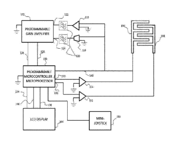
increase or
decrease voltage and frequency values. In some embodiments, the handheld
potentiostat 200
may comprise buttons or a keypad in addition to or instead of a mini-joystick
110. The
handheld potentiostat further comprises a working electrode port 202 and a
reference
electrode port 204. The electrode ports 202 and 204 are used to connect wire
leads to the
working and reference electrodes.
[0068] A block diagram representing one possible potentiostat /
electrode
configuration is found at FIG. 5. The heart of operation for the potentiostat
is carried out in
the programmable microcontroller/microprocessor 100. The first operation of
the
microcontroller is providing user interface support through an LCD display
104. The serial
peripheral interface 138 is used to communicate information processed in the
microcontroller
100 to the LCD display 104. The microcontroller 100 uses lines 134 and 136 to
supply
power to the LCD display 104.
[0069] User input/response to options displayed on the LCD display 104 is
received
as analog signals through an analog-analog communication between the mini-
joystick 110
and microcontroller 100. Using the mini-joystick 110, the user may select the
electrical
signal parameters, e.g., voltage, frequency, wave type, to be applied to the
working electrode
106 and reference electrode 108. Alternatively, the mini-joystick 110 is used
to select the
type of molecule to be detected. After the test concludes, the LCD display 104
shows the
numerical concentration of the molecule in the tested sample.
[0070] Next, the microcontroller 100 is programmed to perform
impedance
spectroscopy characterization on the attached electrochemical sensor. Based
upon the
electrical signal parameters or molecule selected by the user, the
programmable
microcontroller 100 generates an AC voltage on lines 130 and 132 that is
applied to the
working electrode 106 and reference electrode 108, respectively. The AC
voltage may be
amplified by amplifiers 112 and 114. In some embodiments, the resulting
voltage of the
working electrode 106 may fed back to the microcontroller 100 on line 140. The
resulting
voltage may differ from the applied voltage due to chemical reactions in the
tested solution.
The microcontroller 100 digitizes the voltage value of the working electrode
106, and the
digitized voltage is used by the microcontroller 100 to adjust the applied AC
voltage level on
lines 130 and 132. In some embodiments, the voltage of the working electrode
106 may fed
back to the programmable gain amplifier 102 on line 122. The programmable gain
amplifier
- 18-
CA 02919495 2016-01-26
WO 2015/017695 PCT/US2014/049228
may digitize the voltage value of the working electrode 106 and send the
digitized voltage to
the microcontroller 100 over line 128, and the digitized voltage is used by
the microcontroller
100 to adjust the AC voltage level on lines 130 and 132.
[0071] After an AC voltage is applied and a sample of an electrically
conductive
solution contacts the sensor, an AC current flows from the working electrode
106 to the
reference electrode 108. The amount of current flowing through the working
electrode 106
and reference electrode 108 depends upon the voltage applied to the working
and reference
electrodes, the binding of molecules on the electrodes, and the solution used.
A
programmable gain amplifier 102 measures the current flowing between the
working
electrode 106 and reference electrode 108. Specifically, the transconductance
amplifier 116
feeds a current to the programmable gain amplifier on line 124. The current
may be filtered
by a bandpass filter 120. The bandpass filter 120 is automatically adjusted to
permit signals
at the applied frequency while rejecting noise at other frequencies. The
programmable gain
amplifier 102 then generates an amplified voltage from the current that is fed
into the
programmable microcontroller on line 126. The amplification is necessary as
the
microcontroller operation thresholds are much greater than the small voltages
and currents
generated in this impedance spectroscopy application. In some embodiments, the
amplified
voltage on line 126 ranges between 20 mV and 6 V. If the amplified voltage on
line 126 is
too high or too low, the microcontroller 100 sends a signal to the
programmable gain
amplifier 102 over line 128 to increase or decrease the gain. In some
embodiments, the
binary gain of the programmable gain amplifier 102 may be adjusted between 1
and 128. In
some embodiments, the scope gain of the programmable gain amplifier 102 may be
adjusted
between 1 and 200. Line 122 provides a reference voltage to the programmable
gain
amplifier 102 to calculate gain. Line 122's voltage may be amplified by
amplifier 118 and
filtered by a bandpass filter 120.
[0072] The microcontroller 100 converts the analog amplified voltage
to a digital
signal. The microcontroller 100 then compares the digitized amplified voltage,
which
represents the amount of current flowing between working electrode 106 and
reference
electrode 108, to the voltage applied to the working electrode 106 and
reference electrode
108 to determine the impedance of the solution being tested. The
microcontroller 100
performs arithmetic operations to calculate phase and amplitude changes in the
amplified
voltage with respect to the applied voltage as a function of frequency.
Impedance is
calculated using the following formula:
- 19 -
CA 02919495 2016-01-26
WO 2015/017695 PCT/US2014/049228
Vm sin cut
Z =
linsin(wr + (p)
where Vm represents the amplitude of the applied voltage, Im represents the
amplitude of the
resulting current flowing between the electrodes, w is the angular frequency
of the applied
voltage and resulting current, and 9 is the difference in phase between the
applied voltage
and resulting current. In some embodiments, the microcontroller 100 uses a
Fourier
transform to determine the phase and amplitude changes as a function of
frequency. In some
embodiments, the microcontroller 100 uses Lissajous curves to determine the
phase and
amplitude changes. In some embodiments, the microcontroller 100 performs multi-
slice
splitting and signal analysis to determine at which frequencies the change in
impedance is the
greatest. This estimation helps in characterizing the bio-electrochemical
reactions occurring
on the surface of the electrodes. The microcontroller 100 uses the change in
amplitude and
phase to calculate the concentration of the molecule in the sample.
[0073] Before being used to measure unknown quantities of a target
analyte, the
handheld potentiostat may be calibrated. Calibration is performed by measuring
the
impedance of solutions containing known quantities of a target analyte.
Specifically, the user
may perfoun impedance measurements of preferably four different solutions
containing four
different concentrations of the target analyte. For each calibration test, the
user inputs the
target analyte concentration into the handheld potentiostat using the mini-
joystick. The
handheld potentiostat records the impedance for each test. After the tests are
completed, the
system completes the calibration by determining the coefficients in the
following equation,
zi = bid(' + bn_1xn-1+ . + bix + c
where zi is the measured impedance, x is the known concentration of the target
analyte, and
b1, and c are the coefficients. The order of the polynomial, n, may be between
two
and five, and preferably two. The handheld potentiostat determines the unknown
values of
the coefficients using linear regression and least squares analysis.
[0074] A flowchart depicting the detection of molecules using a
handheld potentiostat
is found at FIG. 9. At step 400, the user provides input, such as the choice
of voltage or
frequency, regarding the electrical signal that the handheld potentiostat will
apply to the
sample. At step 402, the microcontroller applies an electrical signal to the
working electrode
and reference electrode. The characteristics of the electrical signal, e.g.,
voltage and
frequency, are based upon the inputs provided by the user in step 400. At step
404, the
-20-
CA 02919495 2016-01-26
WO 2015/017695 PCT/US2014/049228
microcontroller receives a reference signal from the working electrode.
Specifically, the
working electrode voltage is amplified by a gain amplifier, and the amplified
voltage is fed
into the microcontroller's digital-to-analog converter ("DAC"), which converts
the analog
amplified voltage into a digital signal. In some embodiments, a programmable
gain amplifier
converts the analog amplified voltage into a digital signal. The
microcontroller compares the
value of the digital working electrode voltage to the desired voltage selected
by the user. The
microcontroller may then increase or decrease the applied electrical signal in
step 402 to
match the desired voltage that was selected in step 400. At step 406, the
working electrode
voltage value is fed into a gain amplifier and converted into a current. At
step 408, a gain
amplifier in the programmable gain amplifier amplifies the current signal and
converts the
current signal into a voltage signal. The voltage signal then enters the
micrcontroller's ADC.
At step 410, the microcontroller converts the analog voltage signal into a
digital voltage
signal. At step 412, the microcontroller compares the digital voltage signal
to calibration data
stored in the memory of the microcontroller. In some embodiments, the
microcontroller
compares the measures the analog voltage signal to stored calibration data. In
some
embodiments, the microcontroller compares the digital voltage signal to a
calibration data to
determine a difference in amplitude and phase as a function of frequency. In
some
embodiments, the microcontroller compares the digital voltage signal to a
calibration data to
determine a difference in amplitude and phase as a function of frequency. The
choice of
method depends on the noise level of the signal. Fourier transform is best
used when noise
signals are very high in the transmission lines.
[0075] In some embodiments, the microcontroller 100 is an Intel
microcontroller. In
other embodiments, the microcontroller 100 is an Intel microprocessor. In
other
embodiments, the microcontroller 100 is an ARM CortexTMM microcontroller. In
other
embodiments, the microcontroller 100 is an ARM CortexTM microprocessor.
[0076] In preferred embodiments, the microcontroller 100 applies an AC
voltage
between 1 mV and 10 V to the working electrode 106 and the reference electrode
108. The
microcontroller applies an AC voltage whose frequency varies between 2 Hz and
15 kHz to
the working electrode 106 and the reference electrode 108. The frequency is
varied by
increasing from a minimum to a maximum frequency or decreasing from a maximum
to a
minimum frequency. In some embodiments, the user selects a minimum and a
maximum
frequency, and the microcontroller 100 applies voltages having frequencies
that vary between
-21-
CA 02919495 2016-01-26
WO 2015/017695 PCT/US2014/049228
the selected minimum and maximum frequencies. In some embodiments, the
microcontroller
100 varies the frequency between the minimum and maximum frequencies in 2 Hz
intervals.
[0077] In some embodiments, the handheld potentiostats disclosed
herein perform
impedance spectroscopy analysis on a biosensing platform. Very low voltage is
necessary for
.. the use of these potentiostats in order to be applicable for biosensing, as
proteins and
biomolecules are sensitive. In some embodiments, the range of appropriate
voltage may be
may be 1 mV to 10 V, but the appropriate voltage will depend on the
application. In
applications to protein based sensing, the voltages will be in the range of 1
mV to 10 V. In
application to cells and DNA, the voltage ranges will be between 1 mV to 10 V.
Similarly,
due to the application of very small voltages, the current response is in a
similar range or
much lower, as there is loss due to bulk solution medium. In some embodiments,
the range
of appropriate current is 10 pA to 10 mA and, as with the voltage, the
appropriate current
response will depend on the application. In applications to protein based
sensing, the current
response will be in the range of 10 pA to 100 nA. In application to cells and
DNA, the
current response will be between 100 nA to 10 mA. The power required by the
handheld
potentiostat will be in the range of 2 mW to 10 W. The power level varies
based on the
casing, volume, time, analyte size, and the detection of single or multiple
analytes.
[0078] The disclosed potentiostats may be used at fixed or variable
frequencies.
Based on the application, the fixed and variable frequency ranges will vary.
For most
biosensing applications, the range of frequencies used is between 2 Hz and 15
kHz. Upon
optimization of the electrical debye length changes corresponding to a protein
of interest, the
fixed frequency can be estimated. Detection at the respective frequency can
improve
detection speeds and reduce non-specific signals.
[0079] In addition to performing impedance spectroscopy, the handheld
potentiostats
disclosed herein can be used as a source meter and also as a voltammetry tool
through easy-
to-choose options on the LCD display.
[0080] The handheld potentiostats disclosed herein are easily portable
and have a
hand friendly form factor. It may be about or at least 1, 2, 3, 4, 5, 6, 7, 8,
9, or 10 inches by
about or at least 1, 2, 3, 4, 5, 6, 7, 8, 9, or 10 inches. It is specifically
contemplated that it
may be about 5 inches by about 3 inches. It is also specifically contemplated
that the entire
device, including the programmable gain amplifier, the programmable
microcontroller, and
the LCD display for output that are indicated on the diagram, be within these
sizes.
- 22 -
CA 02919495 2016-01-26
WO 2015/017695 PCT/US2014/049228
[0081] A diagram depicting a smartphone embodiment of the handheld
potentiostat is
found at FIG. 10. The handheld potentiostat comprises a smartphone 300 and a
potentiostat
adaptor 306. The smartphone is operably coupled to a potentiostat adaptor 306
using a cable
304, preferably a Micro USB or a proprietary connector. The cable 304 provides
bi-
directional communication between the smartphone 300 and the potentiostat
adaptor 306.
The potentiostat adaptor comprises a working electrode port 202, a reference
electrode port
204, a microcontroller 100, and a programmable gain amplifier 102. Users
install a custom
potentiostat software application onto the smartphone 300 that provides user
input and output
and microcontroller communication functionality. Users may provide input to
the
smartphone 300, including the input voltage, input frequency, and wave type,
using a
touchscreen 302. In other embodiments, users provide input to the smartphone
using a
keypad. The smartphone 300 displays output, such as the concentration of the
target analyte
on the smartphone's touchscreen 302.
[0082] The potentiostats disclosed herein also perform with low noise
threshold at the
desired range of operation for biosensing. Currently, potentiostats are
designed with
electrochemical applications in mind. The integrated circuits used for these
applications have
reasonable noise thresholds. When applying to bioscnsing, the measured signals
of the
available devices are in many cases within the noise threshold, thus rendering
majority of the
available potentiostats unsuitable.
[0083] The potentiostats disclosed herein are also programmable to perform
two
electrode impedance spectroscopy using Fourier transforms and Lissajous curve
method.
Existing potentiostats use Lissajous curves methods to estimate phase change
in the measured
current response. Though this has been perfected for applications involving
high voltages and
currents, it is not optimized for analysis of voltage and current responses as
necessary for
biosensing. Fourier transform-based estimation, which is more appropriate for
these
applications, has not been widely used due to complexity in implementation as
it demands
high processor speeds. Using Lissajous curves and Fourier transforms assists
in digital signal
analysis by reducing noise and preserving signal integrity; both of which are
critical for
biosensing.
[0084] A flowchart demonstrating the potentiostat's calculations using
Fourier
transforms and Lissajous curves is shown at Fig. 11. At step 500, the
microcontroller applies
a sinusoidal voltage of the form V (t) = v sin(wt), where v is the amplitude
of the signal and
co is the angular frequency. In preferred embodiments, the microcontroller
applies sinusoidal
- 23 -
CA 02919495 2016-01-26
WO 2015/017695 PCT/US2014/049228
voltages at varying frequencies. At step 502, the microcontroller measures the
resulting
current signal, which is of the form 1(t) = i sin(wt + (p), where i is the
amplitude of the
signal and p is the phase shift of the signal. The microcontroller converts
the applied voltage
signal from the time domain into the frequency domain in step 504 by applying
a Fourier
transform, V(w) = -T1 f v(t)eiwt dt. Likewise, the microcontroller converts
the resulting
current signal from the time domain into the frequency domain in step 506 by
applying a
Fourier transform, 1((o) f i
(t)eiwt dt. At step 508, the resulting current frequency
signal is verified with the applied voltage signal and noise occurring at
other frequencies is
filtered out. As an alternative to steps 504-510, the microcontroller plots
Lissajous curves of
v(t) and i(t) to estimate the impedance Z(t) at step 512. Fig. 12 illustrates
a sample Lissajous
curve, where E represents the applied voltage and I represents the resulting
current. In this
example, the applied voltage is a sinusoidal wave that varies between 15 and -
15 mV, and the
resulting current varies between 45 and 55 nA. The intersection of the voltage
and current on
the plot in this example is an ellipse, which indicates that the system is
stable. Analysis of
the elliptical region provides an estimate of the resulting impedance. At step
514, the
microcontroller coverts impedance to the frequency domain using the equation
Z(w) =
f Z(t)ei't dt. At step 516, the microcontroller calculates the change in
impedance,
AZ(03), using the formula AZ(w) = Zb(w) ¨ Z(w), where Zh(co) is the impedance
of the
control sample. At step 518, the microcontroller determines the frequency at
which the
maximum impedance change occurred using multi-slice splitting, wherein the
applied
frequency spectrum is sliced into individual discrete frequency points. The
microcontroller
then compares the frequency at which the maximum impedance change occurred to
the
reference frequency point stored in memory for the specific analyte being
tested at step 520.
At step 522, the microcontroller estimates the concentration of the tested
analyte by applying
the same equation used in calibration, zi = bnxn + brt-1xn-1+ ...+ bix + c,
where zi is the
impedance at the frequency at which the maximum impedance change occurred, and
bn, 1)11_1,
b1, and c are coefficients calculated during calibration, and x is the target
analyte
concentration being computed. In preferred embodiments, the equation in step
522 is
quadratic. Step 524 illustrates the change in impedance as a function of
target analyte
concentration.
[0085] The
potentiostats disclosed herein also contain cost-effective components,
manufacturing involves very simple surface mount device assembly, and the
disclosed
- 24 -
CA 02919495 2016-01-26
WO 2015/017695 PCT/US2014/049228
devices have low-thermal noise due to use of modern current amplifiers and
programmable
gate arrays.
[0086] Finally, the potentiostats disclosed herein have applicability
as a source meter,
a voltammetry tool, and for standard current measurements. The potentiostats
can be
customized for the different applications by making modifications to the
program that run the
operations and produce results. The programmable gain amplifiers have a broad
range of
operation (mV¨V/pA-mA) and hence can be used for different voltammetry
applications to
biosensing as well as general applications. Microprocessors/microcontrollers
offer extensive
programming liberties and hence application of the potentiostats to different
operations will
require only software changes and not hardware.
[0087] The potentiostats disclosed herein arc highly adaptable and
generates results
rapidly. For a single channel assay, when a single channel EIS detection
scheme and a 16-bit
microcontroller (40-10kHz) is used, it results in a read time of less than 40
seconds.
E. Kits
[0088] In some embodiments, contemplated are kits comprising conformal
circuits
and a potentiostat. In some embodiments, these kits are designed to
accommodate a
particular target analyte, e.g., a particular protein of interest. In one
embodiment, the kit will
comprise conformal circuits comprising a nanotextured porous substrate which
is appropriate
for the target analyte, which will have an appropriate pattern transferred to
it, where the
pattern is made up of an appropriate ink. In addition, the kit will further
comprise a
potentiostat which is calibrated to generate the data of interest to the user
for the particular
target analyte.
[0089] The following table illustrates examples of capture probes for
which the kit
may detect, the frequency of the applied electric field, the membrane type,
the pore size of
the membrane, and the power required:
Frequency of electric
Type of Pore size of Power
field for Helmholtz Substrate type
capture probe membrane required
probing
Antibody -
4 Hz 5 kHz Track etched, acid
0.1 1.tm ¨ 0.5 im 2 mW - 10 W
monoclonal etched, anodized,
polymer, ceramic and
- 25 -
CA 02919495 2016-01-26
WO 2015/017695 PCT/US2014/049228
Antibody - electro deposited
4 Hz - 5 kHz 0.1 m -0.5 p.m 2 mW - 10
W
polyelonal
Apt amer -
4 Hz - 5 kHz 0.05 pin -0.2 m 2 mW - 10
W
RNA
Aptamer -
7.5 Hz - 5 kHz 0.1 um - 0.5 p.m 6 mW - 10
W
protein
Protein 4.8 Hz 5 kHz 0.1 in 0.5 um 2 mW 10 W
Sugar 4 Hz - 5 kHz 0.03 m -0.1 m 2 mW - low
DNA 4 Hz - 5 kHz 0.05 in - 0.3 in 3 mW -
9 W
RNA 4 Hz - 5 kHz 0.05 p.m -0.3 m 4 mW - 10
W
Steroids 4 Hz - 5 kHz 0.03 lint - 0.1 m 2 rnW -
10 W
Cholesterol 4 Hz - 5 kHz 0.03 m - 0.111111 2 mW -
10 W
[0090] For example, a confolinal circuit designed to detect C-reactive
protein would
have a substrate of nanoporous material, e.g., paper, having a porosity of 10"
to 10"
pores/cm2 of 200 nm pores, where the circuit is made of a pattern that is
interdigitated or
edge-free interdigitated, or a concentric ring made using metal nanoparticle-
infused carbon
ink infused with gold/platinum/silver/copper/nickel. The parameters of
interest that would be
inputed into the potentiostat include the applied voltage of 10 mV and an
applied frequency
and range of 20 Hz to 10 kHz. Finally, the parameters of interest for analysis
include the
frequency of analysis, applied voltage, current measured, calculated
impedance, estimated
concentration, and standard calibration curve.
F. Examples
[0091] The following examples are included to demonstrate preferred
embodiments
of the invention. It should be appreciated by those of skill in the art that
the techniques
disclosed in the examples which follow represent techniques discovered by the
inventor to
function well in the practice of the invention, and thus can be considered to
constitute
preferred modes for its practice. However, those of skill in the art should,
in light of the
present disclosure, appreciate that many changes can be made in the specific
embodiments
-26-
CA 02919495 2016-01-26
WO 2015/017695 PCT/US2014/049228
which are disclosed and still obtain a like or similar result without
departing from the spirit
and scope of the invention.
EXAMPLE 1
[0092] This assay has been used in the impedance format towards
detecting
Troponin-T in human serum. 0.1 pgimL sensitivity has been achieved. Multiple
replicates
with data collected over a ninety day period is shown in FIG. 2. The circuit
utilized a comb-
based interdigitated electrical circuit, but any rectilinear combination of
working and
reference electrode is suitable for this application. The substrate was a
nanoporous nylon
membrane and the pattern was made using cryo-evaporation of gold ink, also
known as gold
sputtering, which is an additive deposition technique. Sample volume was 1 to
10
microliters. The circuit was connected to the impedance reader and a bias
potential in the
millivolt regime is applied and the change in impedance due to the step-wise
introduction of
the various components of the assay, linker, molecules, receptor, and ligand
produces a step-
wise measurable impedance change.
[0093] To calibrate the device, the inventors first deposited a thiol based
linker that
can effectively bind to the gold electrode. DSP dissolved in DMSO was used. A
sulfur bond
is formed with the gold electrode and an open amine end is left for
protein/biomolecule
immobilization. Following this, the inventors saturated the linker deposited
sensor surface
with monoclonal Troponin-T antibody. A buffer wash was performed to remove
excess
antibodies. Next, a blocking buffer consisting of albumin was used to close
off all non-
antibody immobilized linker molecules. This effectively helps in reducing
noise signals due
to non-specific binding of target analytes to linker sites. A buffer wash was
performed to
remove excess blocker molecules. The step is the baseline point or control
step of the assay
where zero dose of antigen is present. Antigen doses, in this case Troponin-T,
were prepared
in buffer media in increasing logarithmic doses. The buffer media used was
phosphate buffer
solution, human serum, and human plasma. Troponon-T antigen doses were spotted
on the
sensor surface one by one in the order of increasing concentration. Spotting
refers to
inoculation, pipetting out, or application of a sample on the sensor
substrate. Impedance
measurements were performed at each step of the assay. Impedance measurements
were
calculated as the ratio between applied voltage and measured current response
at different
frequency points in the range of 2 Hz to 15 kHz. The maximum impedance change
occurred
at 100.4 Hz. The impedance as a function of frequency was calculated using a
Fourier
transform. Applying a voltage having a frequency in which the greatest
impedance change
- 27 -
CA 02919495 2016-01-26
WO 2015/017695 PCT/US2014/049228
occurred, the change in impedance was calculated for every dose as the
difference between
impedance at baseline and at the current dose being measured. A calibration
response curve
was built by plotting the change in impedance and troponin-T antigen
concentration. A
quadratic equation was used to fit the calibration response curve. This
fitting study resulted
in a polynomial calibration equation that was used for estimating
concentration of Troponin-
T from test samples. For testing samples and estimating concentration of
Troponin-T, the
following assay protocol was used. The thiol based linker molecules were first
deposited on
the sensor surface. Monoclonal antibodies specific to Troponin-T was used for
the detection.
A blocking buffer was used to seal-off non-specific binding sites. Buffer
washes were
performed at intermediate steps to remove excess molecules not bound to the
surface. The
impedance measurement carried out at the buffer wash after blocking buffer
application was
used as the baseline or control impedance. Following this, test samples were
applied to the
sensor surface and impedance measurements were carried out. The test sample's
impedance
was calculated and was used in the quadratic equation discussed above to
estimate the
concentration of Troponin-T in the test samples. There was a dose dependent
change to the
measured impedance.
[0094] The metallic switch behavior of the conformal circuit has been
mapped
towards detecting trace pesticides at ultra-low concentrations. As a
representative example,
detection of atrazine has been demonstrated when spiked in municipal water
supply. The data
has been obtained from multiple replicates collected over a thirty day period
(FIG. 3). The
conformal circuit works like an AND gate. There are two inputs to the circuit
and one
output. When the input region of the circuit contains only the receptor or the
ligand, then the
output will remain low. However, in the presence of both the antibody and the
small
molecule, the output will be high, showing the turn ¨on of the metallic switch
reaching its
threshold voltage resulting in a current measurement in the micro amps range
at the output.
The volume used for this assay was 1 to 10 microliters.
[0095] The transfer characteristics for non-linear two terminal device
behavior have
been demonstrated for detecting DNA. The change in transfer charge or
transconductance for
various biasing voltages for the target and the associated back ground has
been demonstrated
(FIG. 4). The width of the conducting channel in the conformal circuit was
varied and hence
its current carrying capability. The width is varied due to the interaction of
the targeted
ligands with receptors immobilized on the semiconducting surfaces of the
circuit. Surface
modification is achieved using carboxylic, hydroxlie, sulfur, or amine based
chemistries.
-28-
CA 02919495 2016-01-26
WO 2015/017695 PCT/US2014/049228
Binding of the targeted species modulates the channel current. For a specific
applied bias
potential, the current carrying capacity of the channel is modulated by the
dose dependent
interactions of the targeted molecules onto the circuit. The volume used to
perform this
assay was 1 to 10 microliters.
EXAMPLE 2
[0096] Samples of miR21 enriched cells were tested on a paper
cartridge, using a
twenty base pair oligo-target miR21. Wild type cells were used as a control.
The relative
concentration of miR21 was high, i.e., greater than 200 copies/cell. These
measurements
were made by a nucleic acid-based sensor. The sensor was prepared by first
generating the
miR21 probe by in vitro transcription from a plasmid harboring a cDNA of the
mature
microRNA. The conformal circuit was made of a nanoporous nylon membrane
patterned
using cryo-evaporation with gold ink. The nucleic acid probe, complementary to
a region of
miR21, was bound to the gold electrode. In the electrical oligonucleotide
assay protocol, this
configuration permitted capture, detection, and quantification of miR21 in RNA
isolates
from cell lysates.
EXAMPLE 3
[0097] Septicemia: Samples taken from patients to diagnosis the
pathogenic basis of
septicemia. Markers were used for lipopolysaccaride (indicator of gram
negative bacteria),
lipoteichoie acid (indicator of gram positive bacteria), and procalcitonin
(marker of severe
sepsis caused by bacteria and generally grades well with the degree of
sepsis). Samples
included five whole blood samples from ICU patients who had a clinical
confirmation of
septicemia.
[0098] To calibrate the device, the inventors first deposited a thiol
based linker that
can effectively bind to the gold electrode. DSP dissolved in DMSO was used. A
sulfur bond
is formed with the gold electrode and an open amine end is left for
protein/biomolecule
immobilization. Following this, the inventors saturated the linker deposited
sensor surface
with monoclonal antibodies for lipopolysaccharide, lipoteichoic acid, and
procalcitonin. A
buffer wash was performed to remove excess antibodies. Next, a blocking buffer
consisting
of albumin was used to close off all non-antibody immobilized linker
molecules. This
effectively helps in reducing noise signals due to non-specific binding of
target analytes to
linker sites. A buffer wash was performed to remove excess blocker molecules.
This is the
baseline point or control step of the assay where zero dose of antigen is
present.
-29-
CA 02919495 2016-01-26
WO 2015/017695 PCT/US2014/049228
Antigen/protein biomarker doses were prepared in buffer media in increasing
logarithmic
doses. The buffer media used was phosphate buffer solution, human serum, and
human
plasma. Each of these buffer media were applied to a separate sensor.
Antigen/protein
biomarker doses were spotted on the sensor surface one by one in the order of
increasing
concentration. Impedance measurements were performed at each step of the
assay.
Impedance measurements were calculated as the ratio between applied voltage
and measured
current response at different frequency points in the range of 2 Hz to 15 kHz.
Lipopolysaccharides showed the greatest impedance change at 99.3 Hz,
lipoteichoic acid
showed the greatest impedance change at 120 Hz, and procalcitonin showed the
greatest
impedance change at 110 Hz. The impedance as a function of frequency was
calculated
using a Fourier transform. Applying a voltage having a frequency in which the
greatest
impedance change occurred, the change in impedance was calculated for every
dose as the
difference between impedance at baseline and at the current dose being
measured. A
calibration response curve was built by plotting the change in impedance and
antigen
concentration. A quadratic equation was used to fit the calibration response
curve. This fitting
study resulted in a polynomial calibration equation that was used for
estimating concentration
of antigen/protein biomarkers from test samples. For testing samples and
estimating
concentration of the protein biomarkers, the following assay protocol was
used. The thiol
based linker molecules were first deposited on the sensor surface. Monoclonal
antibodies
specific to the protein biomarkers were used for the detection. A blocking
buffer was used to
seal-off non-specific binding sites. Buffer washes were performed at
intermediate steps to
remove excess molecules not bound to the surface. The impedance measurement
carried out
at the buffer wash after blocking buffer application was used as the baseline
or control
impedance. Following this, test samples were applied to the sensor surface and
impedance
measurements were carried out. The test sample's impedance was calculated and
was used in
the quadratic equation discussed above to estimate the concentration of the
protein
biomarkers in the test samples.
[0099] Quantitative results were obtained in less than twenty minutes,
with the lowest
detection limit for the markers at 10 fg/mL. See Table 1. A correlation of
severe septicemia
to high levels of procalcitonin was identified.
Table 1
Procalcitonin Lipopolysaccharide - pg/mL Lipoteichoic acid -
pg/mL
Sample (pg/rriL) (gram negative bacteria) ,
(gram positive bacteria) Clinical data
I _ 0.026 0.08 <0.01 Yes
- 30 -
CA 02919495 2016-01-26
WO 2015/017695 PCT/US2014/049228
2 43.97 0.93 12.6 Yes
3 126.83 18.64 184.91 Yes
4 635.99 194.60 340.44
Yes, severe
1794 991.00 3716 Yes, severe
[00100] The conformal circuit was made of a nanoporous nylon membrane
patterned
using cryo-evaporation with gold ink. The protocol used was an electrical
immunoassay
protocol which involves binding a protein specific monoclonal antibody to the
substrate
5 .. electrodes. Blood samples from patients who were suspected with septic
infection were
collected. These were tested for three different markers Procalcitonin,
Lipopolysaccharide
and Lipoteichoic acid. The detection was performed by studying impedance
changes as a
result of specific protein markers binding to the immobilized capture
antibodies on the
surface of the electrodes.
[00101] Cardiovascular markers: Twelve human plasma samples from patients
who
have had myocardial infarction events were tested to quantify troponin-T
(cardiac marker) for
analyzing its behavior and reliability as a marker for early diagnosis.
[00102] To calibrate the device, the inventors first deposited a thiol
based linker that
can effectively bind to the gold electrode. DSP dissolved in DMSO was used. A
sulfur bond
is formed with the gold electrode and an open amine end is left for
protein/biomolecule
immobilization. Following this, the inventors saturated the linker deposited
sensor surface
with monoclonal Troponin-T antibody. A buffer wash was performed to remove
excess
antibodies. Next, a blocking buffer consisting of albumin was used to close
off all non-
antibody immobilized linker molecules. This effectively helps in reducing
noise signals due
to non-specific binding of target analytes to linker sites. A buffer wash was
performed to
remove excess blocker molecules. The step is the baseline point or control
step of the assay
where zero dose of antigen is present. Antigen doses, in this case Troponin-T,
was prepared
in buffer media in increasing logarithmic doses. The buffer media used was
phosphate buffer
solution, human serum and human plasma. Troponin-T antigen doses were spotted
on the
.. sensor surface one by one in the order of increasing concentration.
Impedance measurements
were performed at each step of the assay. Impedance measurements were
calculated as the
ratio between applied voltage and measured current response at different
frequency points in
the range of 2 Hz to 15 kHz. The impedance as a function of frequency was
calculated using
a Fourier transform. Applying a voltage having a frequency in which the
greatest impedance
-31 -
CA 02919495 2016-01-26
WO 2015/017695 PCT/US2014/049228
change occurred, the change in impedance was calculated for every dose as the
difference
between impedance at baseline and at the current dose being measured. A
calibration
response curve was built by plotting the change in impedance and troponin-T
antigen
concentration. A quadratic equation was used to fit the calibration response
curve. This fitting
study resulted in a polynomial calibration equation that was used for
estimating concentration
of Troponin-T from test samples. For testing samples and estimating
concentration of
Troponin-T, the following assay protocol was used. The thiol based linker
molecules were
first deposited on the sensor surface. Monoclonal antibodies specific to
Troponin-T was used
for the detection. A blocking buffer was used to seal-off non-specific binding
sites. Buffer
washes were performed at intermediate steps to remove excess molecules not
bound to the
surface. The impedance measurement carried out at the buffer wash after
blocking buffer
application was used as the baseline or control impedance. Following this,
test samples were
applied to the sensor surface and impedance measurements were carried out. The
test
sample's impedance was calculated and was used in the quadratic equation
discussed above
to estimate the concentration of the protein biomarkers in the test samples.
[00103] The lowest detected dose was 0.71 pg/mL, which is three orders
of magnitude
more sensitive than ELISA for this marker. FIG. 6. The conformal circuit was
made of a
nanoporous nylon membrane patterned using cryo-evaporation with gold ink. The
protocol
used was an electrical immunoassay protocol which involves binding a protein
specific
monoclonal antibody to the substrate electrodes. En this case, it was antibody
to Troponin-T
protein biomarker. Plasma samples from twelve patients were collected. These
samples were
applied to the sensing substrate. The presence and amount of troponin-T were
quantified by
measuring the impedance response as a result of Troponin-T binding to the
antibodies
immobilized on the electrode surface.
[00104] Cancer markers: Ten human scrum matrix samples spiked with prostate-
specific antigen (PSA) were tested to quantify PSA for its use in diagnosis of
prostate cancer.
[00105] To calibrate the device, the inventors first deposited a thiol
based linker that
can effectively bind to the gold electrode. DSP dissolved in DMSO was used. A
sulfur bond
is formed with the gold electrode and an open amine end is left for
protein/biomolecule
immobilization. Following this, the inventors saturated the linker deposited
sensor surface
with monoclonal prostate specific antigen antibody. A buffer wash was
performed to remove
excess antibodies. Next, a blocking buffer consisting of bovine serum albumin
with
proprietary thermoscientific reagents was used to close off all non-antibody
immobilized
- 32 -
CA 02919495 2016-01-26
WO 2015/017695 PCT/US2014/049228
linker molecules. This effectively helps in reducing noise signals due to non-
specific binding
of target analytes to linker sites. A buffer wash was performed to remove
excess blocker
molecules. The step is the baseline point or control step of the assay where
zero dose of
antigen is present. Antigen doses, in this case, prostate specific antigen was
prepared in
buffer media in increasing logarithmic doses. The buffer media used was
phosphate buffer
solution, human serum matrix and human plasma. Prostate specific antigen doses
were
spotted on the sensor surface one by one in the order of increasing
concentration. Impedance
measurements were performed at each step of the assay. Impedance measurements
were
calculated as the ratio between applied voltage and measured current response
at different
frequency points in the range of 2 Hz to 15 kHz. The impedance as a function
of frequency
was calculated using a Fourier transform. PSA showed the greatest impedance
change at
128.4 Hz. Applying a voltage having a frequency in which the greatest
impedance change
occurred, the change in impedance was calculated for every dose as the
difference between
impedance at baseline and at the current dose being measured. A calibration
response curve
was built by plotting the change impedance and prostate specific antigen
concentration. A
quadratic equation was used to fit the calibration response curve. This
fitting study resulted in
a polynomial calibration equation that was used for estimating concentration
of prostate
specific antigen from test samples. For testing samples and estimating
concentration of
prostate specific antigen, the following assay protocol was used. The thiol
based linker
molecules were first deposited on the sensor surface. Monoclonal antibodies
specific to
prostate specific antigen was used for the detection. A blocking buffer was
used to seal-off
non-specific binding sites. Buffer washes were performed at intethiediate
steps to remove
excess molecules not bound to the surface. The impedance measurement carried
out at the
buffer wash after blocking buffer application was used as the baseline or
control impedance.
Following this, test samples were applied to the sensor surface and impedance
measurements
were carried out. The test sample's impedance was calculated and was used in
the quadratic
equation discussed above to estimate the concentration of the protein
biomarkers in the test
samples.
[00106] The lowest detected dose was 0.0052 ng/mL. FIG. 7. The
conformal circuit
was made of a nanoporous nylon membrane patterned using cryo-evaporation with
gold ink.
The protocol used was an electrical immunoassay protocol which involves
binding a protein
specific monoclonal antibody to the substrate electrodes. In this case, it was
antibody to
prostate specific antigen biomarker. Human scrum matrix samples were prepared
and spiked
- 33 -
CA 02919495 2016-01-26
WO 2015/017695 PCT/US2014/049228
with different concentrations of prostate specific antigen. These samples were
applied to the
sensing substrate. The presence and amount of Prostate specific antigen were
quantified by
measuring the impedance response as a result of prostate specific antigen
binding to the
antibodies immobilized on the electrode surface.
[00107] Fungicide detection: 6 juice samples spiked with strobulrin
fungicides were
tested to quantify the level of strobulrin in the sample. The lowest detected
dose was 10 pM.
Table 2.
Table 2
Spectrophotometry impress Spectrophotometry
impress
Sample (Trifloxystrobin) (Trifloxystrobin) (Azoxystrobin) (Azoxystrobin)
1 Cannot be detected 10 pM Cannot be
detected 13 pM
2 101 pM 100 pM 125 pM 126.2 pM
3 150 pM 150 pM 142 oM 144 pM
4 10 nM 10 nM 19 nM 19.2 nM
5 100 nM 100 nM 100 nM 100 nM
6 1000 nM 1000 nM 800 nM 800 nM
[00108] The conformal circuit was made of a nanoporous nylon membrane
patterned
using cryo-evaporation with gold ink. The protocol used was an electrical
immunoassay
protocol which involves binding a fungicide specific antibody or aptamer to
the sensing
substrate. Fresh juice samples spiked with various concentrations of the
mentioned fungicides
were taken and applied to the sensor substrate.
[00109] To calibrate the device, the inventors first deposited a thiol
based linker that
can effectively bind to the gold electrode. DSP dissolved in DMSO was used. A
sulfur bond
is formed with the gold electrode and an open amine end is left for
protein/biomolecule
immobilization. Following this, the inventors saturated the linker deposited
sensor surface
with monoclonal antibodies or aptamers. A buffer wash was performed to remove
excess
antibodies. Next, a blocking buffer consisting of albumin was used to close
off all non-
antibody immobilized linker molecules. This effectively helps in reducing
noise signals due
to non-specific binding of target analytes to linker sites. A buffer wash was
performed to
remove excess blocker molecules. The step is the baseline point or control
step of the assay
where zero dose of antigen is present. Fungicide doses were prepared in buffer
media in
.. increasing logarithmic doses. The buffer media used was phosphate buffer
solution, water or
juice varieties. Fungicide doses were spotted on the sensor surface one by one
in the order of
- 34 -
CA 02919495 2016-01-26
WO 2015/017695 PCT/US2014/049228
increasing concentration. Impedance measurements were performed at each step
of the assay.
Impedance measurements were calculated as the ratio between applied voltage
and measured
current response at different frequency points in the range of 2 Hz to 15 kHz.
The impedance
as a function of frequency was calculated using a Fourier transform. Fungicide
showed the
greatest impedance change at 104 Hz. Applying a voltage having a frequency in
which the
greatest impedance change occurred, the change in impedance was calculated for
every dose
as the difference between impedance at baseline and at the current dose being
measured. A
calibration response curve was built by plotting change in impedance and
fungicide
concentration. A quadratic equation was used to fit the calibration response
curve. This fitting
study resulted in a polynomial calibration equation that was used for
estimating concentration
of fungicide from test samples. For testing samples and estimating
concentration of fungicide,
the following assay protocol was used. The thiol based linker molecules were
first deposited
on the sensor surface. Monoclonal antibodies specific to fungicides was used
for the
detection. A blocking buffer was used to seal-off non-specific binding sites.
Buffer washes
were performed at intermediate steps to remove excess molecules not bound to
the surface.
The impedance measurement carried out at the buffer wash after blocking buffer
application
was used as the baseline or control impedance. Following this, test samples
were applied to
the sensor surface and impedance measurements were carried out. The test
sample's
impedance was calculated and was used in the quadratic equation discussed
above to estimate
the concentration of the protein biomarkers in the test samples.
[00110] The presence of the various fungicides was detected and
quantified by
measuring the impedance changes as a result of fungicide binding to the
aptamers or
antibodies immobilized on the electrode surface. Aptamers, or oligonucleotide
probes, can
used for capture and detection of biomarkers and biomolecules.
* * *
[00111] All of the methods disclosed and claimed herein can be made and
executed
without undue experimentation in light of the present disclosure. While the
compositions and
methods of this invention have been described in terms of preferred
embodiments, it will be
apparent to those of skill in the art that variations may be applied to the
methods and in the
steps or in the sequence of steps of the method described herein without
departing from the
concept, spirit and scope of the invention. More specifically, it will be
apparent that certain
agents which are both chemically and physiologically related may be
substituted for the
agents described herein while the same or similar results would be achieved.
All such similar
- 35 -
CA 02919495 2016-01-26
WO 2015/017695 PCT/US2014/049228
substitutes and modifications apparent to those skilled in the art are deemed
to be within the
spirit, scope and concept of the invention as defined by the appended claims.
- 36 -
WO 2015/017695
PCT/US2014/049228
REFERENCES
The following references provide exemplary procedural or other details
supplementary to
those set forth herein.
Reighard & Barendt, "Conformal Coating Process Controls: The Manufacturing
Engineer's Aid."
APEX Long Beach, CA. March 2000.
Vestergaard, et al., Sensors. 7(12):3442-58, 2007.
- 37 -
Date Recue/Date Received 2021-01-15