Note : Les descriptions sont présentées dans la langue officielle dans laquelle elles ont été soumises.
CA 02968375 2017-05-18
WO 2016/081775 PCT/US2015/061690
VOLUMETRIC ELECTROMAGNETIC COMPONENTS
RELATED APPLICATIONS
[0001] This application is a continuation-in-part of U.S. Application No.
14/629,032, titled "Method and Apparatus for Folded Antenna Components," filed
23
February 2015. This application claims priority to and the benefit of U.S.
Provisional
Application No. 61/996,347 filed February 22, 2014 and entitled "Method and
Apparatus for Folded Antenna Components"; this application also claims
priority to
U.S. Provisional Patent Application No. 62/123,579, titled "Structure Embedded
Electromagnetic Absorbers," filed 20 November 2014; this application also
claims
priority to and the benefit of U.S. Provisional Patent Application No.
62/123,581,
titled "Method and Apparatus for Folded Volumetric Electromagnetic
Components,"
filed 20 November 2014; the entire contents of all of which applications are
incorporated herein by reference.
BACKGROUND
[0002] Antennas are used to typically radiate and/or receive
electromagnetic
signals, preferably with antenna gain, directivity, and efficiency. Practical
antenna
design traditionally involves trade-offs between various parameters, including
antenna gain, size, efficiency, and bandwidth.
[0003] Antenna design has historically been dominated by Euclidean
geometry.
In such designs, the closed area of the antenna is directly proportional to
the
antenna perimeter. For example, if one doubles the length of a Euclidean
square (or
"quad") antenna, the enclosed area of the antenna quadruples. Classical
antenna
design has dealt with planes, circles, triangles, squares, ellipses,
rectangles,
hemispheres, paraboloids, and the like.
[0004] With respect to antennas, prior art design philosophy has been to
pick a
Euclidean geometric construction, e.g., a quad, and to explore its radiation
characteristics, especially with emphasis on frequency resonance and power
patterns. Unfortunately antenna design has concentrated on the ease of antenna
construction, rather than on the underlying electromagnetics, which can cause
a
reduction in antenna performance.
1
CA 02968375 2017-05-18
WO 2016/081775 PCT/US2015/061690
[0005]
Practical antenna design traditionally involves trade-offs between various
parameters, including antenna gain, size, efficiency, and bandwidth. Antenna
size is
also traded off during antenna design that typically reduces frequency
bandwidth.
Being held to particular size constraints, the bandwidth performance for
antenna
designs such as discone and bicone antennas is sacrificed resulted in reduced
bandwidth.
[0006]
Dipole-like antenna have used a bicone or discone shape to afford the
performance desired over a large pass band. For example, some pass bands
desired exceed 3:1 as a ratio of lowest to highest frequencies of operation,
and
typically ratios of 20:1 to 100:1 are desired. Some prior art discone antennas
have
included a sub-element shaped as a cone whose apex is attached to one side of
a
feed system at location. A second sub-element can be attached to the other
side of
the feed system, such as the braid of a coaxial feed system. This sub-element
is a
flat disk meant to act as a counterpoise.
[0007]
Both discone and bicone antennas afford wideband performance often
over a large ratio of frequencies of operation; in some arrangements more than
10:1.
However, such antennas are often 1/4 wavelength across, as provided by the
longest
operational wavelength of use, or the lowest operating frequency. In height,
the
discone is typically 1/4 wavelength and the bicone almost 1/2 wavelength of
the longest
operational wavelength.
Typically, when the lowest operational frequency
corresponds to a relatively long wavelength, the size and form factor of these
antenna becomes cumbersome and often prohibitive for many applications.
[0008]
Antenna systems that incorporate a Euclidean geometry include roof-
mounted antennas that extend from objects such as residential homes or
automobiles. Such extendable antennas can be susceptible to wind and other
weather conditions and may be limited in bandwidth and frequency range.
Additionally, by implementing a Euclidean geometry into these conformal
antennas,
antenna performance is degraded.
-2-
CA 02968375 2017-05-18
WO 2016/081775 PCT/US2015/061690
SUMMARY
[0009] This disclosure relates to systems, apparatus, and methods using
three-
dimensional, or volumetric, components to interact with energy in a desired
manner,
e.g., absorb, guide, transmit, and/or receive.
[0010] In accordance with an aspect of the disclosure, methods are
disclosed for
making antenna apparatus, components, and related or ancillary components
suitable for wideband transmission and reception. An example of such an
antenna
apparatus can include a bicone antenna portion (bicone antenna) including two
cone-shaped elements (e.g., an accordioned bicone antenna) or a reverse bi-
cone
antenna, have a general shape where the two open ends of the cones are joined
(directly or via an intermediate shape). The physical shape of at least one of
the two
cone-shaped elements may be at least partially defined by one or more folds
(e.g., a
series) that extend about a portion of the cone. Other shapes and
configurations
such as those including self-similar features can be included for the antennas
or
components.
[0011] Exemplary embodiments include a novel system and method for
producing
such antenna parts and antennas made by same, is also disclosed. The system
may
utilize a material accretion device, such as a three-dimensional (3D) printer,
to make
volumetric plastic components that incorporate one or more folds and/or have
self-
similar structure (fractal in finite iterations for at least a portion) for at
least part of the
component. The component may be constructed out of conductive plastic, or non-
conductive plastic.
[0012] If non-conductive plastic is used, the component may be coated,
plated,
painted or gilded with a conductor (such as conductive paint) after printing
so the
component then conducts and can act as an antenna component. These
components may be actual radiators, filters, counterpoises ground planes, or
loads.
Dipoles, monopoles, dielectric resonators, leaky antennas, metamaterial
antennas,
metasurface antennas, slot antennas, cavity antennas, and many other kinds of
antennas may be made in this system. The antennas may have smaller size and or
better gain and or greater bandwidths than antennas of conventional design.
They
may be used from 50-6000 MHz or any fraction of same bandwidth. They may be
-3-
CA 02968375 2017-05-18
WO 2016/081775 PCT/US2015/061690
used in telematics; wireless, cell phone communication, WIFI, Wimax, UWB, and
other systems.
[0013] A further aspect of the present disclosure is directed to systems
and
methods for producing volumetric electromagnetic components, and volumetric
electromagnetic components made by same. Such volumetric electromagnetic
components can take function as waveguides, absorbers, attenuators and/or
other
electromagnetic components. In exemplary embodiments, such volumetric
electromagnetic components can be embedded within a suitable dielectric
material
as a system, and together the system may function as electromagnetic
absorbers.
[0014] Additional advantages and aspects of the present disclosure will
become
readily apparent to those skilled in the art from the following detailed
description,
wherein embodiments of the present invention are shown and described, simply
by
way of illustration of the best mode contemplated for practicing the present
invention.
As will be described, the present disclosure is capable of other and different
embodiments, and its several details are susceptible of modification in
various
obvious respects, all without departing from the spirit of the present
disclosure.
Accordingly, the drawings and description are to be regarded as illustrative
in nature,
and not as limitative.
BRIEF DESCRIPTION OF THE DRAWINGS
[0015] Aspects of the disclosure may be more fully understood from the
following
description when read together with the accompanying drawings, which are to be
regarded as illustrative in nature, and not as limiting. The drawings are not
necessarily to scale, emphasis instead being placed on the principles of the
disclosure. In the drawings:
[0016] FIG. 1 depicts an antenna component after being printed by a 3D
printer,
in accordance with an embodiment of the present disclosure;
[0017] FIG. 2 shows the antenna component of FIG. 1 painted with conductive
paint and made into a monopole antenna element. ;
[0018] FIG. 3 depicts a discone antenna including a folded cone and a disk
according to an embodiment of the present disclosure;
-4-
CA 02968375 2017-05-18
WO 2016/081775 PCT/US2015/061690
[0019] FIG. 4 depicts a bicone antenna with two folded cones according to
an
embodiment of the present disclosure; and
[0020] FIG. 5 depicts a method of making an antenna component in accordance
with the present disclosure.
[0021] FIG. 6 shows an example of two representative structures next to
dielectric
foam in which they are to be embedded.
[0022] FIG. 7 shows an example of several volumetric electromagnetic
components printed on a 3D printer.
[0023] FIG. 8 shows an example of volumetric electromagnetic components as
painted with conductive paint.
[0024] While certain embodiments are shown in the drawings, one skilled in
the
art will appreciate that the embodiments depicted in the drawings are
illustrative and
that variations of those shown, as well as other embodiments described herein,
may
be envisioned and practiced within the scope of the present disclosure.
DETAILED DESCRIPTION
[0025] Embodiments of the present disclosure are directed to wideband
antennas
and related systems and techniques. Such antennas can include an accordioned
bicone antenna, e.g., for frequencies from VHF to microwave, and a fractalized
dipole, e.g., for lower frequencies. In exemplary embodiments, the fractalized
dipole
can include a circuit board with a trace at least a portion of which is self
similar for at
least two iterations. The circuit board can be conformal inside of a tube or
mast
structure, which can be a cylinder, and/or may be applied to or supported by
the
outside surface of the mast. The tube structure can act as a mast for the
accordioned bicone, which can be located at the top. Exemplary embodiments can
provide operation across a 100:1 passband or greater (e.g., in terms of -3dB
power),
e.g., from HF (or MF) frequencies through microwave.
[0026] An aspect of the present disclosure is directed to novel systems for
producing antenna parts and antennas made by same. The system uses a three
dimensional printer to make volumetric plastic components that incorporate one
or
more folds and/or have self-similar structure (fractal in finite iterations
for at least a
-5-
CA 02968375 2017-05-18
WO 2016/081775 PCT/US2015/061690
portion) for at least part of the component. The component may be constructed
out
of conductive plastic, or non-conductive plastic.
[0027] If non-conductive plastic is used, the component may be plated or
gilded
with a conductor (such as conductive paint) after printing so the component
then
conducts and can act as an antenna component. These components may be actual
radiators, filters, counterpoises ground planes, or loads. Dipoles, monopoles,
dielectric resonators, leaky antennas, metamaterial antennas, metasurface
antennas, slot antennas, cavity antennas, and many other kinds of antennas may
be
made in this system. The antennas may have smaller size and or better gain and
or
greater bandwidths than antennas of conventional design. They may be used from
50-6000 MHz or any fraction of same bandwidth. They may be used in telematics;
wireless, cell phone communication, WIFI, Wimax, UWB, and other systems.
[0028] FIG. 1 shows an antenna component 100 after being made by a material
accreting (or accretion) device, e.g., a three-dimensional (3D) printer. An
example of
a suitable 3D printer is a MakerBot Replicator Z18 3D printer made available
by the
MakerBot Industries LLC.
[0029] FIG. 2 shows the antenna component 100 of FIG. 1 painted with
conductive paint and made into a monopole antenna element.
[0030] Examples of suitable fractal shapes for use in one or more antenna
systems and antenna components according to the present disclosure include,
but
are not limited to, fractal shapes described in one or more of the following
patents,
owned by the assignee of the present disclosure, the entire contents of all of
which
are incorporated herein by reference: U.S. Patent No. 6,452,553; U.S. Patent
No.
6,104,349; U.S. Patent No.6,140,975; U.S. Patent No. 7,145,513; U.S. Patent
No.,
7,256,751; U.S. Patent No. 6,127,977; U.S. Patent No. 6,476,766; U.S. Patent
No.
7,019,695; U.S. Patent No. 7,215,290; U.S. Patent No. 6,445,352; U.S. Patent
No.
7,126,537; U.S. Patent No.7,190,318; U.S. Patent No. 6,985,122; U.S. Patent
No.
7,345,642; and, U.S. Patent No. 7,456,799. Further examples are disclosed in
U.S.
Application Serial No. 11/716,909 filed March 12, 2007; U.S. Application
Serial No.
10/812,276, filed March 29, 2004; U.S. Provisional Application Number:
60/458,333,
filed March 29, 2003; U.S. Provisional Application No. 60/802,498 filed 22 May
2006;
U.S. Application No. 10/868,858, filed June 17, 2004, now issued as U.S.
Patent No.
-6-
CA 02968375 2017-05-18
WO 2016/081775 PCT/US2015/061690
7,126,531; and U.S. Application No. 09/700,005, filed November 7, 2000, now
issued as U.S. 6,445,352; the contents of all of which applications and
patents are
incorporated herein by reference in their entireties.
[0031] Other suitable fractal or folded shapes for antenna systems and
antenna
components (e.g., a resonator or resonant structures) can include any of the
following: a Koch fractal, a Minkowski fractal, a Cantor fractal, a torn
square fractal, a
Mandelbrot, a Caley tree fractal, a monkey's swing fractal, a Sierpinski
gasket, and a
Julia fractal, a contour set fractal, a Sierpinski triangle fractal, a Menger
sponge
fractal, a dragon curve fractal, a space-filling curve fractal, a Koch curve
fractal, a
Lypanov fractal, and a Kleinian group fractal.
[0032] Other features produced by or for embodiments of the present
disclosure
can include metamaterials, which are materials with negative permittivity and
permeability leading to negative index of refraction were theorized by Russian
noted
physicist Victor Veselago in his seminal paper in Soviet Physics USPEKHI, 10,
509
(1968). Since that time, metamaterials have been developed that produce
negative
index of refraction, subject to various constraints. Such materials are
artificially
engineered micro/nanostructures that, at given frequencies, show negative
permeability and permittivity. Metamaterials have been shown to produce narrow
band, e.g., typically less than 5%, response such as bent-back lensing. Such
metamaterials produce such a negative-index effect by utilizing a closely-
spaced
periodic lattice of resonators, such as split-ring resonators, that all
resonate.
Previous metamaterials provide a negative index of refraction when a sub-
wavelength spacing is used for the resonators. Metamaterials are typically
engineered by arranging a set of small scatterers or apertures in a regular
array
throughout a region of space, thus obtaining some desirable bulk
electromagnetic
behavior. The desired property is often one that is not normally found
naturally
(negative refractive index, near-zero index, etc.). Three-dimensional
metamaterials
can be extended by arranging electrically small scatterers or holes into a two-
dimensional pattern at a surface or interface. This surface version of a
metamaterial
has been given the name metasurface (the term metafilm has also been employed
for certain structures). For many applications, metasurfaces can be used in
place of
metamaterials. Metasurfaces have the advantage of taking up less physical
space
-7-
CA 02968375 2017-05-18
WO 2016/081775 PCT/US2015/061690
than do full three-dimensional metamaterial structures; consequently,
metasurfaces
offer the possibility of less-lossy structures.
[0033] Such features when used in or for antenna systems and components can
provide increased performance relative to antennas and antenna components not
employing those fractal or folded features, e.g., improved bandwidth
characteristics
in terms of 3 dB bandwidth, etc.
[0034] FIG. 3 depicts a discone antenna 75 including a folded cone and a
disk.
Antenna 75 is another example of an antenna component that can be made in
accordance with the present disclosure. Referring to FIG. 3, to provide wider
bandwidth performance, while allowing for reduced size and form factors,
shaping
techniques are incorporated into the components of the antenna. For example, a
discone antenna 75 includes a conical portion 80 that includes folds that
extend
about a circumference 85 of the conical portion. Along with incorporating
folds into
the conical portion of the discone antenna 75, to further improve bandwidth
performance while allowing for relative size reductions based on operating
frequencies, shaping techniques are incorporation into the disc element of the
antenna. In this example, a disc element 90 of the discone antenna 75 is
defined by
a fractal geometry, such as the fractal geometries described in United States
Patent
6,140,975, filed November 7, 1997, which is herein incorporated by reference.
By
incorporating the folds into the conical portion and the fractal (i.e., self-
similar) disc
design, the size of the discone antenna 74 is approximately one half of the
size of
the discone antenna 5 (shown in FIG. 1) while providing similar frequency
coverage
and performance.
[0035] Referring to FIG. 4, a bicone antenna 100 is shown that includes two
conical portions 110, 120. Each of the two conical portions 110, 120 are
respectively
defined by folds that extend about the respective circumferences 130, 140 of
the two
portions. By incorporating the folded-shaping or folded shape(s) into the
conical
portions 110, 120, the bicone antenna 100 provides the frequency and beam-
pattern
performance of a larger sized bicone antenna that does not include shaping.
[0036] While the shaping techniques implemented in the discone antenna 75
(shown in FIG. 3) and the bicone antenna 100 (shown in FIG. 4) utilized a
folded-
-8-
CA 02968375 2017-05-18
WO 2016/081775 PCT/US2015/061690
shape in the conical portions and a fractal shape in the disc portion, other
geometric
shapes, including one or more holes, can be incorporated into the antenna
designs.
[0037] By incorporating these shaping techniques, for example, into a
discone
antenna, such as the discone antenna 75 (shown in FIG. 3), the standing wave
ratio
(SWR) of the antenna demonstrates the performance improvement. For example,
such a structure can exhibit a wideband 50 ohm match of a discone antenna
across
a preferred frequency band (e.g., 100 MHz ¨3000 MHz).
[0038] FIG. 5 depicts a method 500 of making an antenna component in
accordance with the present disclosure. As shown at 502, a material accreting
device can be used for accreting material in layers, wherein each layer
defines a
predetermined shape of an antenna feature. The antenna component can
accordingly be formed having a predetermined three-dimensional (3D) shape, as
shown at 504. The antenna component includes a folded or self-similar shape
for at
least a portion of the component, as shown at 506. As further shown at 508,
the
method 500 can include coating the component with a conductive medium as a
thin
layer, for at least a portion of the component.
[0039] An aspect of the present disclosure is directed to novel systems and
components for electromagnetic absorption over a band of frequencies using
fractal
and or folded and or spiked structures embedded in an absorbing dielectric
material.
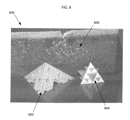
Fig. 6 shows an example 600 of two representative structures 602, 604 next to
foam
606 in which they are to be embedded. The absorber structures 602-604 scatter,
diffract and/or reflect the waves in the dielectric material, e.g., carbon-
based foam or
other type of microwave-absorbing foam. Accordingly, these structures can
allow for
(i.e., provide) greater absorption with a thinner thickness compared to
conventional
absorbers (e.g., prior art wedge absorbers). These structures (e.g., 602-604
as
embedded in 606) can also provide a flat form factor rather than wedge shaped
ones. Such absorbers can be made by suitable techniques, including by use of
3D
printing, such as described in further detail below.
[0040] These absorption systems and components can operate at or across
desired frequency bands. Examples of such frequency bands can include, but are
not limited to, one or more of L, S, C, X, Ku, K Ka, V, and W bands in the
microwave
regime. Attenuation of electromagnetic waves is facilitated via
electromagnetic
-9-
CA 02968375 2017-05-18
WO 2016/081775 PCT/US2015/061690
energy absorbing structures such as shown in Fig. 6 (as 602, 604). Such EM
absorbing structures (or, absorbers) can overcome prior art limitations of
impractical
thickness and limited bandwidth. Use of such EM absorbing structures, e.g.,
602,
604, can provide a method of absorbing that allows a wide bandwidth of
absorption
while maintaining suitable thinness of the absorbers. While exemplary
embodiments
of an absorbing system can be used at radio (RF) frequencies, other
embodiments
can be used at other frequencies, e.g., with appropriate scaling of
structures.
[0041] Exemplary embodiments of EM absorbers can include an absorber that
incorporates fractal structures or features. Such fractal structures or
features can
provide, facilitate and/or enhance the ability to diffuse RF waves. Such
fractal
structures or features may produce additional paths within the absorbing
dielectric
material, thus producing broadband (or, wideband) absorption.
[0042] Any suitable type of dielectric material may be used. An example of
such a
dielectric material can be, but is not limited to, a carbon-based foam. A
commercially
available example of a suitable dielectric foam is C-FOAM PK-2, made available
by
PPG Aerospace Cuming Microwave Corporation of 264 Bodwell Street, Avon, MA
02322 USA; other suitable foams and/or other types of dielectric materials may
be
used instead or in addition. Other examples include suitable microwave-
absorbing
elastomers (elastomeric absorbers) and films, as well as magnetic absorbers.
[0043] In exemplary embodiments, 3D printing using a suitable 3D printer
can be
used to make the structures. Any suitable technique(s) may be used for
embedding
the structures within the dielectric material, e.g., foam. In some
embodiments, an
electromagnetic absorption component, e.g., 602, after being formed by a 3D
printer,
can be placed on a support surface or hung over a support surface while foam
is
poured around it.
[0044] A further aspect of the present disclosure is directed to systems
capable of
producing electromagnetic parts or components¨those that are designed to
propagate, guide, duct, radiate, absorb, reflect, diffract refract, resonate
and/or re-
propagate electromagnetic waves themselves or as components of a larger
system¨and parts made by same. Fig. 7 shows an example 700 of several
components 702-706 after being printed on a 3D printer (not shown).
-10-
CA 02968375 2017-05-18
WO 2016/081775 PCT/US2015/061690
[0045] Such a system can use a three-dimensional (3D) printer to make
volumetric electromagnetic components (or, parts) that incorporate one or more
folds
and/or bends and/or have self-similar structure (e.g., fractal in finite
iterations for at
least a portion of the structure) for at least part of the component. The
component
may be constructed out of conductive plastic or non-conductive plastic or
other non-
conductive material. Alternatively, such systems can use a three-dimensional
printer
to make volumetric metal or metal coated components that incorporate one or
more
folds and/or have self-similar structure (e.g., fractal in finite iterations
for at least a
portion of the structure) for at least part of the component.
[0046] If non-conductive material is used, the component may be plated or
gilded
with a conductor (such as conductive paint) after printing so the component
then
conducts and can act as an electromagnetic component. Alternatively, the
component may only be partially plated and the non-conductive material will
act as a
dielectric. These components may be actual radiators, filters, counterpoises
ground
planes, or loads, absorbers, diffusers, reflectors, directors (lenses),
waveguides, etc.,
and the like. Dipoles, monopoles, dielectric resonators, leaky antennas,
metamaterial
antennas, metasurface antennas, slot antennas, cavity antennas, and many other
kinds of antennas can be made by such systems. The antennas or components may
have smaller size and or better gain and or greater bandwidths than antennas
of
conventional design. They may be used, e.g., from 50-60,000 MHz or any
fraction of
same bandwidth or multiple bands within. They may be used, e.g., in
telematics,
wireless, cell phone communication, WIFI, public safety, Wimax, UWB, and other
systems similar systems.
[0047] Fig. 8 shows an example 800 of EM components 802-816 painted with
conductive paint, after having been printed with a 3D printer. Any suitable 3D
printer
may be used. An example of a suitable 3D printer is the Makerbot Replicator
Fifth
Generation made commercially available by MakerBot' industries, LLC, One
MetroTech Center, 21st Fl, Brooklyn, NY 11201 USA; other suitable 3D printers
may
be used,
[0048] In some implementations/embodiments, an accordioned bicone antenna
apparatus according to an embodiment of the present disclosure can include an
accordioned bicone and a fractalized circuit board, which can be conformal to
a
-11-
CA 02968375 2017-05-18
WO 2016/081775 PCT/US2015/061690
given surface, e.g., a cylinder. The conformal circuit board can be configured
to act
as a fractalized dipole. The circuit board can include one or more conductive
portions or traces that include self-similar structure such as various
suitable fractal
shapes. Such an antenna can be fed by a main feed, which may be configured as
splitting to (i) a bicone feed leading to the center of the accord ioned
bicone, and (ii) a
dipole feed feeding the fractalized dipole section. RLC matching circuitry may
be
used in exemplary embodiments.
[0049]
While the shaping techniques implemented in or for a bicone antenna (or
other shape or configuration of antenna such as disclosed in the patents and
applications incorporated herein) can utilize a folded-shape in the conical
portions
and a fractal shape in/or the conformal portion, other geometric shapes,
including
one or more holes, can be incorporated into the antenna designs. By
incorporating
the folded-shaping into the conical portions, the bicone antenna can provides
the
frequency and beam-pattern performance of a larger sized bicone antenna that
does
not include such shaping.
[0050]
Each folded, e.g., of a bicone portion, can include two faces joined at a
vertex having an included angle of less than 180 degrees as directed away from
a
principal axis of the cone-shaped element and/or antenna. In
exemplary
embodiments, the two faces of a folded do not substantially overlap one
another in a
direction transverse to a bisector of the included angle. For certain
embodiments,
the faces and included angle for a folded can be symmetrical; in other
embodiments,
the faces and includes angle are not symmetrical (e.g., can lie along the two
sides of
a non-Isosceles triangle.)
[0051] The
self-similar shape of the circuit board can be defined as a fractal
geometry. In general, fractal geometry may be grouped into random fractals
(which
can also be referred to as chaotic or Brownian fractals, and include a random
noise
component) or deterministic fractals.
Fractals typically have a statistical self-
similarity at all resolutions and are generated by an infinitely recursive
process. For
example, a so-called Koch fractal may be produced with N iterations (e.g.,
N=1, N=2,
etc.). One or more other types of fractal geometries may also be incorporated
into
the design to produce antenna. Non-fractal portion(s) (such as sawtooth
patterns)
-12-
CA 02968375 2017-05-18
WO 2016/081775 PCT/US2015/061690
can be utilized in conjunction with fractal portion(s). Such patterns can be
utilized,
e.g., as a counterpoise.
[0001] Antenna components can also be made or formed to include
metamaterials. Representative frequencies of operation can include, but are
not
limited to, those over a range of 500 MHz to 1.3 GHz, though others may of
course
be realized. Operation at other frequencies, including for example those of
visible
light, infrared, ultraviolet, and as well as microwave EM radiation, e.g., K,
Ka, X-
bands, etc. may be realized, e.g., by appropriate scaling of dimensions and
selection
of shape of the resonator elements.
[0002] The resonators can be in groups of uniform size and/or configuration
(shape) or of several different sizes and/or geometries. The relative spacing
and
arrangement of groupings (at least one for each specific frequency range) can
be
defined by self-similarity and origin symmetry, where the "origin" arises at
the center
of a structure (or part of the structure) individually designed to have the
wideband
metamaterial property.
[0052] By
incorporating the fractal geometry into the electrically conductive and
non-conductive portions of circuit board, the length and width (e.g., and
consequently, electrical size) of the conductive and non-conductive portions
of the
antenna is increased due to the nature of the fractal pattern. While the
lengths and
widths increase, however, the overall footprint area of circuit board
(fractalized
dipole) is relatively small. By
providing longer conductive paths, dipole (and,
consequently, the related antenna) can perform over a broad frequency band.
[0053] In
exemplary embodiments, matching circuitry/components can be utilized,
e.g., capacitors, RLC circuit(s), etc. Additional tuning can optionally be
augmented/facilitated by placement of tuning elements, e.g., capacitors,
inductors,
and/or RLC circuitry, across the circuit board trace(s), forming a partial
electrical
trap.
[0054]
While certain embodiments have been described herein, it will be
understood by one skilled in the art that the methods, systems, and apparatus
of the
present disclosure may be embodied in other specific forms without departing
from
-13-
CA 02968375 2017-05-18
WO 2016/081775 PCT/US2015/061690
the spirit thereof. Accordingly, the embodiments described herein are to be
considered in all respects as illustrative of the present disclosure and not
restrictive.
-14-