Note: Descriptions are shown in the official language in which they were submitted.
CA 02413714 2002-12-09
File no. 13967-SUS
-1-
TITLE: ADJUSTABLE ELECTRONIC DUPLEXER
FIELD OF THE INVENTION
This invention relates to components for telecommunications devices. More
particularly,
the invention relates to duplexers between transmitters, receivers and
antennas.
BACKGROUND OF THE INVENTION
The duplexer as it is known today gained significance around 1988. Before
then, it was
used for radars in the SOs, 60s and 70s. Some even contained gases. Today ,
the majority
of the duplexers use dielectric materials having a quality factor, which
results in a low
insertion loss. They also use ceramic materials with a high permittivity in
order ~to
miniaturize the passive circuits.
Over the years, the duplexer has evolved as follows:
1953 - Use of duplexers with cav~.ties and in the configuration shown in Fig.
1. The
cavities were in fact band-pass filters, which could be adjusted mechanically.
1956 - The duplexers were made from two hybrids and two tubes. The two tubes
are
filled with gas and play the role of a switch. These duplexers could not send
signals and
receive at the same time; they were therefore "half duplex" applications use
mostly in
military radars. Twenty years later, no major change had been brought to the
duplexers
until the appearance of large cellular systems, which required companies to
research ways
of miniaturizing and optimizing duplexer performance.
1988 - Cellular technology requirements increasingly called for more powerful
and
smaller components. SAW filters (Surface Acoustic Wave) revolutionized this
need.
These filters convert electromagnetic energy into SAW energy. SAW filters
promised to
considerably reduce the volume of the duplexers given that they are very small
and
moreover , they can support higher powers (2 Watts).
CA 02413714 2002-12-09
File no. 13967-SUS
-2-
1995 - Use of SAW filters in GSM cellular band handsets, with the advantage of
a low
insertion loss and a small volume that could be produced in large volumes.
They also
made it possible to avoid the use of traditional components: coils,
capacitors, etc.
1999 - Use of LTCC (Low-Temperature Co-Fired Multilayer Ceramic) technology.
This
technology made it possible to obtain a smaller duplexer. This duplexer used
planar
filters in "stripline" with a high permitivity and a volume of 30% compared to
the cast
solid duplexer, while having the same performance.
2000- Use of two hybrids and two band-stop filters in a chamber filled with
liquid
nitrogen at a temperature of 80 degrees Kelvin thus offering a low insertion
loss by
superconductivity. The two band-stop filters were adjusted to reject the
receiver
frequencies. By using a substrate of LAO (LaAl03), this duplexer gives a loss
by
insertion of less than 1.15 dB and an insulation higher than 35 d.B.
Isolation = SIx_~ = b2~ _ (S2~ ° S2~ + S24 ' S~1 )' e-i4
aia
2001 - The latest technology of duplexers uses FBAR (Miniature Bulk Acoustic
Resonator) technology by Agilent Technologies. This technology makes it
possible for
the duplexer to occupy less than 20% of the volume of conventional ceramic
duplexers.
With the increase in the number of cellular users and the great diversity of
their needs,
mobile communication has never progressed so quickly. 'Thousands of dollars
are
invested in research each year to optimize, miniaturize and find new lower
cost solutions
in order to fill the needs of an extremely profitable market. Most of the
research is
therefore centered on increasingly powerful, small an inexpensive electronic
parts.
Considering the need to miniaturize the handset components, it is normal to
focus on that
which takes the largest volume: the duplexer. The duplexer is fundamentally a
passive
component installed in most full-duplex cellular system. It plays the role of
interface
between the transmitter, the receiver and the antenna. The ultimate objective
of the
duplexer is to convey the power coming from the transmitter towards the
antenna and to
convey the power coming from the antenna towards the receiver. Ideally, no
power must
CA 02413714 2002-12-09
File no. 13967-SUS
-3-
pass between the transmitter and the receiver and vice versa. To meet this
requirement,
the duplexers use analog filters. Thus, in the last twenty years researchers
have
especially concentrated their effort on the discovery of new filter
technologies and not in
the development of various topologies of duplexers.
Thus, there is a need in the industry for better performing and cheaper
duplexers.
SUMMARY OF THE INVENTION
It is an object of the invention to reduce the interference caused by a
leakage signal from
a transmission unit to a reception unit in a communication system or device
sharing an
antenna for transmission and reception.
According to an embodiment, the invention provides a duplexer for a
communication
device having a transmission unit, a reception unit and a shared antenna. The
shared
antenna transmits a portion of a transmission signal provided by the
transmission unit and
receiving a reception signal. The duplexer generates a leakage signal from the
transmission unit toward the reception unit. The leakage signal being added to
the
reception signal. The duplexer comprises a first signal path between the
transmission
unit and the reception unit. The first signal path comprises a filter unit
filtering the
reception signal. The filtering unit provides a filtered signal to the
reception unit. The
duplexer further comprises a second signal path between the transmission unit
and the
reception unit. The second signal path comprises a cancellation unit which
receives a
sample of the transmission signal and produces a compensation signal. The
injection of
the compensation signal to the first signal path substantially reduces the
leakage signal,
thereby producing a substantially leakage-free reception signal.
The cancellation unit may include an attenuator for attenuating the sample of
the
transmission signal to an amplitude substantially equal to the amplitude of
the leakage
signal, and phase-converter for shifting the phase of the transrr~ission
signal substantially
180-degree relative to the phase of the leakage signal.
CA 02413714 2002-12-09
File no. 13967-SUS
-4-
The duplexer may further comprise a third signal path between the first signal
path and
the compensation unit. The third signal path comprises a control unit which
receives a
sample of the substantially leakage-free reception signal and produces the
control voltage
for input to the compensation unit.
According to another embodiment, the invention provides, in a
telecommunication unit
having a shared antenna, a transmission unit and a reception unit, a method
for canceling
the interference generated by the transmission unit in the reception unit. The
method
comprises: acquiring a sample of a transmission signal provided by the
transmission unit;
computing a compensation signal having an amplitude substantially equal to the
amplitude of the leakage signal received by the reception unit and a phase
substantially
180-degree shifted from the phase of the leakage signal received by the
reception unit;
and injecting the compensation signal in the reception unit for substantially
reducing the
leakage signal, thereby producing a substantially leakage-free reception
signal,
According to yet another embodiment, the invention provides, in a
telecommunication
unit having a shared antenna, a transmission unit and a reception unit, a
method for
transmitting a portion of a first signal provided by the transmission unit and
receiving a
second signal using the reception unit. The transmission unit generates a
leakage signal
from the transmission unit toward the reception unit. The leakage signal being
added to
the second signal. The method comprises: transmitting the portion of the first
signal
provided by the transmission unit; acquiring a sample of the first signal
provided by the
transmission unit; computing a compensation signal having an amplitude
substantially
equal to the amplitude of the leakage signal received by the reception unit
and a phase
substantially 180-degree shifted from the phase of the leakage signal received
by the
reception unit; receiving the second signal; and injecting the compensation
signal into the
second signal for substantially reducing the leakage signal, thereby producing
a
substantially leakage-free reception signal.
CA 02413714 2002-12-09
File no. 13967-SUS
-5-
BRIEF DESCRIPTION OF THE DRAWINGS
FIG. 1 is a block diagram of a conventional prior art duplexer;
FIG. 2 is a block diagram of another conventional prior art duplexer;
FIG. 3 is a block diagram of a communication system comprising a duplexer
built in
accordance with an embodiment of the invention;
FIG. 4 is a chart showing the amplitude and phase mismatch requirements to
achieve
various suppression levels of the signal transmitted from the transmitter to
the receiver;
FIG. 5 is a block diagram of an ideal suppression circuit used for computer
simulations;
FIG. 6A and 6B are charts showing exemplary parameters of a YIG filter used in
an
embodiment of the invention; and
FIG. 7 is a block diagram of a communication system comprising a duplexer
built in
accordance with another embodiment of the invention.
DESCRIPTION OF THE PREFERRED EMBODIMENTS OF THE INVENTION
Today's standard duplexer 10 is shown in Fig. 1. It is a passive RF component
with three
ports: a transmitter port 14, a receiver port 16 and the antenna port 12. Two
band-pass
filters 18 and 20 are necessary in order to isolate the transmitter port 14
and the receiver
port 16. In theory, no power coming from the transmitter 14 port must pass
through to
the receive port 16. The frequency of the transmitter is offset from that of
the receiver.
Another type of duplexer 20 is shown in Fig. 2. Duplexer 22 uses two hybrids
32 and 34
and two band-stop filters 36 and 38 in a chamber filled with liquid nitrogen
at a
temperature of 80 degrees Kelvin thus offering a low insertion loss by
superconductivity.
Duplexer 22 also includes a transmitter port 24, a receiver port 26, an
antenna port 30,
and a match load port 28. The two band-stop filters 36 and 38 are adjusted to
reject the
receiver frequencies. By using a substrate of LAO (LaAlO,), this duplexer
gives an
insertion loss of less than 1.15 dB and an insulation greater than 35 dB.
CA 02413714 2002-12-09
File no. 13967-SUS
-6-
An ideal duplexer has the following characteristics: infinite return loss at
each port
(transmitter, receiver, and antenna); no transmission loss between the Tx port
and the
antenna port; no transmission loss between the antenna port and the receiver
port; and
complete insulation between the Tx port and the Rx port.
It is important to define the following terms:
"Insertion Loss Tx-Ant" is the loss in dB between the Tx port and the antenna
port.
"Insertion Loss Ant-Rx" is the loss in dB between the antenna port and the Rx
port.
"Insulation" is the ratio of power in dB which is propagated from the Tx port
to the Rx
port as well as from the Rx port to the Tx port.
"Tx band" is the frequency band, which is less than 3 dB down when compared to
the
peak of the Tx-Ant transmission curve.
"Rx band" is the frequency band, which is less than 3 dB down when compared to
the
peak of the Ant-Rx transmission curve.
"Maximum Power" is the power in dBm or Watts, which the Tx port of the
duplexer can
support towards the antenna.
"SWR or Return Loss" corresponds to the rate of adaptation. of the impedance
of the
ports.
"Ripple" is the variation of undulation in dB on the Tx or Rx band of
operation.
"Leakage signal" is the difference between the transmission signal provided by
tlae
transmission unit and the portion of the transmission signal transmitted by
the antenna.
All of today's miniature duplexers offer low insulation (in the order of 30
dB) and the
frequency bands allocated to the transmitter and receiver are fixed. Duplexers
with
cavities offer low insertion loss and have excellent insulation in the order
of 80 dB or
more. On the other hand, these dup:lexers are large and must be adjusted
mechanically.
In order to deal with these problem, a new topology the new topology shown in
the
exemplary embodiment of Fig. 3. The new topology adds a feed forward loop to
the
standard duplexer 10 of Fig. 1 to produce duplexer 40.
CA 02413714 2002-12-09
File no. 13967-SUS
-7_
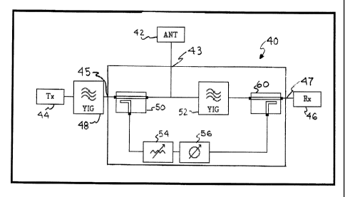
Duplexer 40 has a transmitter port 45, a receiver port 47 and an antenna port
43.
Duplexer 40 shown in Fig. 3 only has one YIG filter 52. An additional YIG
filter is
shown at the input of the duplexer 40. A "YIG filter" is a band-pass filter
controlled by a
power source and has a very wide frequency range. A YIG filter is relatively
cheap.
Unfortunately, the insertion loss of a YIG filter is relatively high, i.e.,
approximately 3 to
6 dB.
The use of directional couplers 50 and 60, an attenuator 54 and phase-
converter 56 makes
it possible to increase the insulation between transmitter 44 and receiver 46.
Antenna 42
is also shown in Fig. 3. The lower loop (second signal path) samples the
transmitter
signal through a coupler 50, attenuates it (with attenuator 54) to the same
power as the
signal on the output side of the YICT filter 52, phase reverses it (with phase-
converter 56)
to obtain 180 degrees difference between the two signals. The lower loop
therefore
produces a compensation signal. T'he compensation signal is then injection in
the upper
loop (the first signal path) through coupler 60. In an ideal duplexer the
leakage signal
would be completely removed at the Rx port 47.
In order to remove the leakage signal, it is important to understand some
theory about
how to increase insulation by tens of dBs.
~A(dB) ~,4(dB)
R(dB) =10 ~ log 10 '° + 1- 2 ~ 10 Z° ~ cos(~)
where 0A is the difference in amplitude between the two signals in dB
R(dB) is the level of suppression
cp is the difference in phase between the two signals expressed in degrees
To obtain perfect suppression, three conditions are needed:
1- The amplitudes must be equal;
2- The two signals must be 180 degrees out-of phase; and
3- The two signals must have the same propagation delay.
CA 02413714 2002-12-09
File no. 13967-SUS
_g_
Persons skilled in the art will understand that a high degree of accuracy is
required in
order to obtain high levels of supprc;ssion. Fig. 4 shows various suppression
level curves
and the phase mismatch and amplitude mismatch requirements to obtain each
suppression
level. Shown suppression levels are as follows: 25 dB on curve 62; 30 dB on
curve 64,
40 dB on curve 66, 80 dB on curve 58 and 90 dB on curve 70. In an example, to
reach a
suppression level of 40 dB (curve 66), it is necessary that the difference in
amplitude be
equal to 0.06 dB and of 0.4 degrees between the two signals. Suppression
levels of 80 dB
or more (curves 68 and 70) would be interesting, but the required precision is
difficult to
achieve in practice. Considering that a signal is never repetitive (a CDMA
modulated
signal, for example), propagation delay of the two signal of the two paths
should be as
close to equal as possible (substantially equal). If this condition is not
met, good
suppression will not be achieved for the simple reason that the signals will
be out-of
phase at receiver 46.
The simulation circuit 72 shown i:r~ Fig. 5 was used in order to demonstrate
the feed
forward principle and the ability to use the duplexer 40 in the 1.7 GHz to
2GHz range. A
50 dB attenuator 76 plays the role of a band-pass filter. The signal coming
from port 1
will be attenuated by 50 dB in the upper path, without any phase variation.
There is no
additional loss since the couplers 74 and 78 are ideal, thereby presenting
zero insertion
loss. Given that the couplers 74 and 78 offer a coupling coefficient of 10 dB
without any
change in phase, the signal traveling on the lower path will be attenuated by
50 dB by
attenuator 80, and be subjected t:o a 180 degree phase shift (by phase-shifter
82)
compared to the signal on the upper loop. The superposition of two the upper
and lower
loop signal by coupler 78 will result in suppression of the undesirable signal
(leakage
signal) from port 75. Figs. 6A and EiB show characteristics for an exemplary
YIG filter.
In order to maximize removal of the undesirable Tx signal (leakage signal) to
the port 79,
it is necessary to work in a zone that is stable in phase and amplitude. YIG
filters
normally have a weak return loss at their resonance frequency which results in
a good
level of insertion loss. As shown in Fig. 6A (curves 84 and 86), the stable
zone is around
CA 02413714 2002-12-09
File no. 13967-SUS
-9-
1.75 GHz. As shown in Fig. 6B (curve 88 and 90), the exemplary YIG filter has
a low
return loss at its resonance frequency (around 1.9 GHz) thereby providing good
insertion
loss.
Persons skilled in the art will know that attenuator and phase converter
characteristics
vary with their input voltages. Also, attenuator and phase converter
characteristics may
not be constant over a given operating frequency range (e.g., 1.7 GHz to 2.0
GHz). It
may therefore be required to successively adjust attenuator and phase
converter voltages
to obtain maximum suppression.
Another embodiment could therefore include automated control of attenuator and
phase-
converter voltages as shown in Fig. 7. In this embodiment, an automated
control unit 1 l2
is placed at the output of the duplexer 92. The coupled signal (using coupler
110) is
analyzed by, for example, a crystal detector. RF power is then converted to DC
voltage
in the control unit 112. Control unit 112 then optimizes the attenuator 104
and the phase-
converter 106 in accordance with t:he previously obtained DC voltage. The
remaining
components in Fig. 7 (antenna 94, transmitter unit 96, receiver unit 98,
couplers 100 an
108, and filter 102) are similar to those described in Fig. 3.
In yet another embodiment, the phase-converter 106 has phase correction
capabilities that
are optimized for each frequency in the frequency of interest.
One of the possible applications for the technology described herein is the
MMIC cellular
technology. All passive components described herein can easily be made on a
large scale
basis.
The invention may be embodied in other specific forms without departing from
its spirit
or essential characteristics. The described embodiments are to be considered
in all
respects only as illustrative and not restrictive and the scope of the
invention is, therefore,
indicated by the appended claims rather than the foregoing description. All
changes
CA 02413714 2002-12-09
File no. 13967-SUS
-10-
which come within the meaning and range of equivalency of the claims are to be
embraced within their scope.