Note: Descriptions are shown in the official language in which they were submitted.
CA 02997524 2018-03-02
WO 2017/045071
PCT/CA2016/051079
1
POWER CONVERTER CONFIGURED FOR LIMITING SWITCHING
OVERVOLTAGE
TECHNICAL FIELD
[0001] The present disclosure relates to the field of power electronics.
More specifically, the present disclosure relates to a power converter
configured
for limiting switching overvoltage
BACKGROUND
[0002] Commutation cells are commonly used in electronic systems that
require conversion of a voltage source, including both DC-DC converters and DC-
AC converters, which are often called inverters. With the limited space
allowed for
power converter circuits, such as those used for example in electric and/or
electric
hybrid automotive applications, and given the high cost of the semi-
conductors,
the demand for integration of these commutation cells increases.
[0003] A known way of reducing the space occupied by semiconductors
in power converter circuits is to increase their efficiency to allow the size
of the
cooling surface to be reduced.
[0004] Losses in power electronic switches present in conventional
power converter circuits are mainly caused by two sources; conduction losses
and
switching losses. One way to reduce switching losses is generally by
accelerating
turn-on and turn-off of the power electronic switches. However, fast turn-off
of the
power electronic switches induces overvoltage in stray inductances of their
high-
frequency loop. It is thus often required to slow down turning off of the
power
electronic switches to protect them against overvoltage. This may seriously
impact
the overall efficiency of conventional power converter circuits.
CA 02997524 2018-03-02
WO 2017/045071
PCT/CA2016/051079
2
[0005] Figure 1 is an idealized circuit diagram of a conventional
commutation cell such as those used in conventional power converter circuits.
A
commutation cell 10 converts a DC voltage Vbõ from a voltage source 12 (or
from
a capacitor) into a current source 'out (or into an inductance) that usually
generates a voltage Võt appropriate for a load 14 connected to a positive tab
of
the voltage source 12, the load 14 being for example a resistive load, an
electric
motor, and the like. The commutation cell 10 comprises a freewheel diode 16
and
a controlled power electronic switch 18, for example an isolated gate bipolar
transistor (IGBT). A capacitor 20 (Cm) is used to limit variations of the
voltage Vbõ
of the voltage source 12 and an inductance Lõt 32 is used to limit the
variations of
the output current Iõt. A gate driver (not shown in Figure 1 but shown on
later
Figures) controls turning on and off of the power electronic switch 18. Figure
1
illustrates a configuration of the commutation cell 10, of the load 14, and of
the
voltage source 12, in which energy flows from the voltage source 12 to the
load
14, i.e. from left to right on the drawing. The commutation cell 10 can also
be used
in a reverse configuration in which energy flows in the opposite direction, in
which
case the load 14 is connected between the output inductance Lõt 32 and a
negative tab of the voltage source 12.
[0006] When turned on (i.e. closing), the power electronic switch 18
allows current to pass therethrough, from its collector 22 to its emitter 24;
at that
time, the power electronic switch 18 can be approximated as a closed circuit.
When turned off (i.e. opening), the power electronic switch 18 does not allow
current to pass therethrough and becomes an open circuit.
[0007] The gate driver applies a variable control voltage between the
gate 26 and the emitter 24 of the power electronic switch 18. For some types
of
power electronic switches such as bipolar transistors, the gate driver may act
as a
current source instead of as a voltage source. Generally, when the voltage
CA 02997524 2018-03-02
WO 2017/045071
PCT/CA2016/051079
3
applied between the gate 26 and the emitter 24 is "high", the power electronic
switch 18 allows passing of current from the collector 22 to the emitter 24.
When
the voltage applied between the gate 26 and the emitter 24 is "low", the power
electronic switch 18 blocks passage of current therethrough. In more details,
a
voltage difference between the gate 26 and the emitter 24, denoted Vge, is
controlled by the gate driver. When Vge is greater than a threshold Vge(th)
for the
power electronic switch 18, the switch 18 is turned on and a voltage Võ
between
the collector 22 and the emitter 24 becomes near zero. When Vge is lower than
Vge(th), the power electronic switch 18 is turned off and Võ eventually
reaches
Vbus=
[0008] When the power electronic switch 18 is turned on, a current lout
flows from the voltage source 12 (and transiently from the capacitor 20)
through
the load 14 and through the collector 22 and the emitter 24. When the power
electronic switch 18 is turned off, the current lout circulates from the load
14 and
passes in the freewheel diode 16. It may thus be observed that the power
electronic switch 18 and the freewheel diode 16 operate in tandem. Turning on
and off of the power electronic switch 18 at a high frequency allows the
current
lout, in the output inductance Lout 32, to remain fairly constant.
[0009] It should be observed that, in the case of other power electronic
switch types, for example bipolar transistors, the term "gate" may be replaced
with
"base", the base being controlled by a current as opposed to the gate that is
controlled by a voltage. These distinctions, well known to those skilled in
the art,
do not change the overall operation principles of the commutation cell 10.
[0010] Figure 2 is another circuit diagram of the conventional
commutation cell of Figure 1, showing parasitic (stray) inductances. In
contrast
with the idealized model of Figure 1, connections between components of an
actual commutation cell define parasitic inductances. Though the parasitic
CA 02997524 2018-03-02
WO 2017/045071
PCT/CA2016/051079
4
inductances are distributed at various places within the commutation cell 10,
a
suitable model presented in Figure 2 shows two (2) distinct inductances
representing the overall parasitic inductance, including an emitter inductance
30
of the power electronic switch 18 and an inductance 34 representative of all
other
parasitic inductances (other than the emitter inductance 30) around a high
frequency loop 36 formed by the freewheel diode 16, the power electronic
switch
18 and the capacitor 20. The high frequency loop 36 is a path where current
changes significantly upon switching of the power electronic switch 18. It
should
be noted that an output inductance Lõt 32 is not part of the high frequency
loop
36 because its current remains fairly constant through the commutation period.
[0011] Figure 3 is a circuit diagram of a conventional commutation cell
further showing a gate driver 40. Some elements of the commutation cell 10 are
not shown on Figure 3, in order to simplify the illustration. Figure 3 shows a
gate
driver 40 having a positive supply voltage 42, a negative supply voltage 44
and an
output 46 being connected to the gate 26 of the power electronic switch 18 via
a
gate resistor Rg. The positive supply voltage 42 of the gate driver 40 has a
value
denoted +Võ, for example +15 volts above a ground reference (shown on a later
Figure) while the negative supply voltage 44 has value denoted -Vdd, for
example
-5 volts below the ground reference. A ground reference of the gate driver 40
is
connected to the emitter 24 of the power electronic switch 18; this connection
is
not shown on Figure 3. An input 50 of the gate driver 40 is connected to a
controller (not shown) of the commutation cell 10, as is well known in the
art. A
voltage at the output 46 of the gate driver 40 goes up to +Võ and goes down to
-
Vdd in order to control the voltage at the gate 26. The input resistance of
the gate
26 to emitter may be very high, especially in the case where the electronic
switch
18 is an IGBT. However, a parasitic capacitance Cge (shown on a later Figure),
present between the gate 26 and the emitter 24 and a parasitic Miller
capacitance
CA 02997524 2018-03-02
WO 2017/045071
PCT/CA2016/051079
Cgc (not shown), present between the gate 26 and the collector 22, for a total
gate
equivalent capacitor Cies, causes some current to flow from the output 46 when
the gate driver 40 alternates between +Võ and -Vdd. The value Rg of the gate
resistor is selected as a function of the parasitic capacitance Cies and of a
desired
switching rate of the power electronic switch 18 so that the voltage at the
gate 26
changes at a rate appropriate for the desired switching rate.
[0012] On Figure 3, a current /jot flowing through the power electronic
switch 18 and through the emitter parasitic inductance 30 is essentially equal
to
'out when the power electronic switch 18 is closed, and quickly reduces to
substantially zero when the power electronic switch 18 turns off.
[0013] When the power electronic switch 18 turns on or off, the current
Lgbt flowing therethrough increases or diminishes at a fast rate. These
variations of
Lgbt, denoted di/dt, induce voltage across inductances 30 and 34, according to
the
well-known equation (1):
di
= L = ¨dt (1)
[0014] wherein VL is a voltage induced across an inductance and L is an
inductance value.
[0015] A voltage VL, is induced across the parasitic inductance 34 and
a
voltage VL, is induced across the emitter parasitic inductance 30. On Figures
2
and 3, the polarities shown across the inductances of the high frequency loop
36,
including the emitter inductance 30, reflect voltages obtained upon turn-off
of the
power electronic switch 18, when the /jot current diminishes very rapidly,
di/dt
thus taking a negative value. Upon turn-on of the power electronic switch 18,
voltages across the inductances of the high frequency loop 36, including the
emitter inductance 30, are in the opposite direction.
CA 02997524 2018-03-02
WO 2017/045071
PCT/CA2016/051079
6
[0016] These voltages VL, and I/Le are in series with Vbõ from the
voltage source 12. When the power electronic switch 18 turns off, the
collector 22
to emitter 24 voltage increases until the freewheel diode 16 turns on. At that
time,
addition of Vbus, VLs and I/Le results in an important overvoltage applied
between
the collector 22 and the emitter 24 of the power electronic switch 18. Though
power electronic switches are rated for operation at some level of
overvoltage,
extreme overvoltage can reduce the lifetime of any power electronic switch to
thereby lead to its premature failure.
[0017] Figure 4 is a circuit diagram of an IGBT leg having resistive
dividers connected across parasitic (stray) emitter inductances, forming
compensation circuits. The circuit of Figure 4 was introduced in International
Patent Publication No. WO 2014/161080 A1 to Jean-Marc Cyr et al., published on
October 9, 2014, the disclosure of which is incorporated by reference herein.
[0018] Generally, Figure 4 shows a power converter having a pair of
commutation cells connected in parallel, each commutation cell including a
power
electronic switch and a gate driver. The power converter may for example be an
IGBT leg 90 including compensation circuits connected to gate drivers in a
configuration that reduces overvoltage on the IGBTs. The IGBT leg 90 may for
example form one third of a three-phase alternative current (AC) power source
driving an electric motor (not shown) from battery 12. The IGBT leg 90 feeds a
current source lout via an inductance Lut through a phase tab (not shown)
connected between top and bottom power electronic switches, the phase tab
having a parasitic inductance Lphase= Figure 4 introduces compensation
circuits
that optimize overvoltage on the IGBT using a resistive divider across the
emitter
parasitic inductance.
[0019] The IGBT leg 90 comprises a top commutation cell including a top
IGBT Q2 and a bottom freewheel diode D1. The top IGBT Q2 is driven by a gate
CA 02997524 2018-03-02
WO 2017/045071
PCT/CA2016/051079
7
driver 62 connected to a gate 64 of the top IGBT Q2 via a resistor R4. A top
compensation circuit includes a turn-on diode D4 and resistors R5 and R6. In
the
IGBT leg 90, a bottom commutation cell includes a bottom IGBT Qi and a top
freewheel diode D2. The bottom IGBT Qi is driven by a gate driver 60 connected
to a gate 26 of the bottom IGBT Q1 via a resistor R1. A bottom compensation
circuit includes a turn-on diode D3 and resistors R2 and R3. The top
commutation
cell operates when lout is positive (in the direction shown in Figure 4) and
the
bottom commutation cell operates when lout is in the opposite direction.
[0020] Components of the IGBT leg 90 are placed on a power module
(not shown) having a positive voltage tab connected to + Vbõ, a negative
voltage
tab connected to -Vbõ (also not shown) and a phase voltage tab connected to
Lõt.
Connections between these components create a number of parasitic
inductances, including a parasitic positive voltage tab L-Fvbõ, a parasitic
top
collector inductance Lc-high, a parasitic top emitter inductance Le-high, a
parasitic
bottom collector inductance Lc40w, a parasitic bottom emitter inductance
Le_ibw, a
parasitic negative voltage tab inductance L_vbõ and input capacitor inductance
L.
The two commutation cells combine with an input capacitance C,, of a voltage
source 12 to form a high frequency loop 92 of the IGBT leg 90.
[0021] Discussing the bottom commutation cell of the IGBT leg 90 of
Figure 4, the gate 26 of the bottom IGBT Qi connected to its gate driver 60
via the
resistor R. A ground reference 52 of the gate driver 60 (GND low) is connected
to
a bottom compensation circuit having a resistive divider circuit including the
two
resistors R2 and R3 and the turn-on diode D3, which allows the turn-on not to
be
impacted by the resistive divider by keeping the voltage at the emitter of the
bottom IGBT Qi not lower than the ground reference 52. The turn-on diode D3 is
conducting while turning on the bottom IGBT Qi because the direction of its
current in positive. In contrast, the turn-on diode D3 is not conducting while
turning
CA 02997524 2018-03-02
WO 2017/045071
PCT/CA2016/051079
8
off the bottom IGBT Q1 because of the voltage induced across the emitter
inductance during the di/dt applies a negative voltage across the turn-on
diode D3.
[0022] In the circuit of Figure 4, values of the resistors R2 and R3
are
selected according to an acceptable overvoltage level allowed across the
bottom
IGBT Q1. A ratio of R2 over R3 is increased to reduce the overvoltage. The
value
of the equivalent gate resistor is set with these two resistors R2 and R3 in
parallel,
in series with a gate driver resistor R1. A value of the gate driver resistor
R1 is
adjusted in a conventional manner according to a proper commutation behavior.
[0023] In other words, the normal practice consisting in using a
resistor
R1 in the ground connection of the gate driver to limit the current in the
diodes that
protect the gate driver 60 of the bottom IGBT Qi from a negative voltage when
the
top IGBT Q2 turns off has been modified by splitting the resistor in two
resistors,
including R1 in series with R2 and R3 connected in parallel, and by adapting
their
ratio to limit the effect of the emitter inductance on the di/dt. An
equivalent resistor
value may remain the same, but the voltage divider gives the desired weight of
the emitter inductance to limit the overvoltage at the desired level.
[0024] By correctly setting values of the resistors of the compensation
circuits, it is possible to reduce the effect of the emitter inductance to get
the
maximum overvoltage allowed to therefore improve the efficiency.
[0025] The overvoltage can be optimized as much as possible to reach
the maximum IGBT rating while maintaining the speed of the di/dt for
efficiency
reasons. This is done by reducing a value of R2, the resistor connected to the
IGBT emitter, compared to R3, the resistor connected to the power tab. The
voltage across the emitter inductance is thus split in two parts and only the
part of
the voltage across R2 is applied in the gate drive circuit to limit the gate
voltage
drop.
CA 02997524 2018-03-02
WO 2017/045071
PCT/CA2016/051079
9
[0026] The values of the resistors R2 and R3 are selected according to
the level of overvoltage allowed across Q1. Figure 5 is a diagram showing turn-
off
waveforms of the bottom IGBT of Figure 4. In more details, Figure 5 show the
result of a resistive divider optimized for an operation at a bus voltage Vbõ
of 500
Vdc. The ratio of R2 over R3 can be increased to reduce the overvoltage. The
equivalent value of the two resistors R2 and R3, in parallel, is set in series
with R1,
which is adjusted according to the proper commutation behavior of the bottom
IGBT Qi. By setting the resistor values correctly, it is possible to reduce
the effect
of the emitter inductance to get the maximum overvoltage allowed on the bottom
IGBT Qi to therefore improve the efficiency.
[0027] The collector to emitter overvoltage may be optimized as much as
possible to reach the maximum voltage rating of the bottom IGBT Qi. This is
done
by reducing a value of the resistor R2 connected to the logical emitter of the
bottom IGBT Qi compared to a value of the resistor R3 connected to the power
tab. The voltage across the emitter inductance Le_iow, alone or with the
negative
voltage tab inductance L_vbõ, is split in two parts and only the voltage
across the
resistor R2 is applied at the reference 52 of the gate driver 60 to limit the
voltage
drop at the gate 26 of the bottom IGBT Qi.
[0028] Figure 5 shows the current Lgbt, the gate to emitter voltage Vge
and the collector to emitter voltage Võ during turn-off of the bottom IGBT Qi
of
Figure 4. It is notable that Võ peaks at a plateau 80 whose value is tailored
according to the maximum voltage rating of the bottom IGBT Qi. This plateau 80
occurs while the rate of drop of Vge is contained at area 82 by the insertion
of the
voltage sample from the parasitic inductances Le-low and L-Vbus=
[0029] Figure 6 is a circuit diagram in which the compensation circuits
of
Figure 4 are modified to impact the turn-on of the IGBTs. A variant of the
circuit of
Figure 6 was introduced in US Provisional Patent Application serial number
CA 02997524 2018-03-02
WO 2017/045071
PCT/CA2016/051079
62/183,437 to Jean-Marc Cyr et al., filed on June 23, 2015, the disclosure of
which is incorporated by reference herein.
[0030] Generally, Figure 6 shows a modified IGBT leg 95 in which the
ground reference 52 (GND low) is now electrically connected to the emitter 24
of
the bottom IGBT Q1 via the turn-on diode D3 placed in series with a resistor
RD3.
The turn-on diode D3 is polarized to become short when an emitter voltage of
the
bottom IGBT Qi is higher than a voltage of the ground reference 52. The ground
reference 52 is also electrically connected across both parasitic inductances
Le_k,,
and L-Vbus via the resistor R2 and R3. The resistor R2 is placed in parallel
with the
series combination of the turn-on diode D3 and of the resistor RD3. If the
resistor
RD3 is replaced by a short circuit, there is no compensation at turn-on and
the
IGBT leg 95 becomes equivalent to the IGBT leg 90, at least for the bottom
compensation circuit. In the presence of the turn-on diode D3, selection of a
proper value for the resistor RD3 allows to fine tune the turn-on of the
bottom IGBT
Qi independently from its turn-off, the bottom compensation circuit forming a
resistive divider between RD3 in parallel with R2, this parallel combination
being in
series with R3.
[0031] A ground reference 54 (GND high) is electrically connected to the
emitter of the top IGBT Q2, via the turn-on diode D4 placed in series with a
resistor
RD4. Turn-on diode D4 is polarized to become short when an emitter voltage of
the
top IGBT Q2 is higher than a voltage of the ground reference 54. The ground
reference 54 is also electrically connected to collector 22 of the bottom IGBT
Qi
via the resistor R6. The resistor R6 is placed in parallel with the series
combination
of the turn-on diode D4 and of the resistor RD4. In the presence of the turn-
on
diode D4, selection of a proper value for the resistor RD4 allows to fine tune
the
turn-on of the top IGBT Q2 independently from its turn-off, the top
compensation
circuit forming a resistive divider between RD4 in parallel with R6, this
parallel
CA 02997524 2018-03-02
WO 2017/045071
PCT/CA2016/051079
11
combination being in series with R6.
[0032] Considering the IGBT leg 90 of Figure 4 and the IGBT leg 95 of
Figure 6, the top and bottom compensation circuits operate in similar ways.
However, in a typical implementation, the emitter inductance Le-high of the
top
IGBT Q2 is smaller than the emitter inductance Le-low of the bottom IGBT Q1.
Though the collector inductance Liow of the bottom IGBT Qi can be combined
with the emitter inductance Le-high of the top IGBT Q2, Figures 4 and 6
showing
that the resistor R6 is connected between the emitter inductance Le-high of
the top
IGBT Q2 and the collector inductance Lc_iow of the bottom IGBT Q1, this
combination is still smaller than the combination of the negative voltage tab
inductance L_vbõ with the emitter inductance Le_iow. For that reason, though
the top
and bottom commutation cells of the IGBT legs 90 and 95 are constructed in the
same manner, their behavior is somewhat different. While the above-described
techniques work very well for the bottom IGBT Qi, the emitter inductance Le-
high is
often too small to suitably clamp a voltage thereacross without increasing the
gate
resistor R4 to protect the device. In fact, in practice, the emitter
inductance Le-high
of the top IGBT Q2 in series with the collector inductance Lc_iow of the
bottom IGBT
Qi , is oftentimes too low to be used to limit the overvoltage across the top
IGBT
Q2 at the desired level.
[0033] Therefore, there is a need for improvements in circuits capable
of
reducing overvoltage occurring upon switching in a power converter.
SUMMARY
[0034] According to the present disclosure, there is provided a power
converter configured for limiting switching overvoltage. The power converter
comprises a bottom commutation cell that includes a bottom power electronic
switch having a bottom gate, a bottom gate driver and a bottom compensation
CA 02997524 2018-03-02
WO 2017/045071
PCT/CA2016/051079
12
circuit connected to a bottom parasitic inductance. The bottom compensation
circuit applies a sample of a voltage induced across the bottom parasitic
inductance to the bottom gate driver at turn-off of the bottom power
electronic
switch. The power converter also comprises a top commutation cell that
includes
top power electronic switch having a top gate, a top gate driver and a top
compensation circuit connected to the bottom parasitic inductance. The top
compensation circuit applies a sample of a voltage induced across the bottom
parasitic inductance to the top gate driver at turn-off of the top power
electronic
switch. The top and bottom commutation cells are part of a loop, being
connected
at a junction of a collector of the bottom power electronic switch and of an
emitter
of the top power electronic switch.
[0035] The foregoing and other features will become more apparent
upon reading of the following non-restrictive description of illustrative
embodiments thereof, given by way of example only with reference to the
accompanying drawings.
BRIEF DESCRIPTION OF THE DRAWINGS
[0036] Embodiments of the disclosure will be described by way of
example only with reference to the accompanying drawings, in which:
[0037] Figure 1 is an idealized circuit diagram of a conventional
commutation cell such as those used in conventional power
converter circuits;
[0038] Figure 2 is another circuit diagram of the conventional
commutation cell of Figure 1, showing parasitic (stray)
inductances;
[0039] Figure 3 is a circuit diagram of a conventional commutation cell
CA 02997524 2018-03-02
WO 2017/045071
PCT/CA2016/051079
13
further showing a gate driver;
[0040] Figure 4 is a circuit diagram of an IGBT leg having resistive
dividers connected across parasitic (stray) emitter inductances,
forming compensation circuits;
[0041] Figure 5 is a diagram showing turn-off waveforms of the bottom
IGBT of Figure 4;
[0042] Figure 6 is a circuit diagram in which the compensation circuits
of
Figure 4 are modified to impact the turn-on of the IGBTs; and
[0043] Figure 7 is a circuit diagram of an IGBT leg having turn-off
diodes
mounted in tandem according to an embodiment.
[0044] Like numerals represent like features on the various drawings.
DETAILED DESCRIPTION
[0045] Various aspects of the present disclosure generally address one
or more of the problems related to overvoltage occurring upon switching in a
power converter.
[0046] Circuits operable to limit overvoltage in commutation cells,
especially at turn-off of IGBTs, are described in international patent
publications
no WO 2013/082705 A1, WO 2014/043795 A1, WO 2014/161080 A1, WO
2015/061901 A1, WO 2015/070347 A1 and WO 2015/139132 A1 and in US
provisional application no 62/183,437, all of which are authored by Jean-Marc
Cyr
et al. the disclosure of these being incorporated by reference herein. The
present
technology provides control of overvoltage and switching losses at turn-off of
a
power electronic switch of a commutation cell. Circuits and methods presented
herein are generally compatible with at least some aspects these other
solutions
to limit overvoltage at turn-off of power electronic switches.
CA 02997524 2018-03-02
WO 2017/045071
PCT/CA2016/051079
14
[0047] In a commutation cell, di/dt at turn-off of a power electronic
switch
induces a voltage across parasitic (stray) inductances of a high frequency
loop of
the commutation cell. This voltage is present across the power electronic
switch in
addition to a bus voltage providing power to the commutation cell. A sum of
these
voltages can exceed the maximum voltage rating of the power electronic switch.
Solution described hereinabove are based on the application of a sample of the
overvoltage present across parasitic inductances of the commutation cell to a
gate
driver of the power electronic switch. When a pair of power electronic
switches is
connected in series to form a leg, because of circuit configurations that are
generally used in such legs, a parasitic inductance present in a "top"
commutation
cell may not be sufficient to provide a sufficient voltage sample to control
the
overvoltage present across the top power electronic switch. An improvement
described in details hereinbelow comprises a compensation circuit that is
configured to sample a voltage induced across a parasitic inductance of one
commutation cell to control the overvoltage upon turn-off of the other
commutation
cell. According to this solution, voltage samples are taken in the commutation
cell
having the largest parasitic inductance and are applied at turn-off of both
commutation cells.
[0048] The techniques disclosed herein will mainly be described in
relation to the use of isolated gate bipolar transistors (IGBT). Mentions of
IGBTs in
the following description are made for illustration purposes and are not meant
to
limit the present disclosure. The same techniques may equally be applied to
commutation cells constructed using metal¨oxide¨semiconductor field-effect
transistors (MOSFET), bipolar transistors and like power electronic switches.
[0049] The following terminology is used throughout the present
disclosure:
[0050] Commutation cell: an assembly of electronic components
CA 02997524 2018-03-02
WO 2017/045071
PCT/CA2016/051079
connected to a voltage source that alternatively applies voltage
from a voltage source and zero voltage to a current source
connected to a load.
[0051] Power converter: circuit configured to convert energy from a
first
type of energy source, providing a different type of energy.
[0052] Leg: a combination of a pair of commutation cells forming a power
converter.
[0053] Overvoltage: voltage across an electronic element that exceeds
the voltage from the power source.
[0054] Power electronic switch: an active on and off switchable element
of a commutation cell.
[0055] Bottom, top: in the context of the present disclosure, the terms
"top" and "bottom" do not relate to physical characteristics of any
element of the power converter, but rather to their placement on
circuits diagrams shown in the various drawings.
[0056] Compensation circuit: a circuit configured to provide a measure
of
the overvoltage on a power electronic switch as feedback to
control and/or reduce the overvoltage.
[0057] Parasitic inductance: an inductance that is usually not formed of
a
discrete component, but rather formed by the connection of two or
more components such as the connection between a power
electronic switch and a circuit board; also called stray inductance.
[0058] Voltage sample: a voltage obtained from a circuit component, for
example from a parasitic inductance, the obtained voltage being
reduced by a voltage gain.
CA 02997524 2018-03-02
WO 2017/045071
PCT/CA2016/051079
16
[0059] Resistive gain adapter: a combination of resistors providing a
voltage gain.
[0060] Turn-on diode: a diode of a compensation circuit that is
conductive during the turn-on of the power electronic switch in
that compensation circuit.
[0061] Turn-off diode: a diode of a compensation circuit that is
conductive during turn-off of the power electronic switch in that
compensation circuit.
[0062] Freewheel diode: a diode in an anti-parallel position having
regard to a power electronic switch.
[0063] Gate driver: a small buffer amplifier providing isolation and
control
signals for turning on and off a power electronic switch.
[0064] Reference: a floating ground reference of a gate driver on which
a
voltage sample can be applied.
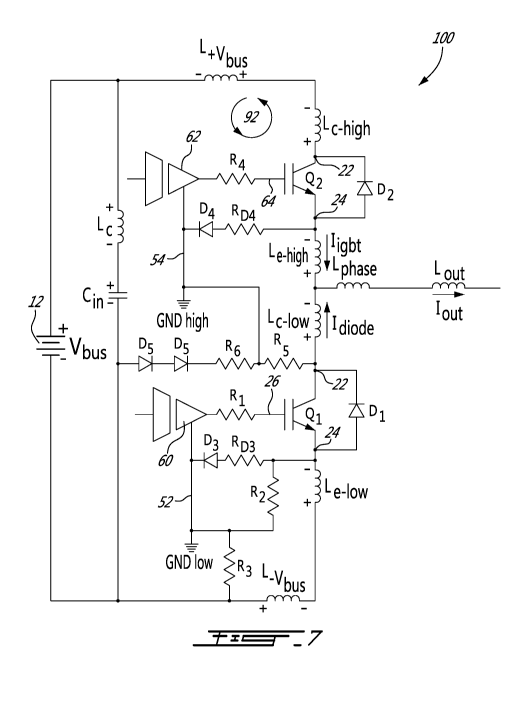
[0065] Referring now to the drawings, Figure 7 is a circuit diagram of
an
IGBT leg having turn-off diodes mounted in tandem according to an illustrative
embodiment. Several elements of an IGBT leg 100 were introduced in the
foregoing description of Figures 4 and 5 and are not described in details
hereinbelow. Generally stated, the same power electronic switches (IGBTs Qi
and Q2) and freewheel diodes (Di and D2) are placed on the same or similar
circuit card, creating the same or equivalent parasitic inductances. The
bottom
commutation cell, including the bottom IGBT Qi, the bottom gate driver 60 with
its
reference 52, and the bottom compensation circuit having the resistors R2, R3
and
RD3, as well as the turn-on diode D3, is reproduced without significant
changes.
The bottom commutation cell of the IGBT leg 100 operates in the same manner
as the bottom commutation cell of the IGBT leg 90 if the RD3 has zero
resistance
CA 02997524 2018-03-02
WO 2017/045071
PCT/CA2016/051079
17
(being a short-circuit), or in the same manner as the bottom commutation cell
of
the IGBT leg 95 if a value of RD3 is greater than zero.
[0066] The IGBT leg 100 mainly differs from the above-described circuits
by its top compensation circuit that allows the top gate driver 62 to control
the top
IGBT Q2 based on a sample of a voltage induced across the large bottom
parasitic inductance Le_k,, and across the parasitic inductance L_vbõ.
[0067] The IGBT leg 100 forms a power converter configured for limiting
switching overvoltage. Top and bottom commutation cells form a loop, being
connected at a junction of a collector 22 of a bottom power electronic switch,
illustrated as the bottom IGBT Qi, and of an emitter 24 of a top power
electronic
switch, illustrated as the top IGBT Q2. The bottom commutation cell includes
the
bottom IGBT Qi, and a bottom compensation circuit connected to a bottom
parasitic inductance that includes the parasitic emitter inductance Le_k,, of
the
bottom IGBT Qi and the parasitic negative voltage tab inductance L_vbõ. The
bottom compensation circuit applies a sample of a voltage induced across the
bottom parasitic inductance at turn-off of the bottom IGBT Qi. The top
commutation cell includes the top IGBT Q2, and a top compensation circuit that
is
also connected to the bottom parasitic inductance. The top compensation
circuit
applies a sample of a voltage induced across the bottom parasitic emitter upon
turn-off of the top IGBT Q2, when the opposite freewheel diode Di is
conducting.
[0068] Applying the sample of the voltage induced across the bottom
parasitic inductance to the bottom gate driver 60 at turn-off of the bottom
IGBT Qi
controls the voltage induced across the bottom parasitic inductance. This in
turn
limits the overvoltage on the bottom IGBT Qi. Likewise, applying the sample of
the voltage induced across the bottom parasitic inductance to the top gate
driver
62 at turn-off of the top IGBT Q2 controls voltages induced throughout the
parasitic inductance included in the loop of the IGBT leg 100. This in turn
limits
CA 02997524 2018-03-02
WO 2017/045071
PCT/CA2016/051079
18
the overvoltage on the top IGBT Q2.
[0069] Without limiting the present disclosure, the sample of the
voltage
induced across the bottom parasitic inductance upon turn-off of the bottom
IGBT
Qi is applied by the bottom compensation circuit to a reference 52 of a bottom
gate driver 60 connected to a gate 26 of the bottom IGBT Q1. Also without
limitation, the sample of the voltage induced across the bottom parasitic
inductance upon turn-off of the top IGBT Q2 is applied by the top compensation
circuit to a reference 54 of a top gate driver 62 connected to a gate 64 of
the top
IGBT Q2.
[0070] The bottom compensation circuit comprises a bottom resistive
gain adapter that includes resistors R2, R3 and RD3, as well as a turn-on
diode D3
that places a resistor RD3 in parallel with R2 when turning-on the bottom IGBT
Qi.
Values of the resistors R2, R3 and RD3 may be similar to those of the circuits
of
Figures 4 and 6, or may be selected according to the needs of a particular
application. The bottom compensation circuit applies the sample of the voltage
induced across the bottom parasitic inductance of the high frequency loop 92
at
turn-off of the bottom IGBT Qi, for example on the reference 52 of the bottom
gate driver 60, using a voltage gain Gi defined according to equation (1):
R2
= (1 )
(R2 +R3)
[0071] The bottom compensation circuit applies a sample of another
voltage induced across the bottom parasitic inductance at turn-on of the
bottom
IGBT Qi, for example on the reference 52 of the bottom gate driver 60, using a
voltage gain G2 defined according to equation (2):
(:2:RD3)
_ 2 D3 (2)
L12 r(R2.RD3)+R3)
R2+RD3
CA 02997524 2018-03-02
WO 2017/045071
PCT/CA2016/051079
19
[0072] It will be noted that given that the parallel combination of R2
with
RD3 is smaller than R2 when RD3 is not infinite, the voltage gain applied at
turn-on
of the bottom IGBT Qi is smaller than the voltage gain applied at its turn-
off.
[0073] As shown on Figure 7, the resistor R3 connects the reference 52
of the gate driver 60 downstream of the negative voltage tab. Connecting the
resistor R3 upstream of the negative voltage tab would exclude the parasitic
negative voltage tab inductance L_vbõ. It is however generally desirable to
connect the resistor R3 downstream of the negative voltage tab in order to
maximize the voltage to be sampled.
[0074] Turning now to the top commutation cell, its top compensation
circuit includes a turn-off diode D5 that connects the top compensation
circuit to
the bottom parasitic inductance upon di/dt at turn-off of the top IGBT Q2. In
a
variant, the turn-off diode D5 is selected such that a voltage drop across the
turn-
off diode D5 is greater than a voltage drop across the bottom freewheel diode
D1
when D1 is also conducting to ensure the load current will not circulate in
the
diode D5, which is a low power diode. For example, the turn-off diode may
include
a pair of turn-off diodes D5 connected in series to provide the desired
voltage
drop. Regardless of the specific configuration of the turn-off diode(s) D5,
upon
turn-off of the top IGBT Q2, a large overvoltage induced between its collector
22
and its emitter 24 causes its emitter voltage to be more negative than a
voltage of
the negative voltage tab -Vbõ. D5 therefore becomes conductive upon turn-off
of
the top IGBT Q2. In contrast, upon turn-on of the top IGBT Q2, its emitter
voltage
is higher than the voltage of the negative voltage tab
-Vbõ and the turn-off diode D5 is blocked.
[0075] It is to be noted that while the anode of diode D5 is shown
connected to the capacitor C,,, it could also be connected to GND low.
CA 02997524 2018-03-02
WO 2017/045071
PCT/CA2016/051079
[0076] The top compensation circuit comprises two resistive gain
adapters formed of resistors R5, R6 and RD4, complemented with a turn-on diode
D4. Values of the resistors R5, R6 and RD4 may differ from to those of the
circuits
of Figures 4 and 6.
[0077] Upon negative di/dt in the high frequency loop 92 at turn-off of
the
top IGBT Q2, when the turn-off diode D5 is conductive and when the turn-on
diode
D4 is blocked, the top compensation circuit applies the sample of the voltage
induced across the bottom parasitic inductance, for example on the reference
54
of the top gate driver 62, using a voltage gain G3 defined according to
equation
(3):
G3= R5 (3)
(R5+R6)
[0078] Upon turn-on of the top IGBT Q2, when the turn-off diode D5 is
blocked and the turn-on diode D4 is conductive. In that condition the top
compensation circuit applies a sample of a voltage induced across a top
parasitic
inductance that includes the parasitic emitter inductance of the top power
electronic switch Le_h,gh and optionally includes the parasitic collector
inductance
Lc-low of the bottom IGBT Qi. This sample is for example applied on the
reference
54 of the top gate driver 62, using a voltage gain G4 defined according to
equation
(4):
G. = RD4 (4)
4 (RD4 +R5)
[0079] If the value of RD4 is zero (this resistor being replaced by a
short
circuit), the turn-on of top IGBT Q2 is not impacted by the top compensation
circuit.
[0080] As shown on Figure 7, the turn-off diode D5 and the resistor R6
connect the reference 54 of the gate driver 62 downstream of the negative
voltage
CA 02997524 2018-03-02
WO 2017/045071
PCT/CA2016/051079
21
tab. Likewise, the resistor R5 connects the reference 54 of the gate driver 62
directly on the collector 22 of the bottom IGBT Qi. Connecting the resistor R5
to
the phase tab of the IGBT leg 100 would exclude the parasitic collector
inductance Lc-10w of the bottom IGBT Qi. In line with above described
reasoning, it
is generally interesting to connect the resistor R5 directly on the collector
22 of the
bottom IGBT Qi in order to maximize the voltage to be sampled.
[0081] A three-phase alternative current (AC) power source operable to
drive a motor (not shown) or a similar load can be built by combining three
(3)
IGBT legs such as the IGBT leg 100.
[0082] The foregoing describes solutions applicable to DC-DC power
converters, AC-DC power converters and to DC-AC power converters, for
example commutation cells using a full leg of semiconductors, opposite pairs
of
power electronic switches and freewheel diodes, to provide alternative current
to a
connected load such as a motor of an electric vehicle. The energy may flow
through the IGBT leg 100 in both directions, from the voltage source to the
current
source or from the current source to the voltage source
[0083] Those of ordinary skill in the art will realize that the
description of
the power converter configured for limiting switching overvoltage are
illustrative
only and are not intended to be in any way limiting. Other embodiments will
readily suggest themselves to such persons with ordinary skill in the art
having the
benefit of the present disclosure. Furthermore, the power converter configured
for
limiting switching overvoltage may be customized to offer valuable solutions
to
existing needs and problems of overvoltage occurring upon switching in power
converters.
[0084] In the interest of clarity, not all of the routine features of
the
implementations of the power converter configured for limiting switching
CA 02997524 2018-03-02
WO 2017/045071
PCT/CA2016/051079
22
overvoltage are shown and described. It will, of course, be appreciated that
in the
development of any such actual implementation of the power converter
configured
for limiting switching overvoltage, numerous implementation-specific decisions
may need to be made in order to achieve the developer's specific goals, such
as
compliance with application-, system-, and business-related constraints, and
that
these specific goals will vary from one implementation to another and from one
developer to another. Moreover, it will be appreciated that a development
effort
might be complex and time-consuming, but would nevertheless be a routine
undertaking of engineering for those of ordinary skill in the field of power
electronics having the benefit of the present disclosure.
[0085] It is to be understood that the power converter configured for
limiting switching overvoltage is not limited in its application to the
details of
construction and parts illustrated in the accompanying drawings and described
hereinabove. The proposed power converter configured for limiting switching
overvoltage is capable of other embodiments and of being practiced in various
ways. It is also to be understood that the phraseology or terminology used
herein
is for the purpose of description and not limitation.
[0086] The present disclosure has been described in the foregoing
specification by means of non-restrictive illustrative embodiments provided as
examples. These illustrative embodiments may be modified at will. The scope of
the claims should not be limited by the embodiments set forth in the examples,
but
should be given the broadest interpretation consistent with the description as
a
whole.