Note: Descriptions are shown in the official language in which they were submitted.
FLAT WEDGE-SHAPED LENS AND IMAGE PROCESSING METHOD
FIELD OF THE INVENTION
The disclosed invention generally relates to a flat lens system and correcting
aberrations of images from the flat lens system using configuration and image
processing techniques.
BACKGROUND
Anamorphic prism systems are known to compress or expand light beams, but they
have not been used for image capture for a variety of reasons. These prism
systems
are afocal, and do not focus an image onto an image plane, making them
unsuitable as
an imaging system. Typically, anamorphic prism systems are designed for
collimated
light from one incident angle and therefore their performance degrades with
off axis
light, resulting in a lens with a very limited field of view. Many anamorphic
prisms have
chromatic dispersion resulting in chromatic aberrations making them unsuitable
for
multi-color images. Accordingly, anamorphic prism systems are almost
exclusively
used to shape laser beams, often monochromatic, and are generally referred to
as
beam expanders and beam compressors.
Achromatic anamorphic prism systems, generally require multiple prisms making
them
large and heavy. In addition, since the achromatic anamorphic prism systems
only
compress or expand in one dimension, it would require multiple of these
systems to
compress equally in two dimensions to maintain the image aspect ratio, which
makes
the systems even larger and heavier. For these reasons anamorphic prism
systems
have not been used for image capture.
Imaging devices such as cameras, microscopes and telescopes can be heavy and
large. A large portion of this weight is due to the design of the optical lens
elements,
which can include heavy curved lenses, and the structure to support these lens
separated by long focal distances. These imaging devices can be large (thick)
mainly
because in a typical lens system, the opening aperture to system device depth
ratio is
-1-
CA 3021943 2018-10-24
small. Moreover, to optically improve image resolution with the traditional
lens
systems, more device depth (longer focal length) is required in order to
reduce lens
refraction and minimize lens aberrations. The device depth of the imaging
device can
limit the imaging systems' performance and design. For example, the size and
weight
constraints of mobile, compact, or weight constrained imaging devices can
limit
resolution because they constrain the maximum focal length. The disclosed
invention
can increase the effective focal length in these systems, and improve
resolution with
the same size and weight constraints.
Additionally, conventional curved lenses have many different types of
aberrations that
reduce image resolution (spherical, coma, chromatic, and others). To correct
these
aberrations, conventional curved lenses use extra large pieces of precision
glass,
adding weight, size and cost to the lens system. The disclosed invention can
reduce
the size, weight and resulting cost of conventional curved lenses, and in some
devices
eliminate their use entirely.
SUMMARY OF THE INVENTION
In some embodiments, the disclosed invention is a flat lens system which
includes: a
wedge-shaped refractive material having a first surface and a second surface
opposite
to the first surface for refracting incident light beams from an object having
a width of Y,
from the first surface towards the second surface; a reflective material
positioned at the
second surface of the wedge-shaped refractive material for reflecting the
refracted light
beams at a first angle toward the first surface, wherein the reflected light
beams are
refracted from the first surface at a second angle to compress or expand the
light from
the object having a width of X and including chromatic aberrations; and an
apparatus
for forming and processing the image of the object to reduce said chromatic
aberrations.
In some embodiments, X is smaller than Y to compress the image of the object
for use
in a telescope, for instance. In some embodiments, X is larger than Y to
expand the
image of the object for use in a microscope, for example.
-2-
CA 3021943 2018-10-24
In some embodiments, the reflective material may include one or more moving or
rotating mirrors to reflect the refracted light beams at varying angles toward
the first
surface.
BRIEF DESCRIPTION OF THE DRAWINGS
A more complete appreciation of the disclosed invention, and many of the
attendant
features and aspects thereof, will become more readily apparent as the
disclosed
invention becomes better understood by reference to the following detailed
description
when considered in conjunction with the accompanying drawings in which like
reference symbols indicate like components.
FIG. 1 shows a comparison of a tradition circular curved lens with a flat
(wedge) lens,
- according to some embodiments of the disclosed invention.
FIG. 2 shows an exemplary configuration of a flat lens system, according to
some
embodiments of the disclosed invention.
FIG. 2A illustrates a wedge-shaped refractive material, according to some
embodiments of the disclosed invention.
FIG. 3 is an exemplary process flow, according to some embodiments of the
disclosed
invention.
FIG. 4 depicts an exemplary flat (wedge) lens with a moving reflective
surface, such as
one or more moving mirrors, according to some embodiments of the disclosed
invention.
FIG. 5 shows an exemplary flat lens for expanding EM waves, according to some
embodiments of the disclosed invention.
DETAILED DESCRIPTION
Embodiments of the disclosed invention are directed to a flat lens system to
obtain a
high quality image with a more compact optical lens system and correcting
aberrations
of images from the flat lens system using configuration and image processing
techniques. Increasing the initial surface area of the lens objective
(aperture) allows
-3-
CA 3021943 2018-10-24
more electromagnetic (EM) wave energy to be collected, and can result in a
faster and
better image quality. However, increasing the aperture to improve image
quality and
speed typically results in a proportionally larger size lens system and device
depth.
The flat lens system according to the disclosed invention has an increased
initial
surface area of the lens objective (aperture), with a decreased corresponding
device
depth in the lens stack. The flat lens system collects the EM waves, such as
visible
and nonvisible lights, with a much larger aperture-to-device depth ratio. This
means
higher quality images can be captured faster with a smaller device depth. A
flat lens
system may be very large for telescopes for example, and small for
microscopes, and
yet maintain a large aperture-to-device depth ratio.
FIG. 1 shows a comparison of a tradition circular curved lens with a flat
(wedge) lens,
according to some embodiments of the disclosed invention. The figure shows how
a
flat lens system with a square light sensor can collect twice as much light as
a
conventional lens system with circular lens, and a square light sensor. As
shown, the
area 106 of the rectangular light sensor is 2r2, while the area 104 of the
circular lens is
Trr2, which is larger. The area 102 is 2r by 2r = 4r2. As seen, a flat (wedge)
lens
system captures twice the light in a device with a similar frontal area, and
therefore can
take higher quality images and do so in a faster manner. This ratio would be
even
larger for rectangular sensors, which most sensors are.
In some embodiments, the disclosed invention provides a flat lens system and
image
processing methods with an increased lens aperture to device depth ratio and
corrects
aberrations and distortions in the images produced by the lens. In some
embodiments,
the disclosed invention is capable of optical EM wave compression and/or
expansion.
Some applications for the flat (wedge) lens of the disclosed invention include
both
imaging and non-imaging applications. Examples of imaging applications are
cameras,
microscopes, telescopes, binoculars, scopes, telecentric lenses, and the like.
Examples of non-imaging applications are architectural light pipes, which
could provide
indoor illumination using natural light, and solar concentrators for more
efficient solar
energy generation.
-4-
CA 3021943 2018-10-24
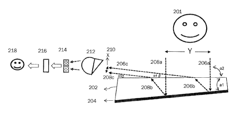
FIG. 2 shows an exemplary configuration of a flat lens system, according to
some
embodiments of the disclosed invention. A wedge shaped refractive material 202
with
angles al and a2 is formed on top of a reflective surface 204 to form a flat
lens. The
image of an object 201 with a width of Y is reflected from multiple surfaces
of the flat
(wedge) lens, processed and compressed to form a compressed image 218 of the
same object. As shown, light (EM) waves 206a and 208a at the two ends of
object 201
are penetrated into the refractive material 202 and reflected from the
reflective surface
204 at an angle to form light waves 206b and 208b, respectively. The reflected
lights
(EM) 206b and 208b are further reflected from the internal surface of the
refractive
material 202 to form light waves 206c and 208c, respectively. The angle of the
light
waves 206c (a4) and 208c (a3) leaving the refractive material can be designed
for
specific applications, using conventional optical design methods. Reflected
light waves
206c and 208c now form a smaller size X (compressed) image 210 of the original
object 201.
Varying angles al and/or a2 will vary the size X of the compressed image 210.
The
size X of compressed image 210 varies with the EM wavelength, angle al and a2,
and
the type of the refractive material 202. Angles al and/or a2 values can be
varied for
specific applications, such as the degree of the compression (X) needed. In
many
typical applications, angles al is between 15 and 25 degrees and a2 is between
75 to
105 degrees. Exit beam angles of a3 and a4 can be modified by varying angles
al
and/or a2 until the critical angle is reached which then alters the beam path
to total
internal reflection.
Referring back to FIG 2, the compressed image is then directed to an optional
focusing
lens 212 to focus the compressed image onto light sensor(s) 214 (for example,
CCD or
CMOS sensor(s)). In some embodiments, the focusing lens 212 focuses the
compressed image onto an eyepiece for viewing by a human. An image processor
216
(implemented in software, hardware and/or firmware) corrects for any
aberrations
resulting from the lens system by using one or more image processing
techniques. An
example of correcting chromatic aberrations in hardware would be the use of
one or
-5-
CA 3021943 2018-10-24
more optical wedges and/or diffraction gratings, before the light sensor 214,
that
together have an achromatic effect for imaging. The refractive properties of
the
material of the wedge 202 can be changed to assist in controlling chromatic
dispersion
for imaging applications as well. For example, the refractive index of the
wedge can be
dynamically changed by applying voltage to current to the wedge comprised of
certain
material that refract the light differently under electric power.
If the image processing is performed by an optical device (hardware), the
correction is
done before the image is received by the sensor. However, if the image
processing is
performed by software (executed on a processor), the corrections are performed
after
the image is received by the image sensor, that is, at the output of the
sensor.
In some embodiments, the chromatic dispersion for the output image is
dynamically
measured (for example, at predetermined intervals) and a corresponding voltage
(or
current) is applied to the wedge to change its refractive index and/or its
beam
absorption to compensate for the measured chromatic dispersion. In
some
embodiments, the amount of the voltage (or current) applied to the wedge is
determined from a stored lookup table, taking into account the measured
chromatic
dispersion and the type of the wedge material.
Characterizing the chromatic dispersion per device, and applying software
algorithms
in the image processor 216 to the image, can also be used to assist in
controlling
chromatic dispersion for imaging
There are many known image processing techniques to correct for image
aberrations.
One method is to calculate or measure the aberrations of the system, for
example, by
creating spot diagrams, which are different for each wavelength of light, and
then apply
an inverse transfer function to reverse these aberrations.
The refractive material 202 may be made of any type of glass, plastic, fluids
such as
water, or similar types of refractive materials. In case of a fluid, such as
water, the fluid
may also be used to allow cooling of the optics. The reflective surface 204
may be any
type of mirror or other material having a reflective surface. Such reflective
surface may
be attached or coated on such material to form the reflective surface 204.
-6-
CA 3021943 2018-10-24
The flat lens of the disclosed invention may have any rectangular shape,
rather than a
square shape, which allows for variable compression ratio and aspect ratio of
the
image being formed. In some embodiments, the wedge angles al and a2 can be
variable as the specific applications require. For example, using common BK7
glass, a
typical wedge angle a2 may vary between 75 and 105 degrees, in some
embodiments.
Choosing an angle a2 closer to 75 degrees will result in higher energy
captured and
lower chromatic aberration but have lower compression. However, choosing an
angle
a2 closer to 105 degrees results in a higher compression of the image at the
expense
of higher energy losses and larger chromatic aberration. Angle al can be
varied to
produce similar effects.
Although FIG. 2 and its description is directed to visible light and an image,
those
skilled in the art would recognize that the flat lens of the disclosed
invention is not
limited to visible light. Rather, the disclosed invention is capable of
operating on any
type of EM wave that can refract, with or without forming an image. Moreover,
any
combination of the optional components 212, 214, and 126 with the refractive
material
202 and reflective surface 204 is possible and within the scope of the
disclosed
invention.
FIG. 2A illustrates a wedge-shaped refractive material (prism), according to
some
embodiments of the disclosed invention. As shown a reflective material is
coated or
attached to the back of the wedge-shaped refractive material. The wedge-shaped
prism has a vertex angle a (e.g., between 2 and 25 deg.). If one surface of
the prism is
reflectorized (by the reflective material), a thin anamorphic beam expander
/compressor can be created. In this case, it is shown that the output beam is
orthogonal to the input beam. Although FIG. 2A, illustrates a reflecting wedge
anamorphic compressor prism that converts an input beam with an aspect ratio
of, for
example, 2:1 to an output beam with an aspect ratio of, for example, 4:3, one
skilled in
the art would recognize that any prism designed for anamorphic compression can
be
used as an expander by reversing the direction of the input and vice versa.
The ray-
trace equations of the prism are
-7-
CA 3021943 2018-10-24
(1)
(sin /,
= arcsin (2)
n
12 = a + = /21, (3)
= + - - 4), (4)
/3' = arcsin(n sin /3), (5)
(6)
Here, a 2-= (/3 - /1' )/2 and 4) is the tilt angle of surface 1 from the
vertical. 4) and a may
be adjusted until the desired compression or expansion ratio is obtained. For
instance,
for a prism of B270 optical crown glass (nd = 1.5229) with 4) = 16.9 deg and a
= 14.0
deg, an anamorphic compression A'/A = MAG 0.375 can be obtained. Typically,
two
of these reflective wedges, placed orthogonally to maintain the image aspect
ratio,
would result in a shortening the focal length required of the focusing lens
system by
50% or more. This effect may be used to create a more compact device.
Compressing the image using this technique allows the image to be focused in a
shorter distance while maintaining resolution. A shorter focal distance allows
for a
more compact device. This means higher quality images can be captured faster
with a
smaller lens system. FIG. 3 is an exemplary process flow, according to some
embodiments of the disclosed invention. In block 302, an EM energy (which may
or
may not contain an image) enters an optical system comprising one or more flat
(wedge) lens. The EM energy goes through the medium and bounces off a
reflective
surface, in block 304. In this example, it is assumed that the EM wave is
visible light
forming an image. However, as explained above, the disclosed invention is not
limited
to visible light and images, rather, it is applicable to any EM wave/energy.
The
reflected EM wave then travels through the medium and exits the optical
elements, in
block 306, where the EM wave will be compressed or expanded in one or more
plane(s). In block 308, the EM wave may then travel through an optional
modifying
(focusing and correcting) lens system. In block 310, the EM wave strikes one
or more
EM sensor(s) or optical element(s) for human eye viewing. Block 302 to block
308
-8-
CA 3021943 2018-10-24
may be repeated multiple times to compress the EM Wave in multiple planes. In
the
case of imaging, the compressed output aperture from 306 reduces the required
focal
length which reduces the corresponding device size. In block 312, a processor,
such
as an image or EM wave processor, receives the information from the EM sensor
and
modifies/enhances this information, as required by the application of the flat
lens. This
can also be used to expand/spread the image if the application is directed to
a
microscopic function, where the sequence is partially reversed.
In block 314, in the case of imagery application, the (image) processor
corrects
aberrations from the lens system. The refracting wedge lens can introduce
chromatic
aberrations, but does not introduce other aberrations usually associated with
circular
lens systems. The chromatic aberration can be predetermined (by calculation or
measurement) for each pixel. A table can be used to offset each color at each
pixel to
reposition the pixel at the appropriate position in the resolved image.
Alternatively, or in combination, hardware (optical) processing of the image
may be
performed by achromatic elements, such as achromatic wedge(s). The anamorphic
prism is formed as an achromatic structure using a first prism and a second
prism. The
refractive indexes and refractive index changes as a result of a wavelength
fluctuation
of the first and second prisms and an incident angle of the beam to the first
prism can
satisfy a predetermined relationship, where the beam can emerge from the
second
prism at an exit angle of 0 degree, which corrects the anisotropy of the angle
of the
beam.
The flat lens system of the disclosed invention collects the EM waves, such as
visible
and/or non-visible light, with a much larger aperture-to-device depth ratio.
This means
higher quality images can be captured faster with a smaller lens system.
The flat lens system may be very large for telescopes for example, and small
for
microscopes, and yet maintain a large aperture-to-device depth ratio. The
image
sensors are often charge coupled devices (CCDs) or CMOS sensors. The disclosed
invention is not limited to the above examples of imaging sensor, rather,
other types of
EM or imaging sensors may be used with the flat lens of the disclosed
invention.
-9-
CA 3021943 2018-10-24
Human eye viewable optical elements may also be used. In the case of human eye
viewable optical elements, blocks 308 to 314 may not be required because the
human
eye can focus the image.
In block 312, one or more processor(s), such as an image or EM wave
processor(s),
receives the information from the EM sensor(s) and modifies/enhances this
information, as required by the application. This can also be used to
expand/spread
the image if the application is directed to a microscopic function, where the
sequence is
partially reversed.
In the case of a three dimensional (3D) imaging, more EM sensors may be
required, as
known in the art. The invention is not limited to the above examples of
imaging sensor,
rather, other types of EM or imaging sensors may be used with the flat lens of
the
disclosed invention.
FIG. 4 depicts an exemplary flat (wedge) lens with a moving reflective
surface, such as
one or more moving mirrors, according to some embodiments of the disclosed
invention. As shown, the image of an object 401 is reflected from multiple
surfaces of
the flat (wedge) lens, processed and compressed to form a compressed image 414
of
the same object. Light (EM) waves at the two ends of object 401 are penetrated
into
the refractive material 402 and reflected from moving mirrors 404 at varying
angles to
form a smaller size (compressed) image 406 of the original object 401.
The compressed image 406 may optionally get directed to an optional focusing
lens
408 to focus the compressed image onto light sensor(s) 410 (for example, CCD
or
CMOS sensor(s)). An image processor 412 (implemented in software, hardware
and/or firmware) corrects for any aberrations resulting from the lens system
by using
one or more image processing techniques and output a corrected compressed
image
414. If the image processing is performed by an optical device (hardware), the
correction is done before the image is received by the sensor. However, if the
image
processing is performed by software (executed on a processor), the corrections
are
performed after the image is received by the image sensor, that is, at the
output of the
sensor. Moreover, any combination of the optional components 408, 410, and 412
-10-
CA 3021943 2018-10-24
with the refractive material 402 and the optional components 212, 214, and 126
(depicted in FIG. 2) is possible and within the scope of the disclosed
invention.
In these lens systems with moving reflective surface, the quality of the image
is
increased by reducing the field of view, and stitching many images together.
This
technique can improve final image resolution. Moving the mirror changes the
view of
what objects appear in the image. In these embodiments, the mirror is mOved in
a way
that it can captures a series of images, each with a narrow field of view. The
system
then uses known image processing techniques to combine or stich the captured
images together into one composite image with a large field of view. For
example,
known image stitching methods may be used to register, calibrate and blend the
images to produce the final image 414. Because the imaging system has a
relatively
large aperture size with lots of light, images can be captured very quickly.
Another
reason to move the mirror is to adjust the field of view, or change the
compression of
one single image, for example, for digital or optical zooming applications.
There are several different techniques to move the mirror 404. Although mirror
404 is
shown as rotating, in some embodiments, it is possible to tilt the reflective
surface
(e.g., a mirror) about a fulcrum, or rotate about the edge as shown in FIG. 5.
In some
embodiments, the mirror can be an array of micromirrors. The moving reflective
surface(s) of the flat lens system may be combined with the dynamic changing
of the
refractive index of the refractive wedge-shaped material (as described above)
to further
enhance the lens system.
FIG. 5 shows an exemplary flat lens for expanding EM waves, according to some
embodiments of the disclosed invention. FIG. 5 described below, illustrates a
microscopic function, where the EM paths are reversed with respect to those
depicted
in the example of FIG. 2. Light leaves a small size (X) object 502, and enters
a wedge
504 where it is expanded, and reflected off a reflective surface 506, such as
a mirror.
The light then exits the wedge into a lens system 510, light sensor 512, and
image
processor 514. The processed image is an expanded image 516 of the small size
image 502. Further expanding the expanded image 516, for example, by varying
the
-11-
CA 3021943 2018-10-24
angle al and/or a2 and/or a3 and/or configuring multiple wedges in series to
further
expand the small object image 502, the function of a microscope can be
realized with a
much smaller device and/or enable higher resolution and/or viewable area. In
some
embodiments, the wedge may include an anti-reflective coating(s) to capture
more of
the light energy leaving the small object. Similar to flat lens systems of
FIG. 4, if the
image processing is performed by an optical device (hardware), the correction
is done
before the image is received by the sensor(s). However, if the image
processing is
performed by software (executed on a processor), the corrections are performed
after
the image is received by the image sensor(s), that is, at the output of the
sensor(s).
There are several known image processing methods to correct the image
aberration
caused by the flat lens. The use of these known methods is dependent upon the
application of the flat lens. For example, lookup tables may be used to
correct the
aberrations as a relatively simple correction for chromatic aberrations.
Moreover,
transfer functions may be appropriated when fixing chromatic aberrations in a
flat lens
.. application.
In some applications, there may be a low intensity of EM energy, such as in
low light
applications (e.g., night vision, or for example Raman Spectroscopy of
biological tissue
where high power lasers may damage the tissues). In these applications, the
large
aperture of the lens system of the disclosed invention is capable of
collecting a large
amount of light energy, and still use a very compact design.
In some embodiments, the disclosed invention is capable of capturing and
optionally
process multispectral or hyperspectral imaging, which is used to collect and
process
information from across the electromagnetic spectrum to obtain the spectrum
for each
pixel in an image of a scene, with the purpose of finding objects, identifying
materials,
or detecting processes in the image of the scene.
In some embodiments, the disclosed invention is scalable and applies to a full
range of
system sizes including those from small microscopic/nano systems to large
telescopic
systems greater than, for example, 30m is length or diameter.
-12-
CA 3021943 2018-10-24
It will be recognized by those skilled in the art that various modifications
may be made
to the illustrated and other embodiments of the invention described above,
without
departing from the broad inventive scope thereof. It will be understood
therefore that
the invention is not limited to the particular embodiments or arrangements
disclosed,
but is rather intended to cover any changes, adaptations or modifications
which are
within the scope of the invention as defined by the appended claims and
drawings.
-13-
CA 3021943 2018-10-24