Note : Les descriptions sont présentées dans la langue officielle dans laquelle elles ont été soumises.
CA 02601001 2013-08-26
EI-Zcrr,g0.$TATTICATX).',RECiPLATED ATC1,1!$,K
$:Ats iRõapT.T3,0c9NpucTlyt.r. Ypgywi:E:
gEt.A.7p APpg:c4v.rioN::
=
FLELD OJ !TilitE INVENT:01C-
The:.:present iverition. :relates: ix) the placement :of an, atom Or
'Iuniecale
:proNtimily to an eleatmotatic: potential extending.:frem
:K.:charge:di:single.. atom and ni
10. iuIai: tocontraled :manipulation :of: the electitatw. potential to.
f,-,;inate.
linoleduiatAranaistor;
PACKGRO.T.IND'OF
rgdgmfM ja.r,eti the: 01,ity
of $ingle tboiemila 6.1ottical
.44.110014, !go0Or.4.4.
pqii6.(1:144.y of: = :t.%.*41=:.:er.tilih.ift .8thittottg are ineteasingly
15: :17.0,0t.:0114.t*prtx10i4blia:.c.k.4_,.. :Moleentat
pi;iVe-ttid are highly dellendent or'
;Ed6t4iiii:ot tru Mt and. tonipoittkin; Recent liieetetiCal and txpetittehtal
weik ba
'shown. illat...tranapott: pioperries too can chsng:. encirknotiSly:',aS 4
tittplit.=otatoin4061
sun:Ulna = vatiatiOna (7, 8, 9 10 1.1, 12),It it. 'Cleat: that the.'; fUl-
petentiat ef
Inolectflat: devices:will be: :unvelled..only when :meticulous attic:0ga1
imowledge. and
26, :cnntrd is in hand..
It la_ equally vtai, 1.11:tmvegie=.f.:Qr. an .;(eleciroStatic cent:pot of
:eormot
-titro4giaa 4ce): dated deliieca ¨ well as yaztnim, tube
,trapai$0.m. re ik rabk hix aue dry 4,49.,. ,At
4yuo*.l.vcorifigpi,=:40011.
.flosw, in cirewts 0*: F.61*m to tu4viig
ga#,d.n.OlecuW con4uctiOniS:
that there:Simply i inetifficiont to luty.c:';
000 axt.p.pd4 yoluiptt
th ,*p:!.,of,.:.fe..r:(!ikarilP).0 alitinT:ene-:inOiledale 0.4 A omprimI n
be0.16do
oo.otkoe$:,p thc:i)rOt76,ile whie thltd beeeAsarily in re
:41attint eled4'000 u a g bt poor gate eftic y rt.u1l
14); A.:
:railical1y.diffel!ent.appteatili'appea0V he 'tell-ate&
CA 02601001 2007-09-10
WO 2006/095252
PCT/1B2006/000510
2
Current three-terminal single molecule device schemes have focused on
phenomena such as Kondo resonance or single electron (Coulomb blockade)
physics
that require cryogenic conditions to operate (15, 16). An alternate scheme,
capable
of room temperature switching behavior, is a prerequisite (but not sufficient)
quality
for molecular electronics to advance.
While active molecular technologies face many additional challenges, the
need for detailed structural control, for strategies to achieve gated
molecular
conduction, and for room temperature operation are the most substantial
obstacles to
be overcome.
One way to satisfy these requirements is to study molecules bound to order
surfaces, such as silicon, with using scanning tunneling with quantum
mechanical
(17) and classical electrostatic simulations and analysis. In this way, atomic
structure and electrostatic potential variations that affect the properties of
an
individual molecule are understood. In spite of efforts to understand and
ultimately
control electroconductivity on an atomic scale, systematic and controlled
building of
devices on this scale has proven difficult.
Thus, there exists a need for an electrostatically regulated atomic scale
electroconductivity device, such as a molecular transistor. Additionally,
there exists
a need for a process to build such a device that is amenable to manufacturing
and a
variety of operating environments.
BRIEF DESCRIPTION OF TEE DRAWINGS
Fig. 1(A) shows the slope effect across a molecular line ¨ visualizing
electrostatic potential emanating from a point source. STM image of highly n-
type
doped H-Si(100). Negatively charged "dangling bonds" are labeled "DB1" and
"DB2", where the prominent white bar is a line of surface-bound molecules. At
elevated sample bias, -2.4 V, molecular it-states are "turned on" causing
molecules to
appear bright (topographically elevated) and of near constant height across
the line.
Fig. 1(B) shows that at an intermediate bias, -1.8 V, molecules appear darker,
increasingly so at greater distances from the dangling bond DB1. Fig. 1(C)
shows
that in the absence of a negative DB all molecules would appear dark at -1.6
V, but it
is seen that molecules nearest the DB remain prominent. Molecules near the DB
CA 02601001 2007-09-10
WO 2006/095252
PCT/1B2006/000510
3
experience a greater effective tip-sample bias due to the negatively charged
DB's
electrostatic potential. The inset is a Si(100) schematic. Fig. 1(D) is a
cross
sectional occupied state height profile taken along the molecular line for Vs
= -2.4 V,
-2.2 V, -2.0V, -1.8 V, and -1.6 V. The effect of DB2 is particularly evident
as a
hump in the -2.0 V cross section. Fig. 1(E) is a graphical representation of
cross
sectional occupied state height along an underlying line of styrene molecules
proximal to a dangling bond. Images and line scan data were acquired at a
constant
tunnel current of 40 pA. Image areas: 10.6 nm x 10.6 nm.
Fig. 2 shows an STM image of slope-free styrene lines on low doped n-type
H-Si(100). Dangling bonds are indicated by arrows. Under these imaging
conditions (Vs = -2.0 V, 80 pA), dangling bonds are neutral, and no
significant
height perturbation is observed along the molecular lines. Image area: 18 nm x
18
nm.
Fig. 3 shows the 12 nm x 12 nm STM images acquired at -1.9 V and 50 pA.
Fig. 3(A) shows sloping styrene lines with a dangling bond at the end of each
line, as
indicated by arrows. Fig. 3(B) shows one 2,2,6,6-tetramethyl-1-piperidinyloxy
(TEMPO) molecule reacted at each dangling bond as indicated with wedges.
Charge, and therefore slope, are absent. Fig. 3(C) shows TEMPO molecules that
are
removed by scanning at -3V. The charged dangling bonds are regenerated, as
indicated by arrows, and the slope reappears. Fig. 3(D) are height occupied
state
profiles of styrene lines from the upper left corner of Figs. 3(A)-(C) shown
in green,
black and red, respectively.
Fig. 4 shows on the left side representative orbitals showing that the highest
energy molecular state is localized near the negative dangling bond (indicated
by the
purple sphere and arrow) while molecular states deeper in the occupied
manifold are
localized farther from the negative dangling bond (top to bottom); on the
right side
charge density surfaces of molecular states as a function of energy, with the
top state
being the charge density of the highest molecular state, with each subsequent
surface
representing the sums of charge densities of molecular states from the top of
the
valence band to the indicated energy. These surfaces demonstrate that the
slope
effect appears at smaller magnitude scan biases and disappears (images become
flat)
CA 02601001 2007-09-10
WO 2006/095252
PCT/1B2006/000510
4
at higher magnitude scan biases in agreement with the STM measurements. For
clarity, a row of silicon dimers has been removed from the model.
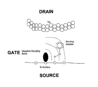
Fig. 5 shows a graphical representation of a single molecule transistor,
showing the silicon substrate (source), dangling bond (gate), tunnel electrode
(drain),
molecule and tunnel gap (channel). The electrostatic potential emanating from
the
dangling bond is indicated by curved red lines of decaying intensity.
Fig. 6(A) shows a current-voltage graph of styrene molecules at varying
distance from the negatively charged dangling bond. The black curve (acquired
closest to the DB) sees a greater effective sample-tip (source-drain) bias,
and
displays a lower onset voltage and greater overall current than curves
acquired
farther along the molecular line. Inset shows ratio of source-drain current
measured
at 4 Angstroms and 58 Angstroms from the DB.
Fig. 6(B) shows a graph of source-drain current as a function of gate voltage
(dangling bond potential) for varying source-drain voltages. A
maximum
transconductance of ¨0.26 nA/V is observed for Vsd=-2.0 V.
Fig. 7 shows a graph of the change in the calculated it x-state and it y-state
in
a single substrate-bound styrene molecule as a function of inverse distance to
the
dangling bond.
Fig. 8 shows a schematic of a representative donor-bridge-acceptor system
coupled to a charge receptor and a perturbing soluble charge entity according
to the
present invention.
Fig. 9 shows a schematic of a device for selectively controlling the
electronic
charge on a single atom.
SUMMARY OF THE INVENTION
An atomic scale electroconductivity device with electrostatic regulation
includes a perturbing species having a localized electronic charge. A sensing
species
having an electronic conductivity is placed in proximity to the perturbing
species at a
distance sufficient to induce a change in the electronic conductivity
associated with
the localized electronic charge. Electronics are provided to measure the
conductivity
via the sensing species.
CA 02601001 2007-09-10
WO 2006/095252
PCT/1B2006/000510
A temporally controlled atomic scale transistor is provided by biasing a
substrate to a substrate voltage with respect to ground. A dangling bond
extending
from a substrate atom has a charge state from among a charge state group. The
charge state varies in units of single electron addition or withdrawal. A
grounded
5 electrical contact is provided within a localized electronic charge in
proximity to the
dangling bond. A sensing species having an electronic conductivity is also
placed in
proximity to the dangling bond. A sensing species contact biased with respect
to said
substrate is provided such that varying the substrate voltage modifies the
charge state
of the substrate atom at one electron unit of charge and still within the
charge state
group for the substrate atom. The dangling bond functions as a single atom
gate
electrode. By placing the dangling bond in an array of sensing species, an
atomistic
multi-channel gate transistor is formed.
A process for operating an electrostatically regulated atomic scale
electroconductivity device includes charging a perturbing atomic or molecular
species having a localized electronic charge associated therewith so as to
induce an
electrostatic field. By monitoring electronic conductivity through a sensing
atom or
molecule in proximity to the electrostatic field, an atomic scale device is
formed.
DETAILED DESCRIPTION OF THE INVENTION
The present invention has utility as an atomic scale electroconductivity
device.
An inventive device has a single or a collection of atoms or molecules
(perturbing species) which carry localized electronic charge (in the form of a
monopole, dipole, or otherwise). A single or a collection of atoms or
molecules
(sense species) is provided in sufficient proximity to the perturbing species
(ones,
tens, hundreds, thousands of angstroms) to detect the presence of the
electrostatic
field emanating from the perturbing species, as evidenced by changes to the
electronic conductivity of the sense species, and electronics measuring
conduction
through said sense species.
The sense species can be implemented in the solid state. It may be positioned
with its associated contacts on a solid surface and placed against a liquid,
gas, or
vacuum environment, or fabricated at the interface between two solids. It may
also
CA 02601001 2007-09-10
WO 2006/095252
PCT/1B2006/000510
6
be encapsulated by a solid or liquid. Interaction with the perturbing species
then
occurs by chemical reaction, and/or contact, and/or physisorption of
perturbing
species with the outer walls of the encapsulant, and/or by reaction and/or
diffusion
into the bulk of the encapsulant. Alternatively, the sense species is a single
or
collection of ionized impurity atoms or molecules (residing on, in, or above a
surface, coupling to a donor-bridge-acceptor charge transfer complex, or
within a
bulk solid), optionally associated with a point defect, a collection of point
defects
(such as an interstitial, vacancy, substitutional impurity (including dopants)
etc.), or a
domain or intergrain boundary, or combination thereof.
When the sensing species is a dopant, the temperature dependent, variable
degree of ionization of that species allows an inventive device to serve as a
thermometer. At low temperature, a dopant is rarely ionized (usually neutral);
at
high temperature, the dopant becomes ionized (charged), thereby forming a
robust
solid state device.
It is appreciated that the sense species and/or perturbing species optionally
exists independently as a single or a collection of atoms or molecules in the
liquid
phase or in a gel, in solution or in suspension (e.g. colloidally) or in the
gas phase.
The electrical contacts are patterned on a substrate (solid or gel), with the
sense and
perturbing molecules being provided by the gel, liquid, or gas phases. A
soluble
perturbing species that diffuses through a solution to interact with a sensing
species
is susceptible to temperature-dependent diffusional rate changes associated
with
solution viscosity or ionicity.
The relative number of sensing species to perturbing species and known
states of sensing species can be used to infer information about the
perturbing
species.
A single sense species used to determine the charge state of a single
perturbing species in implementations where the spatial relationship between
the
location of the sense species and the functionalized group which localizes the
perturbing species is known. In this case, the shift in the IV characteristics
of the
sense molecule is inferential of the charge state (quantity and sign) of the
perturbing
species. A single sense species used to determine the distance between the
CA 02601001 2007-09-10
WO 2006/095252
PCT/1B2006/000510
7
perturbing species and the sense species, in implementations where the charge
state
of the perturbing species is known based on knowledge of the local chemistry
occurring in a particular application. Variation in the IV characteristics
across the
sense molecule is inferential of the distance between the perturbing species
and the
sense species. Arrays of individual sense species, with precise knowledge of
the
relative spatial coordinates between each of the sense species, are used to
determine
the position and charge state of a single or collection of perturbing species.
A single
or collection of sense species are used to map out electrostatic fields (i.e.
more
sensors = greater spatial resolution/precision).
The sense species is operative as a sensitive probe of localized, transient,
or
electrostatic perturbations itinerant, where itinerant charges may correspond
for
instance to mobile charges, ions, or discrete multipole charges distributions
within a
solid, liquid or gas medium. Large changes in conductivity across the sense
species
result from the presence of local electrostatic fields. The sensitivity of
current
transport mechanisms to the local charge environment allows the charge state
of the
perturbing species to be deteimined without modifying its charge state.
The present invention affords a reading capability for a quantum dot cellular
automata (QCA). Since a QCA paradigm uses single electrons in interaction with
quantum dots to encode and process binary information, the polarizations
associated
with a single electron interacting with a quantum dot represents a QCA logic
level.
It is appreciated that a sense species according to the present invention is
readily
employed to read the logic level of a QCA. Additionally, it is appreciated
that a
QCA analog is formed through the use of a dangling bond in place of a quantum
dot
while multiple quantum dots within a QCA type array to accord molecular
polarization logic levels analogous to those obtained by single electron
injection into
a quantum dot system.
As a transistor, an inventive device can be operated with nanoampere current
levels across the source-drain contacts. It is appreciated that a current
several orders
of magnitude lower or higher is operative, depending solely upon the
sensitivity of
the external circuit which measures the IV characteristics of the sense
species and/or
fundamental intrinsic noise limitations relating to the carrier transport
mechanism
CA 02601001 2007-09-10
WO 2006/095252
PCT/1B2006/000510
8
operating across the sense species for example, shot noise in current flowing
across
the sense species. It is appreciated that an array of inventive devices
operating as a
transistor generate a quantum computing architecture.
Sense and perturbing species join together by chemical and/or physical
interactions. Contacts to the sense species are made by zero, one or multiple
individual chemical groups each including a single or a collection of atoms or
molecules, hereafter referred to as "contact species", bound or physisorbed to
the
sense species. The collective electromagnetic absorption and/or emission
properties
of the sense and contact species are dependant upon the electrostatic and/or
dispersion induced modification by the perturbing species. The charge state
and/or
chemical identity of the perturbing species is inferred from changes induced
in the
electromagnetic absorption and/or emission spectra of the collective sense,
perturbing, and contact species.
Alternatively, the contact species operates as a trigger with the
electrostatic
and/or dispersion induced shifting of the electronic levels in the sense
species under
the influence of the perturbing species causes the trigger contact species to:
i) undergo chemical fission into identifiable (via electromagnetic
spectroscopy or
mass spectrosmetry) products released into the local environment, ii) chemical
fusion
with other chemical species present in the local environment, iii) chemical
fusion
with other chemical species in the local environment leading to a chain
reaction until
depletion of reactants occurs, or iv) a combination of chemical fusion and
fission
processes which lead to replication of one or more copies of the initial
configuration
involving a single sense species coupled to newly formed trigger contact
species.
In the event that the charge gated molecule is employed in the liquid phase,
the sense species is optionally free of electrical connections to a solid
substrate. The
sense species can serve as an electron bridge between donor and acceptor
molecules.
Bridge mediated electron transfer in donor-bridge-acceptor complexes is known.
In
those cases, the bridge is always "on". Electron transfer happens whenever the
donor
molecule is electronically excited. By choosing a bridge that is normally in
the "off'
state, but which is rendered "on" when a charged species is nearby, allows a
new
CA 02601001 2007-09-10
WO 2006/095252
PCT/1B2006/000510
9
mode of operation of a donor-bridge-acceptor complex. Normally on and charged
induced off behavior is also possible.
Changes induced in the electromagnetic absorption and/or emission spectra of
the donor-bridge-acceptor complex allow modified transport to be detected.
Such a
complex is therefore an indicator of the presence of the perturbing species.
Chemical functionalization of the bridge species allows selective interaction
with perturbing species, lending a discriminating detector function to the
complex.
The donor-bridge-acceptor complex also optionally contains a tethered charged
(or
multipolar) receptor moiety. In that case, the charger receptor acts as a gate
that is
regulated by the near approach of solution perturbing species of contrasting
dielectric
qualities. Fig. 8 shows a donor-bridge-receptor complex coupled to a charge
receptor susceptible to soluble charged species perturbation. The solution
species are
readily coupled into a network ¨ a kind of integrated circuit ¨ allowing logic
and
other functions to be performed upon chemical stimulus. Whether in liquid
phase or
when substrate mounted to a solid substrate, charge mediated conductivity of a
sensor molecule can be employed as a chemical trigger. For example, a redox
chemical transformation can be driven by the electron arriving at the acceptor
molecule.
A charge receptor amenable for coupling to a donor-bridge-acceptor complex
90 illustratively includes a heterobenzyl quaternary ammonium salt and
especially those
containing a thenyl methylene group; metal doped fluorines, and proteins such
as
rhodopsin. By way of example, 1-anilino-8-naphthylene sulfonate is known to
operate as a soluble charged entity that tightens protein confirmations (18).
The
coupling of such a protein to a donor-bridge-acceptor complex is
representative of an
operative device according to the present invention.
The perturbing species is an atom or molecule (single or collections thereof)
being members of a solid, liquid, or gas phase environment (and/or solutions
thereof). In a solid, the perturbing species is optionally a single or
collection of
ionized impurity atoms or molecules, residing on, in, or above a surface, or
within a
bulk solid. The perturbing species may also correspond to a point defect, a
collection
of point defects (such as an interstitial, vacancy, substitutional impurity,
etc.), or a
CA 02601001 2007-09-10
WO 2006/095252
PCT/1B2006/000510
domain or intergrain boundary, or any collection of these which offers the
ability to
localize charge. In a liquid, the perturbing species may be provided by ions
or
molecules with multipole charge moments.
It is appreciated that a perturbing species optionally forms a polarizable QCA
5 element
analogous to a quantum dot, with the added advantage of being readable via
a sensing species. A QCA device analog according to the present invention
affords
an advantage of a stable polarized state, in comparison to the state decay
associated
electron trapping by a quantum dot.
The perturbing species is also operative as a passive device element. Under
10 regimes
where strong coupling between the current flowing across the sense species
and the perturbing species exists, the charge state of the perturbing species
is
dependent upon the magnitude or direction of current flow through the sense
species.
This results in bi-stability or negative differential resistance, or
hysteresis in the IV
characteristics across the sense species. Such an effect is employed to yield
non-
linear device elements suitable for fabricating logic circuits or analog
signal
processing circuits.
A solid substrate operative to construct an inventive atomic scale
electroconductivity device has the attribute of defining at least one
electrical contact
to a perturbing species, and at least mask, or electron beam writing on a
sacrificial
mask. After patterning, a metal layer is deposited through vacuum deposition,
sputtering or electrodeposition. This substrate for metal ion deposition
includes a
variety of insulative surfaces. Suitable substrates illustratively include a
silicon
wafer, mica, ceramics, and silicates.
In inventive embodiments where perturbing species and sensing species fuse
in adhered proximity to the electrical contacts, an operative device is
completed by
providing a secondary electrical contact to the sense species. In those
embodiments
where the perturbing species is a solid state component, a perturbing species-
forming
material overlays a patterned contact on the substrate. Materials suitable for
the
generation of a perturbing species illustratively include semiconductor
domains
having incomplete surface passivation, specific forms of which include
protonated
surface, locally doped and nanocrystalline domains of semiconductors
illustratively
CA 02601001 2007-09-10
WO 2006/095252
PCT/1B2006/000510
11
including silicon, a variety of extrinsic and intrinsic monoatomic, binary and
ternary
semiconductors illustratively including silicon, gallium arsenide, gallium
phosphide,
indium phosphide, germanium, indium arsenide, indium antimonide, gallium
aluminum arsenide, cadmium sulfide, zinc sulfide, aluminum indium phosphide,
aluminum gallium arsenide, aluminum indium arsenide, aluminum gallium
antimonide, gallium indium phosphide, lead tin telluride, copper gallium
selenide,
zinc germanium arsenide, and copper iron sulfide. The patterned deposition of
semiconductors is well known to the art as embodied in U.S. Patents 4,180,604;
4,745,042 and 5,627,090. Localized implantation of dopants to a semiconductor
to
form perturbing species is achieved through a variety of techniques including
laser
implantation (18), electrostatic potential accelerated ion implantation (19)
and
absorption of atomic or molecular dopants from a fluid gaseous or liquid
phase.
Alternatively, a semiconductor nanocrystal is covalently bound to an
underlying
substrate or electrical contact through the use of a self-assembled monolayer.
An
exemplary procedure for nanocrystal adherence through a self-assembled
monolayer
is detailed in U.S. Patent 5,751,018. It is appreciated that a semiconductor
is
optionally modified with the adherence of a sense species thereto.
Alternatively, a
sense species is brought into proximity to a perturbing species associated
with the
semiconductor domain through adherence to an electrical contact moved into
proximity to the secondary sense electrical contact the perturbing species, or
as a
diffusional species found within a surrounding liquid phase, gel or gas phase.
The perturbing species in a particular embodiment involves a negatively
charged dangling bond on the H:Si(100) surface, the form of a single or a
collection
of atoms or molecules which carry charge on any surface, or a point defect,
such as a
vacancy or interstitial atom or molecule. In a bulk semiconductor, the
perturbing
species may be a mid-gap state (for example, the silicon radical on the
hydrogen
terminated silicon surface). In general, the charge state of the perturbing
species
varies between negative, neutral, and positive states, and exists in non-
integrals or
integer multiples of the fundamental electronic charge. The electrostatic
field
generated by the perturbing species which couples to the sense species may
also
result from higher order, multipole moments of the charge distribution within
the
CA 02601001 2007-09-10
WO 2006/095252
PCT/1B2006/000510
12
perturbing species (e.g. dipole moments, quadrupole moments, etc.). Changes to
multipole moments of the charge distribution within or in the vicinity of the
perturbing species (accompanied or not by changes to the net charge state of
the
perturbing species) can equally be used to modulate current transport across
the
sense species.
Without intending to be bound to a particular theory, it is believed that the
changes in conductivity to the sense species results from electrostatic
shifting of
energy levels in the sense species, or dispersion interactions with the
perturbing
species, and encompasses all known electron or hole transport mechanisms
across
the sense species (e.g. carrier tunneling, ballistic transport current, charge
hopping,
carrier diffusion, etc.). Also, changes to current (for example, in a
tunneling
configuration, or in hopping mediated conduction) could result from
conformational
changes induced to the sense species by the perturbing species.
Changes in conductivity of the sense species are determined in one
embodiment of the present invention by performing current-voltage spectroscopy
(IV), inclusive of single point current-voltage measurements, of the
atoms/molecules
placed between the two contacts. In the embodiment of the H:Si(100) surface
dangling bond system, the H:Si surface provides one contact to the sense
species.
The second contact is provided by a tunnel junction to an electrode located
above the
sense molecule/substrate. In general, contacts (including, but not limited to:
a tunnel
gap, atoms or molecules possessing a wide HOMO-LLTMO gap, or otherwise) to the
sense molecule are fabricated using other materials (conductors, insulators,
semiconductors, single or collections of atoms and molecules, point defects,
voids,
etc.), and are fashioned along any convenient or practical orientation, e.g.
along the
plane of a substrate. The current-voltage characteristics for the sense and
perturbing
species allow transistor action at the atomic scale. By making two contacts to
the
sense species, acting as a source and drain, and one contact to the perturbing
species,
gate, results in a molecular scale transistor. By making suitable electrical
connections between individual devices, circuits are created, illustratively
including
logic circuits, memory circuits, and/or amplifier circuits.
CA 02601001 2007-09-10
WO 2006/095252
PCT/1B2006/000510
13
An inventive device derives a component of IV characteristics from the
intrinsic alignment of electronic energy levels in the sense species,
perturbing
species, and contacts to the sense and/or perturbing species. Selection of
specific
chemical compositions and spatial configurations of the constituent
atoms/molecules
with consideration being given to interactions between the species further
determines
the IV characteristics of the device. By way of example, the presence of the
aromatic
moiety in the sensing species provides an abrupt "turn on" of conduction
through the
sense species at a particular bias. Other electronic orbital configurations,
for
example aromatic moieties, conjugated bonds, atoms and molecules with small
HOMO-LUMO gaps, etc., are employed to achieve specific IV characteristics,
exhibiting for instance negative differential resistance, or bi-stability.
It is appreciated that IV characteristics are temperature dependent. Lower
temperatures and in particular below room temperature favors coherent electron
effects, minimization of thermal induced broadening of the electronic energy
levels,
interactions with weakly chemisorbed or physisorbed species, and improved
switching characteristics. Desired switching characteristics illustratively
include
attributes such as more abrupt transition between "ON" and "OW states, namely
larger transconductance values for devices in transistor configurations, lower
leakage
current in the "OFF" state, larger "ON/01414" current ratios, and the like.
With a
knowledge of the IV characteristics of an inventive device to thermal effects,
one can
infer the temperature of the local environment in which the device is
functioning. As
such, operation at room temperature and even above room temperature is an
inherent
property of inventive device.
Temperature sensing functionality is also achieved by positioning an
ionizable perturbing species such as a dopant atom in proximity to the sense
species.
Conductivity modulations across the sense species caused by static or time
varying
fluctuations in the charge state of the perturbing species, dependent upon its
ionization potential, are also used to infer the temperature of the local
environment.
Perturbing species capable of multiple charge states, for instance the silicon
radical on hydrogen-terminated silicon surfaces within an inventive device,
provides
CA 02601001 2007-09-10
WO 2006/095252
PCT/1B2006/000510
14
for the implementation of multistate logic. The particular state of the
perturbing
species is inferred from the IV characteristics of the sense species.
The charge state of the perturbing species is readily modulated directly by
chemisorption or physisorption with other chemical species present in the
environment, or indirectly by similar interactions with a nearby functional
group
whose coupling to the perturbing species in turn acts to modulate the charge
state of
the perturbing species and hence the conductivity across the sense species.
Detection
events illustratively include single shot, enabling a permanent memory storage
device, or the detection of specific chemicals in the environment ¨ the latter
being
equivalent to a memory storage device capable of storing one of several
possible
states, multiple charge state changes over time, and corresponding to memory
refresh
and/or rewrite functions, or detecting variations in chemical traces over
time.
The direct or indirect modulation of the charge state of the perturbing
species
also results from interactions with the local environment, illustratively
including
interactions with light, for example, single or multiphoton absorption
processes
which rely upon energy threshold dependent photo-carrier generation to occur,
photo-ionization, induced charge dipole or multipole moments from polarized
light,
etc.; mechanical vibration; magnetic fields; and particle bombardment, which
act to
directly or indirectly modulate the charge state of the perturbing species or
the
coupling strength between the perturbing species and sense species. This
allows
changes in electrical conductivity across the sense species to be interpreted
as
reflecting for instance changes in local environment; changes in light,
intensity or
spectral distribution, polarization; vibration/strain; magnetic field; or
impinging
particle flux; etc. Memory write and refresh functions through coupling to the
external environment is thereby achieved.
Electrostatic coupling between the perturbing species and the sense species is
achieved by modulating atoms or molecules interposing in the physical gap
between
the perturbing species and sense species and/or chemisorbing or physisorbing
in the
vicinity of the perturbing species. The gap and/or regions surrounding the
perturbing
species are readily chemically functionalized to allow chemisorption or
physisorption
of only specific atoms or molecules. Such chemically selective conductivity
CA 02601001 2007-09-10
WO 2006/095252
PCT/1B2006/000510
modulation of the sense species allows for the implementation of logic and/or
chemical sensing functions.
The charge state of the perturbing species can be modulated by varying the
local chemical potential using an electrical contact. This results in a three
terminal
5 device.
When the contact is used to change the charge state of the perturbing
species, a change in the electrochemical potential of the perturbing species
in
isolation, or a change in the electrochemical potential of the perturbing and
sense
species relative to a third reference potential. It is appreciated that
modulation of the
charge state of the perturbing species is also achieved by direct current
injection from
10 an
external contact. The dwell time for the injected electron, and hence the
temporal
response of the device to external gating action, will depend on the energetic
and
spatial alignment of electronic orbitals in the device and the local
environment, with
those of the perturbing species, including the effect of local impurities,
point defects,
etc. coupling to the perturbing species. Fast relaxation times (picosecond to
15
nanosecond time scales) are employed for rapid switching characteristics and
are
noted to be desirable in computation and signaling applications, slow
relaxation
times (nanosecond time scales and longer) are employed for slow switching
applications, such as for implementing refreshable memory storage elements.
The charge state or multipole charge distribution of the perturbing species is
modulated by the presence of single or collections of point defects
illustratively
including impurity atoms, chemical impurities, vacancies, interstitials,
substitutional
defects, etc. intentionally positioned beneath or on the surface. In the case
where the
point defect carries an electrostatic charge (and/or multipole moments), the
charge
state of the perturbing species may be changed, or an offset in the current-
voltage
characteristics of coupled perturbing species and sense species will result.
In the
case where such point defects remain neutral, dispersion and/or interactions
with
multipole moments leads to either a change in the charge state of the
perturbing
species, or a modification of the current-voltage characteristics of the
coupled
perturbing species and sense species.
In chemical detection applications, the selective reactivity of a perturbing
species, or of the nearby functional group in the case of indirect detection
CA 02601001 2007-09-10
WO 2006/095252
PCT/1B2006/000510
16
applications, to chemisorption and/or physisorption is modified by varying the
local
electrochemical potential of the system. Selective reactivity of the
perturbing group
and ultimately the IV characteristics of the sense species to specific
chemical
compounds will be modulated by factors illustratively including:
i) varying the current/voltage provided to the device terminals;
ii) long-lived or short-lived changes to the local chemical environment
such as changes in substrate doping levels, electrostatic or dispersive
coupling of the
perturbing species to: ionized impurity atoms or molecules (residing on, in,
or above
a surface, or within a bulk solid, in the liquid phase or in a gel, in
solution or in
suspension (e.g. colloidally) or in the gas phase), point defects, specific
collections or
configurations of point defects (such as an interstitial, vacancy,
substitutional
impurity, etc.), domain or intergrain boundaries, or any collection of these).
Interactions between perturbing species (through dispersion or electrostatic
interaction) can also be used to alter the selective chemical reactivity of
the
perturbing species or nearby functional group; and
iii) design of the static local chemical environment such as through
selection of substrate doping levels, electrostatic or dispersive coupling of
the
perturbing species to: ionized impurity atoms or molecules (positioned on, in,
or
above a surface, or within a bulk solid), point defects, specific collections
or
configurations of point defects (such as an interstitial, vacancy,
substitutional
impurity, etc.), domain or intergrain boundaries, or any collection of these.
Interactions between perturbing species (through dispersion or electrostatic
interaction) can also be used to alter the selective chemical reactivity of
the
perturbing species or nearby functional group.
It is appreciated that the inverse process is possible in variations (i) and
(ii),
namely physisorbedkhemisorbed atoms/molecules/etc. once bound, may be released
by similar manipulation of the local electrochemical potential. The above
modulation schemes are also applied to passivate a detector reaction site so
as to
impede physisorption/chemisorption of atoms/molecules/etc. in a chemically
selectively fashion, or otherwise. Such modulation schemes for altering local
chemical reactivity are compatible with addressable memory storage, erasing,
and
CA 02601001 2007-09-10
WO 2006/095252
PCT/1B2006/000510
17
rewrite functions. Thus, the state of the chemical memory device can be read
via the
sense species.
This notion is extendable to encompass chemical signaling applications,
and/or to implement logic functions at the molecular scale. Information is
encoded
by chemical identity and reactions occur based on illustrative factors such as
i) intrinsic chemical properties, and/or ii) the local variable
electrochemical
environment (determined by potentials imposed by external contacts, and/or by
other
bound reactants), and/or iii) the static electrochemical component of the
environment
(determined by substrate design, local functionalization, location of devices,
etc.).
By defining spatial conduits to guide/couple reactants and products between
discrete
devices (e.g. preferred diffusion paths patterned along solid surfaces or in
gels, or
along the surfaces of atomic or molecular clusters), the chemical activity at
a given
site becomes contingent upon that occurring at other specific locations. As
detailed
herein, information on the chemical state at any given site can be obtained by
measuring the IV characteristics of the sense species.
The present invention is detailed hereafter with a dangling bond (DB) as a
perturbing species having an emanating electrostatic field that is sensed by a
modification in a sense species electronic conductivity.
A molecular transistor affords considerable advantages over conventional
gated electrical devices in that the molecular orbital states of the molecule
are
quantized and as such offer the prospect of affording more sophisticated
gating
phenomena and a reduced size relative to existing transistors. In a particular
embodiment of the present invention, a molecule is adhered on a surface in
proximity
to a dangling bond such that the dangling bond and the underlying surface vary
in
potential when the dangling bond is charged. Molecules in proximity to a
charged
dangling bond experience an electrostatic potential emanating from the
discharge
source thereby shifting molecular orbital energy levels within the molecule.
Since
the relative position of molecular orbital energy levels and those in
electrodes in
electrical communication therewith are likewise modified, electronic
conduction
through the molecule is affected. According to the present invention, silicon
represents a preferred surface for the generation of dangling bonds. However,
it is
CA 02601001 2007-09-10
WO 2006/095252
PCT/1B2006/000510
18
appreciated that other surfaces capable of supporting a localized charge that
induces
an electrostatic potential extending at least 0.1 nanometers are operative
herein.
A gated molecular conduction is formed from a single substrate-bound
molecule in the presence of a point charge. The electrostatic potential
emanating
from a fixed point charge is visualized and single molecule energy level shift
is
directly observed even at room temperature. According to the present
invention,
shifting of molecular conduction onset is achieved by changing the charge
state of a
silicon surface atom or by varying the spatial relationship between the
molecule and
a charged dangling bond (DB). According to the present invention, the DB and
the
base surface on which it resides are not at the same potential when the DB is
charged.
The transistor detailed herein is amenable to usage with preformed crystalline
pads and contacts. Operation at room temperature is also noted. The relation
of the
perturbing DB to the sensing styrene species and contact formation with an STM
probe is schematically summarized in Fig. 5 while gate and source potentials
according to the present invention are intimately related geometrically, these
potentials relatively varied sufficiently to switch the source-drain current.
By using
an approach that is familiar in electrochemical studies, wherein two
potentials across
a cell are biased with respect to a third reference potential, it is possible
to vary the
gate-source potential by a variety of methodologies.
A single atom on the surface of a semiconducting material such as silicon is
controllably charged within the range -1 to +1 electron charge. The case where
the
charge controlled atom is of the same element type as the host lattice is
discussed. It
is appreciated that similar control as to the charge of an atom of a different
elemental
identity than that of the host lattice is also achieved herein and includes at
least one
ionized impurity atom or molecule.
The atom to be charge controlled must have one fewer bonding partners than
is normal for that element. For example a silicon atom, which would ordinarily
share
in four bonds, can be charged controllably if it is restricted to
participating in only
three bonds. That situation is achieved naturally at the surface of a silicon
crystal
where each surface atom has a three coordinate bonded. A single chargeable
atom is
CA 02601001 2007-09-10
WO 2006/095252
PCT/1B2006/000510
19
created by bonding all but one surface silicon atom to a hydrogen atom, such
that all
surface silicon atoms share in three silicon-silicon bonds and one Si-H bond.
This
can be achieved by various means, including H atom exposure in vacuum,
exposure
to H atom donating molecules in vacuum and through exposure to buffered
aqueous
BF. By means of incomplete H atom exposure, or by selective removal of an H
atom
from a fully H atom terminated surface, using any of various techniques
including
scanned probe methods, photon exposure, electron exposure or chemical means, a
single silicon atom with only three bonding partners can be prepared.
Such an atom has associated with it a spatially localized electronic energy
state that is within the band gap. That is, the state is higher in energy than
the bulk
semiconductor valence band edge, while lower in energy than the bottom of the
conduction band edge. Such states are known to exhibit variable charging. The
particular charge level is a function of several parameters, principally those
are the
density of gap states, the doping concentration of the bulk crystal and the
physical
placement of and the relative electrostatic potential applied to an external
gate
electrode.
Such gap states have a deleterious effect on conventional semiconductor
devices, causing larger than ideal switching voltages to be applied to
transistor gates.
Ordinarily therefore extreme measures are taken to eliminate gap states.
As already described in this document such gap states, also referred to as
dangling bonds, provide a new opportunity to achieve intimate, highly
efficient
electrostatic gating of entities, including single molecules, placed adjacent
to such
gap states.
Through application of an electrical contact, a gap state within a Debye
length of the contact can be controllably charged. The charge level can be
varied
from +1 to -1 electron charge by adjustment of the voltage applied to the
contact.
Because the potential difference imposed by the biased contact will decay with
distance from the contact with a characteristic length given by the Debye
length, the
charge control effect can be localized to one atom or to a collection of atoms
within
that range.
CA 02601001 2007-09-10
WO 2006/095252
PCT/1B2006/000510
A charge variable dangling bond near a contact is combined with a sensing
species and a second contact to the sensing species to embody a transistor
capable of
full temporal control. As shown in Fig. 9, the contact near the DB is
grounded.
Typically the grounded contact is within 0.5 and 8 nanometers of the DB. The
5 substrate is biased at voltage VG with respect to ground. The sensing
species contact
is biased with respect to the substrate at voltage Vsp. Variation of VG
changes the
charge state of the dangling bond without changing the voltage across the
sensing
species. While VG does not directly connect to the dangling bond, it
nevertheless
affects the charge state of that atom, causing the dangling bond to serve as a
single
10 atom gate electrode and changing charge state within the group +1, 0 and
-1, as a
temporal function of bias. A single electron gate electrode results. A
dangling bond
residing within a spatially resolved array of sensing species is recognized to
foul' an
atomistic multi-channel transistor.
The present invention is further detailed with respect to the following non-
15 limiting examples.
Example 1 ¨ Sample Preparation
Samples are studied in an ultra high vacuum chamber, allowing virtually all
gases to be excluded. Surface preparation involves heating to remove an oxide
overlayer and to reveal a planar silicon surface. Defects at the ¨1% level are
present,
20 the majority of those are of known origin ¨ adsorbed water molecules are
dominant
(50) ¨ and have been found to be inconsequential in the studies described
here. Each
surface silicon atom participates in three Si-Si bonds and has a fourth,
unsatisfied
bonding capacity that is referred to as a dangling bond or DB. If singly
occupied
(neutral), the DB state may also be referred to as a radical. In this study
the clean
surface is exposed to H atoms, simply formed by dissociation of H2 gas on a
hot
tungsten filament, rendering the surface H-terminated. Upon H-termination, Si-
Si
bonds are retained and each surface Si atom is capped by one H atom.
Incomplete
termination can be employed to leave a desired density of DBs on the surface.
Alternately, with the STM tip, single or multiple H atoms can be removed at
will to
recreate DBs. The surface crystalline pattern ¨ the diagonal, row-like
structures that
span the image ¨ are a natural consequence of terminating the bulk diamond-
type
CA 02601001 2007-09-10
WO 2006/095252
PCT/1B2006/000510
21
structure of silicon at this particular facet (51). The rows are 7.68 A apart.
There are
sub-structures in the rows, only barely visible in this image, referred to as
dimers.
The Si dimers and are separated by 3.84 A.
Example 2¨ Solving Poisson's Equation
The finite element method (52) was used to solve the Poisson equation for a
model STM tip close to a semiconductor with arbitrary doping profile and with
surface dangling bond states of variable occupation. The problem is highly non-
linear and uses a static model where it is assumed that no current flows to or
from the
tip. The Fermi level EF is constant throughout the semiconductor but changes
in
potential cause band bending. The Fermi-Dirac integral of degree 1/2 is used
to
calculate the concentration of holes in the valence band and of electrons in
the
conduction band. This, in addition to the ionized donor atom concentration,
gives
the charge density p. Further details can be found in Sze (32).
The boundary conditions at the tip and back contact of the semiconductor are
straightforward fixed potentials. The semiconductor-vacuum boundary treats the
effect of DBs. The average charge per DB is determined by the occupancy of its
acceptor level EA and its donor level ED, based on the position of the Fermi
level at
each point on the surface. When EF is above or near EA, the surface is
negatively
charged; for EF below or near ED, the surface is positively charged;
intermediate
cases result in a nearly neutral surface.
Example 3 ¨ Details of Quantum Mechanical Methods
Silicon cluster. A pyramidal collection of silicon atoms was constructed to
produce a cluster with a 2x1 surface structure composed of three rows of seven
dimers. The surface silicon atoms were arranged such that the separation
between
dimers was 3.84 A and the inter-row separation was 7.68 A. The surface atoms
were
terminated with hydrogen, as were the unsatisfied silicon valences on the
sides of the
model that result from artificially terminating the cluster. The AM1 method
(53) was
used to energy optimize all but the surface silicon atoms which were
constrained to
maintain their lattice positions. The size of the cluster was then reduced to
contain
five layers of silicon atoms (250 silicon atoms in total) and the unsatisfied
valences
were terminated by hydrogen. Radical and cationic clusters were generated by
the
CA 02601001 2007-09-10
WO 2006/095252
PCT/1B2006/000510
22
removal of a hydrogen atom from a center row surface site and no further
geometry
optimization was performed. Anionic clusters were similarly generated but the
silicon atom with the DB was shifted higher relative to the other surface
atoms by ca.
0.4 A, in accordance with the results of full geometry optimizations on
smaller
anionic clusters.
Silicon clusters with molecules. To determine the optimum structure of the
styrene derived silicon lines on the cluster, calculations were performed
using a
surface layer of silicon atoms with unsatisfied valences terminated by
hydrogen. The
approach offers an efficient means of determining optimal structures because
these
are largely controlled by steric effects. Structures were optimized using the
HCTH407 (51)/CEP-31G (40) level of theory, which can account for some
dispersion interactions between molecules (55). To prevent the end molecules
from
folding over, all of the molecules were constrained during the optimizations
to have
identical structures. These calculations led to a minimum energy structure
wherein
the ring moieties of the molecules were tilted with respect to the surface.
This
structure is one of two degenerate configurations that are accessible at room
temperature. To provide a more accurate representation of structure observed
under
experimental conditions, the molecules were reoptimized with the necessary
dihedral
angles constrained such that the rings were perpendicular to the surface. This
perpendicular arrangement is ca. 0.35 eV higher in energy than the degenerate
minimum energy structures. The optimized geometry parameters for the molecules
were used to construct lines of four molecules on the 250 silicon atoms
clusters with
no further optimization.
Energy calculations. Single-point energy calculations were performed on all
clusters using the pure density functional due to Perdew, Burke and Ernzerhof
(PBE)
(38). Effective core potentials (40) and split-valence Gaussian (31G) basis
sets were
used for all non-hydrogen atoms. It must be noted that extensive benchmarking
calculations were performed in order to ensure that the observed slope and
charge
localization effects are independent of cluster size and methodology. Clusters
ranging in size from three rows of three dimers to one row of nine dimers with
varying numbers of surface molecules display similar slope effect properties
as
CA 02601001 2007-09-10
WO 2006/095252
PCT/1B2006/000510
23
shown in Fig. 4. Calculations were also performed with the B3LYP (56) hybrid
density functional and Hartree-Fock methods using 6-31G* basis sets. These
also
yielded results in qualitatively agreement with those shown in Fig. 4. We also
determined that a negative charge becomes localized in a surface dangling bond
when a dopant phosphorous atom is used to replace a silicon atom at a lattice
site in
the bottom row of the cluster. The charge distribution in the anionic cluster
is
independent of whether the cluster is charged by using a phosphorus dopant
atom as
described above or by adding an electron to the all-silicon cluster. Taken
together,
these benchmarks leave us confident that the results reported herein are
robust and
support our conclusions that electrostatic effects are operating to create the
observed
molecular gating.
Example 5 ¨ Imaging the "Slope Effect"
Fig. 1(A) is a room temperature STM image of the H-terminated Si(100)
surface of a highly n-type doped (7x1019 cm-3) crystal. Preparative details
are
described in Example 1. The bright bar feature in Fig. 1(A) is a line of
styrene
molecules (styrene, once attached to the surface is more accurately viewed as
ethyl
benzene). At the left end of the molecular line is a single DB. The bright
circular
feature just below the line is a second DB. Such molecular lines grow
according to a
"self-directed" process that automatically juxtaposes molecules in an ordered
contiguous fashion, and places a silicon surface DB at the end of a line (21-
24). The
structure and STM image appearance of a wide variety of molecules adsorbed on
silicon has been established (24-31). Each molecule is bonded to the substrate
through a single covalent C-Si bond. The molecules are not covalently inter-
bonded.
For the present purpose these lines are convenient, not essential ingredients
for study
of potential-controlled molecular energy level shifting. Other approaches that
controllably bond and position molecules on a silicon surface could be
alternately be
used.
Looking at the sequence of images and cross sections presented in Figs. 1(A)-
(C), it appears clear that this slope effect ¨ the decreasing apparent height
of
molecules with increasing distance from the DB ¨ is related to the DB.
Molecules
most distant from the DB show a voltage-height response that is largely
unperturbed
CA 02601001 2007-09-10
WO 2006/095252
PCT/1B2006/000510
24
by the DB. At larger imaging voltages, Fig. 1(A), those distant molecules
appear as
high as the molecules nearest the DB. The molecules nearest to the DB appear
prematurely heightened, as if experiencing a built-in offset voltage. Random
variations in tip work function cause offsets in the spectral character of the
slope
effect but qualitatively the effect is entirely reproducible. Without
intending to be
bound by a particular theory, the behavior observed is consistent with an
electrostatic
model.
The effect is pronounced in molecules like styrene which contain molecular
7c-bonding. n-bond containing molecules show a pronounced spectroscopic
character
in voltage dependant imaging. Beyond approximately -2 V (sample), the
molecules
"turn on", appearing substantially higher in STM images. The essence of the
gated
molecular conduction effect depicted in Fig. 1 is a shifting of molecular
energy
levels under the influence of the electrostatic potential emanating from a
charged
DB. Because of the distinct onset behavior displayed by n-bond containing
molecules, relatively small shifts in imaging voltage ¨ or in gate potential ¨
cause
pronounced changes in molecule-mediated conduction.
Example 6 ¨ Describing Charges and Fields ¨ Poisson's Equation
To know the charge state of a DB it is necessary to know not only the dopant
concentration but also the effect of an externally imposed electric field.
Feenstra has
recently performed detailed calculations that reveal the extent of STM tip
field-
induced band bending (33). These are semi-classical calculations ¨ solutions
of
Poisson's equation ¨ that describe the shifting of energy states and are
solved to treat
our particular materials, dopant densities, surface states (DBs), and applied
fields as
detailed in Example 2.
It was found that the dopant concentration, DB density and imaging
conditions relevant to Fig. 1 conditions cause the DBs to be negatively
charged. The
positive tip acts to stabilize negative charge at the surface. The Poisson
equation
electrostatic treatment does not consider current or how or at what rate
equilibrium is
reached. A mid-gap state on a low doped crystal is virtually disconnected from
its
surroundings. It cannot substantially source or sink current (35). On a very
highly
(degenerately) n-doped crystal however, several factors cause DBs to be
effectively
CA 02601001 2007-09-10
WO 2006/095252
PCT/1B2006/000510
connected to the bulk of the crystal. The depletion length, that is the
thickness of the
surface region that donates electrons to DBs, is very thin, ¨15 nm. The
depletion
length defines the region to which band bending is confined and it is the
region that
surface states must tunnel through to pass current from the bulk. In a
degenerately
5 doped
crystal, there exists substantial occupied state density just below the Fermi
level. That source of electrons, combined with the low and narrow barrier
presented
by the short depletion length allows electrons that tunnel from the DB to the
STM tip
to be replenished from the bulk.
Fig. 2 presents an image of a relatively low doped (1016 cm-3) n-type silicon
10 sample.
The slope effect is absent. At 1016 CM-3 dopant concentration, in the
absence of an STM tip field, the equilibrium surface charge is calculated to
be 2x10¹¹
electrons/cm2. As the experimental DB density is approximately 100 times
greater
than the charge density, it follows that the average DB charge is 10-2
electron, or,
near neutral.
15 The
calculation indicates that the static, equilibrium charge state of a DB at
typical occupied imaging conditions would be negative if equilibrium could be
maintained. However, because in 1016 cm-3 doped material there is no avenue
for
bulk derived electrons to supply the DB, the result is that the DB does not
become
negative during imaging, consistent with the observation of slope-free
molecular
20 lines.
Example 7 ¨ Chemical Reaction Control Over Gate Potential
A further demonstration that the slope effect does not exist when the charge
at the DB is eliminated is presented in Fig. 3. In Fig. 3(A), two molecular
lines are
shown. Each line is terminated by a charged DB (known to be charged because
the
25
substrate is highly n-doped) and shows a pronounced slope effect. In Fig.
3(B), one
2,2,6,6-tetramethyl-1-piperidinyloxy ("TEMPO") molecule is attached to each of
the
DBs, resulting in the extinguishing of the slope effect. The radical species
TEMPO
has recently been shown to bond to Si DBs (36, 37). The Si DB and the TEMPO
radical combine to form a new covalent bond. The resulting bonding state holds
two
electrons at a level well outside of the silicon band gap (several eV below
mid-gap).
The anti-bonding level remains empty, and the site uncharged, because that
state is
CA 02601001 2007-09-10
WO 2006/095252
PCT/1B2006/000510
26
above the CB edge. Fig. 3(C) shows that the DBs can be regenerated when the
TEMPO molecules are removed via a tip-induced desorption process (37). Upon
regeneration of that capacity to hold charge in a mid-gap level the slope
effect is
regained. The removal and regeneration of slope with the addition and removal
respectively of TEMPO is also evident in the height profiles in Fig. 3(D).
Example 8 ¨ Quantum Mechanical Calculation of the Slope Effect
Density functional theory (38) with effective core potentials (40) and valence
double-zeta basis sets to compute the energetics associated with clusters
containing
250 silicon atoms and a styrene-derived molecular line composed of four
molecules
as detailed in Example 3. These calculation techniques have been able to
describe
various aspects of molecule-silicon bonding enthalpies and geometries,
adsorbed
molecule vibrational spectroscopy, and STM imaging (41, 42). This modeling
includes charging and level-shifting effects in a self-consistent, non-
empirical
manner.
Fig. 4 illustrates how the slope effect evolves as the charge density from
different molecular it-type states are summed (43). On the left side of Fig. 4
the
orbitals of molecule-centered states are shown. The highest-energy molecular
it-type
state occurs at ca. 0.7 V below the valence band edge and is localized near
the
negative DB (colored purple and indicated by an arrow). The charge density
surface
(shown on the right) shows how this localization results in the slope effect.
This
agrees with the STM observations that show molecules nearest the DB appear to
"turn-on" at lower magnitude imaging voltages. At progressively lower
voltages, the
molecular states tend to be localized farther from the DB. The additional
charge
density centered on more distant molecules results in less slope. Lower-energy
molecular states are localized farthest from the DB and the corresponding
charge
density encompasses more of the molecules near the end of the line. The sum of
the
molecular charge densities from the molecular states in an energy window of
1.5 V
below the VB is shown at the bottom-right of Fig. 4: The density well
encompasses
all the molecules in the line and shows that the slope effect is essentially
eliminated.
The results of these calculations are in full agreement with the eventual
leveling of
slope with increasing magnitude scanning voltage observed in the STM
experiments.
CA 02601001 2007-09-10
WO 2006/095252
PCT/1B2006/000510
27
The calculations on a silicon cluster with a negative DB with no molecular
line provide a measure of spatial character of the negative DB. The DB state
is
highly localized near the silicon atom with the missing valence and the
orbital
containing the two electrons is partitioned, spatially, into a ¨3/4 component
that
resides just below the surface and a ¨1/4 component that is centered
approximately
1.5 A above the surface in a hybrid sp3 orbital.
The electrostatically induced slope effect is robust, appearing little changed
as a function of particular molecule configuration details, or basis set
choice. Indeed,
a model line of molecules placed adjacent to a a ion shows the same
qualitative
effect. A classical charge can also be used (one that will enter into
electrostatic
interactions but cannot delocalize) again with the same qualitative results.
Additional calculations were performed in order to assess the level shifting
of
individual molecules. For these, eigenvalues were computed for molecules
attached
to the surface at dimer positions one to four lattice sites from the DB. The
results
indicate that the molecular states level-shift as a function of the inverse
distance
between the DB and the ring-centers. As shown in Fig. 7, the linear variation
in TE
energy states is indicative of the orbitals being Stark-shifted by the field
emanating
from the charged DB. This provides another confirmation that a spatially
variable
electrostatic potential is at the root of the slope effect.
Example 9 ¨ Room Temperature Molecular Transistor
In STM measurements, current varies exponentially with height with a
measured decay constant of 1 k1 (44). Roughly then, an observed height change
of
¨2 A corresponds to a 100-fold change in current for a fixed tip height. As an
alternative to topography, spectroscopy is used to probe the variation in
molecule
current transport properties as a function of distance from the DB, as shown
in Fig.
6(A). Each IV curve represents a sweep through source-drain voltages (VsD) at
a
fixed molecule to DB distance. The inset to Fig. 6(A) shows the ratio of the
spectra
taken at 4 and 58 A from the DB. This ratio describes the on/off current
contrast for
this proto-device. A peak value of ¨130 is observed at a source-drain voltage
of -1.4
V (42). The IV spectra reveal that decreased distance to the DB causes
relatively
early current onset. By extracting 'SD values from each curve, at fixed VSD,
curves of
CA 02601001 2007-09-10
WO 2006/095252
PCT/1B2006/000510
28
'SD vs distance-to-DB, at fixed VSD can be formed, as shown in Fig. 6(B).
Finally,
molecule-to-DB distance is converted to gate potential according to a
calculated
electrostatic potential-distance relation (46). Fig. 6(B) graphs both distance
and
electrostatic potential vs. 'SD. The maximum slope corresponds to a
transconductance value of 0.26 nA / V.
The composite behavior of the lines of molecules studied here is a true
representation of how a single molecule transistor device performs when
juxtaposed
with a variable potential electrode, or when repositioned with respect to a
point
charge. A dielectric intervening between gate and molecule will also alter
source-
drain current, pointing again to a single molecule detector capability.
RE1-1,RENCES
1) Aviram, A. & Ratner, M. A. Molecular Rectifiers. Chem. Phys. Lett. 29,
277-
283 (1974).
2) Reed M. A., Zhou, C., Muller, C. J., Burgin, T. P. & Tour J. M.
Conductance of
a molecular junction. Science 278, 252-254 (1997).
3) Cui, X. D., Primak, A., Zarate, X., Tomfohr, J., Sankey, 0. F., Moore,
A. L.,
Moore, T. A., Gust, D., Harris, G. & Lindsay, S. M. Reproducible measurement
of single-molecule conductivity. Science 294, 571-574 (2001).
4) Selzer, Y., Cai, L., Cabassi, M. A., Yao, Y., Tour, J. M., Mayer, T. S.
& Allara,
D. L. Effect of local environment on molecular conduction: Isolated molecule
versus self-assembled monolayer. Nano Lett. 5, 61-65 (2005).
5) Wold, D. J., Haag, R., Rampi, M. A. & Frisbee, C. D. Distance dependence
of
electron tunneling through self-assembled monolayers measured by conducting
probe atomic force microscopy: Unsaturated versus saturated molecular
junctions. J. Phys. Chem. B 106, 2813-2816 (2002).
6) Wang, W., Lee, T., Kretzschmar, I. & Reed, M.A. Inelastic electron
tunneling
spectroscopy of an alkanedithiol self-assembled monolayer. Nano Lett. 4, 643-
646 (2004).
7) Kaun, C.-C., Guo, H., Griitter, P. & Lennox, R. B. Momentum filtering
effect
in molecular wires. Phys. Rev. B 70, 195309 (2004).
CA 02601001 2007-09-10
WO 2006/095252
PCT/1B2006/000510
29
8) Nazin, G. V., Qiu, X. H. & Ho, W. Visualization and spectroscopy of a
metal-
molecule-metal bridge. Science 302, 77-81 (2003).
9) Yang, Z., Chshiev, M., Zwolak, M. & Di Ventra, M. Role of heating and
current-induced forces in the stability of atomic wires. Phys. Rev. B 71,
041402(R) (2005).
10) Damle, P., Rakshit, T., Paulsson, M. & Datta, S. Current¨voltage
characteristics of molecular conductors: two versus three terminal. IEEE
Trans.
Nanotech. 1, 145-153 (2002).
11) Emberly, E. G. & Kirczenow, G. The smallest molecular switch. Phys. Rev.
Lett. 91, 188301 (2003).
12) Landman, U. & Luedtke, W. D. Small is different: energetic, structural,
thermal, and mechanical properties of passivated nanocluster assemblies.
Faraday Discuss. 125, 1-22 (2004).
13) 3-terminal connections to carbon nanotubes have been successfully
implemented. In this work, we describe gating on a ¨ 1000x smaller scale.
14) For typical geometries employed to date, 1 to 2 nm spaced electrodes of
several
nm lateral extent and with a planar back gate displaced by an oxide of 30 nm
thickness, we calculate the gate efficiency to be of the order 1%. This means
that a molecule in the junction experiences 0.01 V when a potential of 1 V is
applied to the gate electrode.
15) Park, J., Pasupathy, A. N., Goldsmith, J. I., Chang, C., Yaish, Y., Petta,
J. R.,
Rinkoski, M., Sethna, J. S., Abruria, H. D., McEuen, P. L. & Ralph, D. C.
Coulomb blockade and the Kondo effect in single-atom transistors. Nature 417,
722-725 (2002).
16) Kubatkin, S., Danilov, A., Hjort, M., Cornil, J., Bredas, J.-L., Stuhr-
Hansen, N.,
Hedegard, P. & BjOrnholm, T. Single-electron transistor of a single organic
molecule with access to several redox states. Nature 425, 698-701 (2003).
17) Wolkow, R. A. Controlled molecular adsorption on Si: laying a foundation
for
molecular devices. Ann u. Rev. Phys. Chem. 50, 413-441 (1999).
CA 02601001 2007-09-10
WO 2006/095252
PCT/1B2006/000510
18) Matulis, D., Baumann, C. G., Bloomfield, V. A. & Lovrien, R. E. 1-Anilino-
8-
Naphthalene Sulfonate as a Protein Conformational Tightening Agent.
Biopolymers 49, 451-458 (1999).
19) Kiang, Y. C., Moulic, J. R., Chu, W-K & Yen, A. C. Modification of
5
Semiconductor Device Characteristics by Lasers. IBM J. Res. Develop. 26,
171-176 (1982).
20) Prawer, S., Jamieson, D. N., Nugent, K. W., Walker, R., Uzan-Saguy, C. &
Kalish, R. MeV Ion Implantation Doping of Diamond. Mat. Res. Soc. Symp.
Proc. 647, 04.3.1-04.3.10 (2001).
10 21)
Lopinski, G. P., Wayner, D. D. M. & Wolkow, R. A. Self-directed growth of
molecular Nanostructures on silicon. Nature 406, 48-51 (2000).
22) Takeuchi, N., Kanai, Y. & Selloni, A. Surface reactions of alkynes and
alkenes
with H-Si(111): A density functional theory study. J. Am. Chem. Soc. 126,
15890-15896 (2004).
15 23)
Tong, X., DiLabio, G. A. & Wolkow, R. A. A self-directed growth process for
creating covalently bonded molecular assemblies on the H-Si(100)-3x1 surface.
Nano Lett. 4, 979-983 (2004).
24) DiLabio, G. A., Piva, P. G., Kruse, P. & Wolkow, R. A. Dispersion
interactions
enable the self-directed growth of linear alkane nanostructures covalently
20 bound to silicon. J. Am. Chem. Soc. 126, 16048-16050 (2004).
25) Bozack, M. J., Taylor, P. A., Choyke, W. J. & Yates, J. T. Jr., Chemical
activity of the C=C double bond on silicon surfaces. Surf Sci. 177, L933-L937
(1986).
26) Yoshinobu, J., Tsuda, H., Onchi, M. & Nishijima, M. The adsorbed states of
25
ethylene on Si(100)c(4x2), Si(100)(2x1), and vicinal Si(100) 9 : Electron
energy loss spectroscopy and low-energy electron diffraction studies. J. Chem.
Phys. 87, 7332-7340 (1987).
27) Wolkow, R. A., Lopinski, G. P. & Moffatt, D. J. Resolving organic molecule-
silicon scanning tunneling microscopy features with molecular orbital methods.
30 Surf Sci. 416, L1107-L1113 (1998).
CA 02601001 2007-09-10
WO 2006/095252
PCT/1B2006/000510
31
28) Lopinski, G. P., Moffatt, D. J., Wayner, D. D. M. & Wolkow, R. A.
Determination of the absolute chirality of individual adsorbed molecules using
the scanning tunnelling microscope. Nature 392, 909-911 (1998).
29) Linford, M. R., Fenter, P., Eisenberger P. M. & Chidsey, C. E. D. Alkyl
monolayers on silicon prepared from 1-alkenes and hydrogen-terminated
silicon. J. Am. Chem. Soc. 117, 3145-3155 (1995).
30) Wayner, D. D. M. & Wolkow, R. A. Organic modification of hydrogen
terminated silicon surfaces. J. Chem. Soc., Perkin Trans. 2, 23-34 (2002).
31) Filler, M. A. Sc. Bent, S. F. The surface as molecular reagent: organic
chemistry
at the semiconductor interface. Prog. Suif. Sci. 73, 1-56 (2003).
32) Sze, S. M. Physics of Semiconductor Devices (Wiley-Interscience, 1981).
33) Feenstra, R. M. Electrostatic potential for a hyperbolic probe tip near a
semiconductor. J. Vac. Sci. Technol. B 21, 2080-2088 (2003).
34) Feenstra, R. M., Meyer, G. & Rieder, K. H. Transport limitations in
tunneling
spectroscopy of Ge(111)c(2x8) surfaces. Phys. Rev. B 69, 081309(R) (2004).
35) Pitters, J. L., Piva, P. G., Tong, X., & Wolkow, R. A. Reversible
passivation of
silicon dangling bonds with the stable radical TEMPO. Nano Lett. 3, 1431-
1435 (2003).
36) Pitters, J. L. & Wolkow, R. A. Protection-deprotection chemistry to
control
styrene self-directed line growth on hydrogen-terminated Si(100). J. Am. Chem.
Soc. 127, 48-49 (2005).
37) Perdew, J. P., Burke, K. & Ernzerhof, M. Generalized gradient
approximation
made simple. Phys. Rev. Lett. 77, 3865-3868 (1996) as implemented in
reference 36.
38) Gaussian 03, Revision C.02, Frisch, M. J. et al. Gaussian, Inc.,
Wallingford
CT, 2004.
39) Stevens, W., Basch, H. & Krauss, J. Compact effective potentials and
efficient
shared-exponent basis sets for the first- and second-row atoms. J. Chem. Phys.
81, 6026-6033 (1984).
40) DiLabio, G. A., Piva, P. G., Kruse, P. & Wolkow, R. A. Dispersion
interactions
enable the self-directed growth of linear alkane nanostructures covalently
CA 02601001 2007-09-10
WO 2006/095252
PCT/1B2006/000510
32
bound to silicon. J. Am. Chem. Soc. 126, 16048-1650 (2004) and references
therein.
41) Kang, J. K. & Musgrave, C. B. A quantum chemical study of the self-
directed
growth mechanism of styrene and propylene molecular nanowires on the
silicon (100) 2 x 1 surface. J. Chem. Phys. 116, 9907-9913 (2002).
42) Tersoff, J. & Hamann D. R. Theory and application for the scanning
tunneling
microscope. Phys. Rev. Lett. 50, 1998-2001 (1983).
43) Feenstra, R. M. Tunneling spectroscopy of the Si(111)2x1 surface. Phys.
Rev.
B 60, 4478-4480 (1999).
44) The spectra of Figure 6a were recorded at a set point of -3 V and 40 pA.
At -3
V the topographic slope effect is diminished but not entirely absent. Across
the
length of this 14 molecule line, a height change of 1.2 A was observed,
indicating that had the tip height been held constant, a 20 fold decrease in
current would have been recorded at the molecule most distant from the DB.
The corrected on/off current contrast ratio is ¨2000 in this experiment.
45) To calculate the electrostatic potential-distance relation, the spatial
character of
the negative charge surrounding a DB was determined quantum mechanically
and input to Poisson's equation. The resulting field lines are for the most
part
focused into the Si substrate because it has a larger dielectric constant (12
compared to ¨2 for the molecules) but a substantial potential difference is
felt
by nearby surface-bound molecules. Compared to a distant molecule, a
molecule positioned at the site adjacent to the DB (a distance of 4 A) feels a
potential increase on the order of 0.5 V. As a check, we noted that the
relatively trivial procedure of plotting the hr electrostatic potential
function
around an embedded charge in a dielectric gives essentially the same result.
46) Mead, C. A. The tunnel-emission amplifier. Proc. IRE 48, 359-361
(1960).
47) Kisaki, H. Tunnel transistor. Proc. IEEE 61, 1053-1054 (1973).
48) Datta, S., Tian, W., Hong, S. Reifenberger, R., Henderson, J. I. &
Kubiak, C. P.
Current-voltage characteristics of self-assembled monolayers by scanning
tunneling microscopy. Phys. Rev. Lett. 79, 2530-2533 (1997).
CA 02601001 2013-08-26
49) Sfgner
A.:N:4.411MA A...,:illattayarna.,...--L.S.4..Ttrontiallei 14,, R.:*
'Weaver. ;::::11 ifilopadietisorption,:the pairWisedifilmion f J natrappiog
by dcfecu.O.Sg.itiei),(Bue,4& rn press (2O
'Satitt,XE:.at Pornotortli.:11,EJ ano.õPlivs: 30,911-9245 0.95.0)
5.4Tht.k :falito,oierreitvAalopacmi.3(COMSOLI, i, Bt'n 44.) wag.
Inedlort,18 pw,p3se,
52).. HOly, ra: it.$towelt j= J., P.AM=1 neW. ,
:generts*rnpose.gennturn-ntet,itanjc..al 01,030welar tnedet J Am
e.rnott:Soc,,107,
390'2.-.3P9OTJP45).,.
'W. 541 4neae, .0fraOptetItEitio4.Ø
vrict410441:igradlei)t.:4ppi17itttiq-i.filnetion406.0i2:Vh*, Pto$,:114,:5497-
5503:
50 leheskAt R.,: R.: A. & A. 41,1i.tun4:enói
25
to-diaporkon-tbutsahonletnelectilar &nets. .C.,117.4.t... Pk.Lat.:394,
.15 334,3:38 0000..
.55) 13.0010:, :tt.,01100;mistty,1, -.rho tat, txatt.:
exolafaso. Tõ. Yang, W:
Dtweippintid)1.; .the: boM-?$'ailtettj. Ontreiatiotv=ene.c.gy
fnontga ipt().
t4nctkTa14r9DdwIy. -111.;m; 3*7057.ti9 (Ø134
20 Patent .documents and Tublicatiena. -Inen4oneld :spoz.ititation
are
indieative of ttieteve.. 0-A.co,Hs.ii.iieg..in ti,14.Harf.1.0 which II*
.25 fOr4oi.n.g
:A*00001.... IIttv of ,i).04.1.41: cmbodimcnt P 01.9
avTtlon but11Ø!. *ant .te 46- a .1404401) e'Otnt the :tkaptic.e. .4tereck
The:
fenewing 040, inv.:404S
tf.) define the opc
a:tht
=
=