Note : Les descriptions sont présentées dans la langue officielle dans laquelle elles ont été soumises.
WO 2011/137508
PCT/CA2011/000490
ASPHALTENE COMPONENTS AS ORGANIC ELECTRONIC MATERIALS
Field of the Invention
This invention relates to organic electronic materials and devices comprising
such
materials. In particular, this invention relates to the use of asphaltene
components as
organic electronic materials.
Background of the Invention
Much of the world's petroleum resources are in the form of bitumen (heavy and
light oil fractions) mixed with sands and days. These deposits are generally
referred to
as oil sands. Extraction of the bitumen from this source requires a larger
input of energy
relative to that required for conventional crude oil. Perhaps more
significantly, the
process also requires the use of fresh water and leaves behind large, but
temporary,
tailings ponds . The environmental impact of mining operations in, for
example, the
Canadian oil sands, has been the subject of much media discussion, in
particular during
the 2009 Copenhagen Summit.
Oil sand bitumen contains significant quantities of asphaltenes, which can
form deposits
in wells and pipelines, as well as insoluble nanosized aggregates under
certain conditions
(Murgich J, Abanero JA, Strausz OP. (1999) Energy Fuels. 13, 278-286).
Asphaltenes
are typically defined operationally as the fraction of oil that is pentane-
insoluble and
benzene-soluble. In some definitions, asphaltenes are defined operationally as
the
fraction of oil that is n-heptane insoluble and toluene-soluble. In both
cases, asphaltenes
are soluble in an aromatic solvent but insoluble in a low molecular weight
saturated
aliphatic solvent. Upgrading this bitumen requires the treatment/removal of
asphaltenes,
which seriously reduces the cost-effectiveness associated with the process.
This is
complicated by the fact that asphaltene structure and composition differ
depending upon
their source (Mansoori GA. (1988) OPEC Review. 12, 103-113). However, they are
thought to be composed of central structures of extended aromatic systems with
alkyl or
alkylthiol substituents and/or bridges (Groenzin H, Mullins OC. (2000) Energy
Fuels. 14,
677-684 and Tan X, Fenniri H, Gray MR. (2008) Energy Fuels. 22, 715-720.).
1
CA 2790520 2017-07-20
CA 02790520 2012-08-20
WO 2011/137508
PCT/CA2011/000490
There remains a need in the art for new uses of asphaltenes. New uses for
asphaltenes help reduce the environmental burden of bitumen extraction in
which
asphaltenes are often considered a waste product.
Summary of the Invention
There is provided a use of an asphaltene component as an organic electronic
material.
Asphaltene components useful in the present invention preferably consist
essentially of a component of native asphaltene. The asphaltene itself is
preferably
isolated from crude oil by precipitation with a C5 or higher alkane,
preferably a C5-C8
alkane, for example pentanes, hexanes, heptanes, octanes or mixtures thereof.
The
asphaltene component preferably consists essentially of an aggregate of aryl
components
linked by alkyl chains. Monomers in the asphaltene component preferably have
an
average molecular weight of about 4000 g/mol or less. Within the asphaltene
component,
such asphaltene component monomers may dimerize or oligomerize through
physical
processes. Preferably, the asphaltene component consists essentially of an
elastic
textured component of asphaltene isolated from the asphaltene by gel
permeation
chromatography. In particular, asphaltene component monomers isolated by
gel
permeation chromatography are not contained within void volume chloroform from
two 4-
foot columns packed with Bio-beads SX1 and a total volume of about 2 x 580 ml.
The
asphaltene component preferably comprises less than about 8% sulfur by weight
based
on total weight of the asphaltene component from Athabasca sources. However,
it is
recognized that asphaltenes originating from other regions may have a lower
sulfur
content.
Organic electronic materials comprising asphaltenes in accordance with the
present invention are useful in the fabrication of electronic devices, for
example
photovoltaic cells, memory devices, computing devices and other electronic
devices.
Such organic electronic materials are especially useful in optoelectronic
devices, for
example, photodiodes (e.g., photovoltaic cells), phototransistors,
photomultipliers,
integrated optical circuits, photoresistors, and the like.
Thus, there is further provided an organic electronic device comprising a
layer of
electron-donating material in contact with a layer of electron-accepting
material, one or
both of the layers comprising a film of an asphaltene component.
2
CA 02790520 2012-08-20
WO 2011/137508 PCT/CA2011/000490
In an organic electronic device, a junction is formed between the layers of
electron-donating and electron-accepting materials, which permits the movement
of
electrons or holes upon exposure to electromagnetic radiation. This forms the
basis on
which the electronic device operates. The electron-donating and/or electron-
accepting
materials may comprise one or more other conductive organic materials. Such
other
conductive organic materials include, for example, pentacenes,
poly(acetylene)s,
poly(pyrrole)s, poly(thiophene)s (e.g., poly(3-
alkylthiophenes)), polyanilines,
polythiophenes, poly(p-phenylene sulfide), poly(p-phenylene vinylene)s,
polyindole,
polypyrene, polycarbazole, polyazulene, polyazepine, poly(fluorene)s and
polynaphthalene.
In one illustrative embodiment of an organic electronic device, there is
provided a
photovoltaic cell comprising a first electrically conductive layer, a second
electrically
conductive layer, a layer of electron-donating material and a layer of
electron-accepting
material, the layers of electron-donating and electron-accepting materials
forming a
junction, and one or both of the electron-donating and electron-accepting
layers
comprising a film of an asphaltene component.
In the photovoltaic cell, the electrically conductive layers may comprise, for
example, metallic material, transparent conductive materials, or combinations
thereof.
Transparent conductive materials are preferably transparent conductive oxides
(TC0), for
example indium-tin oxide (ITO), ZnO, ZnO:Al, Sn02 and Sn02:F. Metallic
materials
include, for example, gold, aluminum, silver, molybdenum, etc. The
photovoltaic cell may
further comprise one or more transparent substrates to provide protection for
the layers
and to permit easier handling of the cell. A transparent substrate may
comprise, for
example, glass, plastic, etc. Preferably, the photovoltaic cell is constructed
with two
transparent substrates, other layers being disposed between the two
substrates. One or
more current collector layers, for example metal strips and/or grids, may be
included to
act as current collectors. Current collector layers are preferably formed on
the
transparent substrates between the substrates and other layers of the
photovoltaic cell.
Current collector layers preferably comprise a high conductivity metal, for
example silver,
aluminum, nickel, or a mixture thereof. One or more barrier layers may also be
included
to separate a substrate or substrates from the other layers of the
photovoltaic cell. A
barrier layer preferably comprises silicon dioxide or poly(3,4-
ethylenedioxythiophene)
poly(styrenesulfonate) (PEDOT:PSS). In the photovoltaic cell, one of the
conductive
layers acts as one electrode and the other conductive layer acts as the other
electrode.
Conductive elements, for example wires, are attached to each electrode and to
a load to
3
CA 02790520 2012-08-20
WO 2011/137508
PCT/CA2011/000490
complete a circuit. Conductive elements may be attached to the conductive
layers
directly, or preferably conductive elements are attached to the current
collector layers
when they are present in cell.
Fabricating an organic electronic device involves forming layers of the
various
components from thin films. Thin films may be formed using any suitable
technique, for
example, screen printing from a paste, evaporation, sputtering, spray
deposition,
pyrolysis deposition, vacuum deposition or coating from a sol-gel solution by
using spin-
coating, ink-jet printing or dip-coating. Films may be further processed, for
example, by
imprinting and/or sintering to impart further desired characteristics. The
particular
technique is dependent on the type of material involved.
Thus, there is further provided a film comprising an organic electronic
material
comprising an asphaltene component.
In general, methods for the design and fabrication of electronic devices,
including
photovoltaic devices are known in the art (Newman CR, Frisbie CD, da Silva
Filho DA,
Bredas J-L, Ewbank PC, Mann KR. (2004) Chem. Mater. 16, 4436-4451.). Devices
have
been constructed using organic electronic materials (e.g., organic light
emitting diodes or
organic field effect transistors). For example, in order for an organic
semiconductor to
function as a good thin film transistor, several desirable properties are
necessary: (a)
Conjugated Tr-electron system with high electron affinity; and (b) Good
intermolecular
electronic overlap; and (c) Good film-forming properties; and (d) Chemical
purity. Further
properties can also be considered desirable: (e) Solution processability; and
(f) Low
carrier trap density; and (g) Ohmic contacts.
Within this invention it is demonstrated that asphaltene components possess
many of these said properties.
Electronic properties of thin films and organic electronic devices comprising
organic
electronic material comprising asphaltene components may be fine tuned or
enhanced
with the use of one or more dopants in the organic electronic material. The
one or more
dopants may be n-type or p-type dopants or a mixture thereof. Doping is
preferably
achieved by addition of an acid or an acid salt, for example a mineral acid,
an organic
acid (e.g. sulfonic acids, phosphonic acids, phenols, carboxylic acids), a
salt thereof or a
mixture thereof. Some examples of suitable dopants include H2SO4, HCI, L1C104,
LiCI,
NaCI04, NaCI, NaBr, Na2SO4, Et4NCI, Bu4NPF6, sodium p-toluenesulfonate, sodium
poly(styrenesulfonate) (sodium PSS), camphor-10-sulfonic acid (CSA),
4
CA 02790520 2012-08-20
WO 2011/137508
PCT/CA2011/000490
dinonylnaphthalenesulfonic acid (DNSA), dinonylnaphthalenedisulfonic acid
(DNDSA),
dodecylbenzenesulfonic acid (DBSA), cardanol azosulfonic acids,
polyvinylphosphonic
acid (PVPA), poly(alkylene phosphates), heptadecafluorooctanesulfonic acid,
perfluorodecanoic acid, perfluorooctanoic acid and nonafluorobutane-1-sulfonic
acid.
Doping arising from oxygen and/or water incorporation from exposure of the
organic
material to the open atmosphere is also possible (vide infra). Doping levels
that range
between 0-900% (mol/mol) may be employed, however a doping level of 0.01-35%
(nnol/mol) is preferred. Suitable dopants are generally known in the art
(Stephen R.
Forest, Nature (2004) 428, 911-918).
Further features of the invention will be described or will become apparent in
the
course of the following detailed description.
Brief Description of the Drawings
In order that the invention may be more clearly understood, embodiments
thereof
will now be described in detail by way of example, with reference to the
accompanying
drawings, in which:
Fig. 1 depicts the calculated structure of the asphaltene aggregate model ABC
obtained with PBE-DCP/6-31+G(d,p) with H atoms omitted for clarity;
Fig. 2 depicts the gel permeation chromatography elution profile of pentane
asphaltenes, run using SX-1 Biobeads in chloroform;
Fig. 3 depicts the measurement of the thickness of Sample 3;
Fig. 4 depicts I-V curves for: Fig. 4A: bare inter-digitated electrode (Bare
IDE) and
Sample 3 spin-coated on IDE (IDE-Sample 3); Fig. 4B: inter-digitated electrode
(Bare
IDE) and anthracene (IDE-anthracene) spin-coated on IDE;
Fig. 5 depicts I-V curves for three separate measurements on Sample 3,
indicating reproducibility;
Fig. 6 depicts I-V curves for Sample 3 spin-coated on IDE as prepared, and
after
set in air for 2 weeks; and,
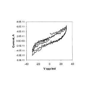
Fig. 7 depicts I-V curves for Sample 3 spin-coated on IDE as prepared and
after
heating in vacuum to 375 K.
CA 02790520 2012-08-20
WO 2011/137508
PCT/CA2011/000490
Description of Preferred Embodiments
Strong interactions between side chains and Tr-faces of asphaltenic systems
explain the tendency for strong self-association and the difficulties in their
characterization. While such non-covalent interactions are detrimental for
bitumen
processing, they are at the same time responsible for favorable interactions
in substances
used for organic electronic devices. Strong Tr-stacking interactions between
polyaromatic
systems is a highly desirable property of organic electronic systems because
such
overlap allows for facile transport of electrons or holes (Newman 2004).
Native asphaltenes are not good conductors (Sill GA, Yen IF. (1969) Fuel 48,
61-74.),
and are therefore not suitable as organic electronic materials. The inventors
have verified
this by using an interdigitated electrode (IDE) device. However, components of
asphaltenes, for example as disclosed vide infra, should display physical and
electronic
characteristics, viz., strong, non-covalent Tr-stacking and large orbital
splittings; indicative
of excellent organic electronic materials. Such components can be separated by
the
methodology described vide infra. Using dispersion-corrected density-
functional theory to
calculate the structures for strongly interacting asphaltene components, it
has now been
shown in the present invention that these asphaltene models (Scheme 1) exhibit
large
orbital splittings which are comparable to known electronic materials such as
polythiophene and pentacene.
The following examples show experimentally that isolated asphaltene components
do indeed act as organic electronic materials, contrary to previous art.
-00
400.
000
100
SOO
Scheme 1 - Model asphaltene components A, B and C form an interacting
aggregate.
Calculation Methodology:
The inclusion of long-range dispersion in density-functional theory DFT
(Johnson ER,
Mackie ID, DiLabio GA. (2009a) J. Phys. Org. Chem. 22, 1127-1135) now allows
for the
6
CA 02790520 2012-08-20
WO 2011/137508
PCT/CA2011/000490
modeling of very large systems, such as asphaltenes. Recently it has been
shown that
dispersion-correcting potentials (DCPs) (DiLabio GA. (2008) Chem. Phys. Lett.
455, 348-
353; Johnson ER, DiLabio GA. (2009b) J. Phys. Chem. C. 113, 5681-5689) can be
used
to correct the long-range behavior of many DFTs, including the B971 and PBE
functionals. These methods are used to calculate the non-covalent interactions
between
asphaltene monomers and/or fragments. In this method, DCPs (simple, atom-
centered
potentials that can be included as input to many programs) correct the long-
range
behavior in weakly bonded systems (Mackie ID, DiLabio GA. (2008) J. Phys.
Chem. A.
112, 10968-10976). Carbon DCPs were used with the Gaussian program (Frisch MJ,
et
al. (2004) Gaussian 03, Revision D.01. (Gaussian Inc., Pittsburgh PA).) in the
present
work to correct the long-range behavior.
The splitting-in-dimer approach (Bredas J-L, Beljonne D, Coropceanu V, Cornil
J.
(2004) Chem. Rev. 104, 4971-5003) is also used to show that well rr-stacked
asphaltenic
models have orbital band widths which may reflect very large charge
mobilities. This
approach can be described as follows: The orbital splitting, SHOMO, defined as
the energy
separation between the highest occupied molecular orbital (HOMO) and the HOMO-
1,
reflect the Marcus-theory transfer integral associated with hole transport.
SLuM0, the
energy separation between the lowest unoccupied molecular orbital (LUMO) and
the
LUM0+1, likewise reflects the transfer integral associated with electron
transport. Using
this simple technique in combination with structures obtained using DFT-DCP
approaches allows assessment of the electronic properties of asphaltene-type
materials.
Vura-Weis et al. have very recently applied a similar combination of
approaches to study
stacked perylenebisimides (Vura-Weis J, Ratner MA, Wasielewski MR. (2010) J.
Am.
Chem. Soc. 132, 1738-1739).
Example 1: Example Model of Asphaltene Components
Calculations were performed on an asphaltene model shown in Scheme 1 (ABC,
C1251-1132N203S3). This molecular formula is derived from experimental 11-I
and 13C NMR,
and from mass spectroscopy measurements (Takonahashi T, Sato S, Tanaka R.
(2004)
Petr. Sci. Tech. 22, 901-914). Previous modeling work has been done under the
assumption that the components aggregate around an open, central structure of
A
(Stoyanov SR, Gusarov S, Kovalenko A. (2008) Mol. Sim. 34, 953-960). This
central
structure should have a folded form in which the two heterocyclic polyaromatic
moieties of
A can maximize their stability by Tr-stacking. Optimization calculations using
PBE/6-
31+G(d,p) with DCPs on an open and folded form confirmed this, predicting that
the
folded form of the aggregate (see Fig. 1) is more stable than the open form by
about 9
7
CA 02790520 2012-08-20
WO 2011/137508
PCT/CA2011/000490
kcal/mol. NMR work lends support for a closed form for asphaltenes similar to
that in Fig.
1.
It is not straightforward to apply the splitting-in-dimer approach to an
aggregate of
molecules. Nevertheless, some insight into the potential for charge transport
may be
gained by applying this approach to ABC. The orbital splitting was calculated
for the
structure of A optimized within the aggregate structure shown in Fig. 2. This
gives SHomo
and Sumo values of 140 and 244 meV, respectively, and indicates that this
moiety may
have substantial ambipolar transport characteristics. Assessing orbital
splittings between
components of the full aggregate (ABC) gives large occupied orbital splittings
between
asphaltene components, viz., S(AB) = 121 and S(AC) = 536 meV, the latter value
pointing to the possibility for significantly large hole transport.
Therefore, the theoretical results support the contention that a component of
asphaltenes has electronic structure properties desirable in organic
electronic materials.
Example 2: Experimental Asphaftene Isolation Procedure (Dettman HD, Inman A,
Salmon
S, Scott K., Fuhr, B. (2005) Energy Fuels 19, 1399-1404.)
Asphaltenes were precipitated from the D1160 vacuum residues [boiling point
(bp)
+524 C1 of global crude oils with pentane, using a single treatment of the
procedure
outlined in Peramanu et. al (Peramanu S, Pruden BP, Rahimi P. (1999) Ind. Eng.
Chem.
Res. 38, 3121-3130.). This method includes adding 40-volumes of pentane,
sonicating in
a bath sonicator for 45 min, leaving the mixture to rest overnight at room
temperature,
then sonicating for an additional 30 min before filtering, and washing with
pentane until
the eluent is colorless. Trace pentane was removed from the asphaltenes
precipitate by
heating the asphaltenes to 45 C in a vacuum oven overnight.
Gel permeation chromatography was run on the asphaltenes using BiobeadsTM S-
X1 purchased from Bio-Rad. These beads are reported to have a molecular weight
separation range from 600 to 14,000 g/mol and comprise styrene divinylbenzene
beads
with 1% crosslinkage and a 40-80 pm bead size. Two 4-ft columns (volume of
approximately 580 mL each) were prepared using beads suspended in
tetrahydrofuran.
The columns were connected in series and were washed with three bed volumes of
chloroform (void volume was approximately 190 mL). The pump flow rate was set
to 0.7
mL/min for all runs with a pressure of 3 psi measured. (SX-1 beads can
withstand
pressures up to 100 psi). It was found that the elution rate was not constant
for all
samples and so fraction volumes were measured at regular intervals to be able
to
8
CA 02790520 2012-08-20
WO 2011/137508
PCT/CA2011/000490
standardize elution profiles by volume rather than by time. For each run,
approximately 2
g of asphaltene sample was dissolved in 5 mL of chloroform and was sonicated
in a bath
sonicator for at least 1 h to homogenize. Fractions were collected in 20-mL
test tubes
using an LKB fraction collector, taking 30 h to complete. A typical elution
profile for
Athabasca bitumen asphaltenes is shown in Fig. 2. Fractions were dried under
nitrogen
in a TurboVapTm evaporator with water bath temperature at 45 C. Fractions were
then put
in a vacuum oven at 45 C overnight before final weights were measured.
Asphaltene Characterization:
Fig. 2 indicates that two physically different types of samples were isolated.
That
which is eluted in the first few fractions (i.e. within the void volume of the
column)
possesses a graphitic texture (including the fractions labeled A & B). By
fraction C the
samples possess an elastic texture. The ratio of the latter (elastic textured
components)
to the former (graphitic textured components) was in the range of 40:60 wt%.
Similar
ratios were obtained for pentane asphaltenes isolated from heavy crude oils
originating
from both South America and the Middle East. The retention of the asphaltene
components, viz., fraction C and longer, are characteristic of those
components with the
desired conductive properties. Note, however, that retention is dependent on
the type of
column employed, how it is packed and with what material it is packed.
Example 3: Asphaltene Experimental Conductance Measurements
Three samples of C5 native asphaltene were studied for their electrical
conductive
properties ¨ Sample 1 consisted of native asphaltene, without component
separation;
Sample 2 consisted of the early asphaltene fraction (A & B), as acquired from
the
procedure outlined above; and Sample 3 consisted of the later eluent
asphaltenes. The
procedure of measuring conductance can be described as thus:
Asphaltene was dissolved in 2 mL of toluene; the sample spin-coated (1000 rpm
for 65 seconds) on a lithography-patterned inter-digitated electrode (IDE, 10
tirn
separation and 600 digits) on p-Si substrate with 300 nm thermal oxide as an
insulating
layer. The height of the IDE was 105 nm, constituted by 5 nm Cr (adhesion
layer) and
100 nm Au. The sample was dried under vacuum (2 x 10⁻⁶ torr) for 24 hours,
with all
experimental data collected under vacuum, and in darkness.
In order that the resistivity of the sample can be determined, the thickness
of the
sample must be measured. Sample thickness was measured by an atomic force
microscopy (AFM) scratching technique (Anariba F, DuVail SH, McCreery RL.
(2003)
9
CA 02790520 2012-08-20
WO 2011/137508
PCT/CA2011/000490
Anal. Chem. 75, 3837-3844.), whereby an AFM cantilever is used in contact mode
with a
force high enough to scratch away the spin coated layer but not scratch into
the Si02
layer. After scratching, the same AFM cantilever is used to image the
scratched region in
tapping mode. The depth of the layer is determined by the height difference
between the
unscratched and scratched regions.
For the IDE device spin-coated with Sample 3, contact mode was used to scratch
a
trench 4 pm x 4 pm between two digits (10 pm separation). In tapping mode, an
8 pm x 8
pm area, including the scratched region, was imaged. The measured thickness
was
135.6 3.2 nm, see Fig. 3. The conductance was determined by measuring
current as a
function of applied voltage by making contact to each "macro" terminal of the
IDE device.
Asphaltene Experimental Conductance Data:
The measured experimental data can be summarized as follows:
1. Native asphaltene shows no conductive properties, confirming the
conclusions of
Sill, who showed that doping by iodine was necessary in order to make
asphaltene
conductive (Sill 1969).
2. Sample 2 was measured as non-conductive. This suggests the need for further
processing and/or different deposition techniques to make the early separated
asphaltene
fraction operative as an organic electronic material.
3. At ambient temperature, Sample 3 shows improved conductance over
anthracene,
measured using the same procedure, see Fig. 4. Resistivity measurements of ca.
4.9 x
1012 acm (asphaltene) and ca. 4.56 x 10¹³ acm (anthracene) were obtained. Such
data
are sensitive to noise conditions, but the asphaltene data is based upon an
average of 9
different measurements on the same sample. Furthermore, statistical analysis
using the
paired t student (2-tails) test indicates significant difference between bare
IDE and IDE-
Sample 3, with 95 % confidence.
4. Fig. 5 shows an overlay of 3 different measurements, indicating that the
electrical
behavior of Sample 3 is reproducible.
5. Setting the same Sample 3 as used for (3) in ambient atmosphere for 2 weeks
resulted in increased conductance (by ca. 3 orders of magnitude). Such a
response is
common to many known organic electronic materials, possibly as a result of
water or
oxygen impurities, or from the effects of UV radiation. However, Fig. 6
suggests that the
WO 2011/137508
PCT/CA2011/000490
structure of the asphaltene component can support charge, and therefore that
the sample
can be gated.
6. Qualitatively similar results as for (5) were obtained upon heating Sample
3 to 375
K; the current increased by about one order of magnitude, as shown in Fig. 7.
This
temperature effect is reversible upon sample cooling, suggesting that an
activated
conductivity phenomenon is in effect. Furthermore, this indicates that the
sample shows
semiconductor behavior rather than metallic.
The present invention includes asphaltene components having the desired
properties to make excellent organic electronic devices. Advantages over known
molecules in the art (e.g., rubrene, pentacene, tetracene, and polythiophenes)
include
making use of an already synthesized chemical, with only simple separation
required
from what is an air stable species. Turning what was previously thought of as
a waste
product into a useful device can also be considered advantageous.
Other advantages that are inherent to the structure are obvious to one skilled
in
the art. The embodiments are described herein illustratively and are not meant
to limit
the scope of the invention as claimed. Variations of the foregoing embodiments
will be
evident to a person of ordinary skill and are intended by the inventors to be
encompassed
by the following claims.
11
CA 2790520 2017-07-20