Note : Les descriptions sont présentées dans la langue officielle dans laquelle elles ont été soumises.
METACAPACITORS AND POWER-ELECTRONIC CONVERTERS FOR POWER-
ELECTRONIC SYSTEMS
CROSS-REFERENCE TO RELATED APPLICATIONS
This application claims the benefit of US Provisional Patent Application
Serial
No. 62/914,237, filed October 11,2019.
FIELD OF THE DISCLOSURE
The present disclosure relates generally to power-electronic systems and
components
thereof, and in particular to high-density energy-storage apparatuses using
supercapacitors for
providing energy storage, and power-electronic apparatuses and methods using
direct power
transfer for converting power from one form to another.
BACKGROUND
Power-electronic apparatuses and systems provide solutions to power various
power-
consumption loads such as electronic devices and, if needed, convert power
from one form to
another for powering the loads. Almost all devices involving the use of
electricity utilize some
power-electronics technologies. The power-electronic apparatuses and systems
usually involve
and power-electronic circuitries such as power converters.
The power sources usually comprise power generators, energy-storage
apparatuses and
systems, and related circuitries. The power generators may be traditional
thermal power station
using generating electricity using fossil fuel (e.g., coal, natural gas,
and/or oil), and/or power
generators using renewable energy such as wind power, solar power, and/or the
like.
Renewable energy is a clean and practical power-generation method for
providing
electrical power to end-users. For example, rooftop solar panels have gained a
lot of attention to
fulfill residential energy demand. Wind energy has been used for harvesting
wind power and
generate electricity. Solar and wind have been amongst the fastest growing
renewable energy
systems due to their prominent advantages.
While renewable energy may become one of the mainstream energy-generation
technologies in the future, there still exist many challenges that impede the
widespread adoption
of renewable-energy technologies. Some of these challenges include:
= the energy generation may not be reliable due to the intermittency of
solar and
wind;
1
Date Recue/Date Received 2021-11-12
CA 03122602 2021-06-09
WO 2021/068085
PCT/CA2020/051366
= there is a wide range of variations in the operating points of solar/wind
energy
harvesting systems, which may significantly degrade the overall efficiency of
the system; and
= the energy harvesting systems usually need the utility grid in order to
provide
resiliency.
Due to the aforementioned challenges, the existing solar/wind energy
harvesting systems
may not provide an optimal solution for many emerging applications.
Considering the exponential
growth of solar/wind energy systems and their impacts on the landscape of
energy harvesting
systems, sub-optimal operation significantly affect these systems in an
adverse manner.
Energy-storage systems may provide a solution for overcoming the
aforementioned
challenges of intermittent renewable-energy sources and facilitate a reliable
renewable-energy
harvesting system.
Energy-storage systems often comprise one or more batteries for storing
energy. For
example, Lithium-Ion batteries have been used in many applications (e.g.,
electric vehicles,
residential energy storage, laptops, smart phones, tablets, and the like).
Other types of battery
technologies such as redox-flow batteries have also been used in some
applications (e.g., grid-
scale energy storage).
Batteries are mostly based on some kinds of redox reactions. Thus, they
usually suffer
from volumetric modulation and swelling of active materials (usually due to
the excessive redox
reactions) during charge and discharge cycles. In general, when there are
electro-chemical
reactions, there will be degradation and reduced number of life cycles.
Although there has been
substantial research on mitigating the degradation to provide extended
lifetime, the lifetime of
existing batteries is still limited. In addition, high-performance batteries
usually require expensive
and unsafe materials which may be flammable and have several safety risks.
Other drawbacks of batteries include that batteries are usually bulky and that
batteries
usually have low power density.
Supercapacitors have been presented as another contender for energy-storage
markets. As
those skilled in the art will appreciate, supercapacitors may provide
substantial energy-storage
capacity and offer improved performance particularly in terms of life-time and
dynamics,
compared to the battery technologies. For example, electric double-layer
capacitors (EDLCs) are
merely based on creation of an electric field with virtually no chemical
reactions. Thus, EDLCs
may provide very long lifetime (e.g., up to millions of charge/discharge
cycles) and very high
power density.
While the power density of supercapacitors is usually hundreds of times (e.g.,
100-1000
times) higher than that of batteries, the energy density (volumetric energy
density measured in
Wh/Litre) or gravimetric energy density measured in Wh/Kg) of supercapacitors
is relatively
2
CA 03122602 2021-06-09
WO 2021/068085
PCT/CA2020/051366
limited. For example, the energy density of batteries is usually tens of times
(e.g., 3-30 times)
higher than that of supercapacitors. In fact, the low energy density of
supercapacitors may be the
main reason that batteries are much more prevalent in mainstream energy
storage despite
tremendous advantages offered by supercapacitors.
Thus, existing energy-storage systems are usually bulky (e.g., due to their
low energy-
density), and usually have short life-span, low capacity, and costly.
Therefore, there is a need for
high-density energy-storage systems with low cost. Such high-density energy-
storage system may
not only revolutionize the future of energy systems, but may also be used in
many other
applications such as biomedical (e.g., wearable devices, implants, and/or the
like), robotics,
Internet-of-Things (loT) devices, and the like.
With respect to power-electronic circuitries of the power-electronic
apparatuses and
systems, power-electronics technologies and power-electronic converters have
been used for
many applications such as renewable energy systems, energy storage systems,
electric vehicles,
electronic devices (e.g. smart phones, tablets, and the like), and LED
lighting. Thus, power-
electronic converters play a critical role in energy systems and electronic
devices. Power-
electronic converters and their applications have exhibited an exponential
growth.
The efficiency, power density, and reliability of power-electronic converters
are of great
importance for various applications. However, there exit various challenges
and difficulties
related to prior-art power conversion technologies, such as:
high amount of switching losses due to hard switching of power semiconductors;
=
= high amount of conduction losses in various components used in the power
circuitry; and
= difficulties in thermal management for removing heat generated during
operation
of power-electronic converters while ensuring reliable operation thereof.
Due to these challenges, the prior-art power-electronic converters may not
provide
sufficiently high or even optimal efficiency. Because of the wide use and
exponential growth of
power-electronic converters and their applications, any sub-optimal
performance or inefficiency
thereof may cause significant energy waste and consequently significant
detrimental-impacts to
global environment.
Therefore, there is a need for highly efficient power-electronic converters
for solving the
above-described issues and challenges.
3
CA 03122602 2021-06-09
WO 2021/068085
PCT/CA2020/051366
SUMMARY
According to one aspect of this disclosure, there is provided an ultra-high
density energy-
storage apparatus and system with high lifetime (e.g., in the range of
hundreds of thousands cycles)
and very high energyipower density.
According to one aspect of this disclosure, there is provided an electrical-
energy storage
device comprising: a conductive or semi-conductive first metasurface layer; a
conductive or semi-
conductive second metasurface layer; and a dielectric layer sandwiched between
the first and the
second metasurface layers for electrically insulating the first metasurface
laver from the second
metasurface layer.
In some embodiments, the first metasurface layer comprises a plurality of nano-
scale or
micro-scale first structures; the second metasurface layer comprises a
plurality of nano-scale or
micro-scale second structures; and the first and the second structures
extending into each other
without electrical contact therewith.
In some embodiments, the first structures comprise a plurality of recesses at
distal ends
thereof; and at least a second set of the second structures are received in
the recesses of the first
structures without electrical contact therewith.
In some embodiments, the first structures comprise a plurality of first rods
having recesses
at distal ends thereof; and at least a portion of the second structures are
received in the recesses of
the first rods without electrical contact therewith.
In some embodiments, the first structures comprise a plurality of first rods;
and the second
structures comprise a plurality of second rods interleaved with the first
rods.
In some embodiments, at least a first set of the first and the second
structures has a circular,
elliptical, or rectangular cross-section.
In some embodiments, one or more dimensions of each of the first and the
second
structures are in a nanometer range or in a micrometer range.
In some embodiments, the thicknesses of the first and the second structures
are in the
nanometer range or in the micrometer range.
In some embodiments, the electrical-energy storage device further comprising
at least one
of: a first electrode coupled to the first metasurface layer; and a second
electrode coupled to the
second metasurface layer.
In some embodiments, at least one of the first and the second metasurface
layers comprises
an electrically conductive base forming an electrode.
According to one aspect and in some embodiments, there is provided a method of
fabricating an electrical-energy storage device; the method comprises: (i)
depositing a first
conductive layer onto a substrate; (ii) spin-coating a photoresist layer onto
the conductive layer;
4
CA 03122602 2021-06-09
WO 2021/068085 PCT/CA2020/051366
(iii) applying a mask to the photoresist layer and exposing the masked
photoresist layer under a
light, the mask having a predefined pattern; (iv) removing the un-exposed part
of the photoresist
layer with development; (v) depositing a first conductive material to the
photoresist layer for
allowing the conductive material to fill the removed part of the photoresist
layer; (vi) dissolving
the photoresist layer for forming a first set of conductive structures; (vii)
depositing a layer of a
dielectric material to the deposited first conductive material for forming a
dielectric layer thereon;
(viii) depositing a second conductive material to the dielectric layer forming
a second set of
structures, and (ix) electroplating a third conductive material to the second
set of structures.
In some embodiments, the substrate is silicon (Si).
In some embodiments, the first conductive layer comprises silver (Ag).
In some embodiments, the first conductive layer further comprises titanium
(Ti).
In some embodiments, the photoresist layer comprises SU-8.
In some embodiments, the light comprises an ultraviolet (UV) light.
In some embodiments, the first conductive material comprises Ag.
In some embodiments, the dielectric material comprises fused silica (SiO2).
In some embodiments, the second conductive material comprises Ag.
In some embodiments, the third conductive material comprises Ag.
According to one aspect and in some embodiments, there is provided a power-
electronic
conversion system and power-electronic converter using direct power transfer
(DPT). The power-
electronic converter disclosed herein may provide highly efficient and
reliable solutions for
various applications.
According to one aspect and in some embodiments, there is provided an
electrical power
conversion apparatus comprising: a first power conversion circuitry for
receiving an input current
from an electrical power source, converting a first portion of electrical
power of the input current,
and outputting the converted electrical power via at least one output. the
first power conversion
circuitry comprising a first transformer having a primary side for coupling to
the electrical power
source and a secondary side for coupling to the at least one output; and at
least one direct power
transfer (DPT) channel electrically coupling to the first power conversion
circuitry in parallel for
bypassing the first power conversion circuitry and directly transferring a
second portion of the
electrical power received from the electrical power source to the secondary
side of the first
transformer for power-outputting via the at least one output.
In some embodiments, the first power conversion circuitry comprises a current-
switching
structure coupling to the primary side of the first transformer for switching
current.
In some embodiments, the at least one DPT channel is coupled to the primary
side of the
first transformer via a second transformer.
5
CA 03122602 2021-06-09
WO 2021/068085
PCT/CA2020/051366
In some embodiments, the first and second transformers share a common core.
In some embodiments, the first power conversion circuitry comprise at least a
pair of
power semiconductors Siand S2 adapted for operation under a zero-voltage
switching (ZVS)
condition.
In some embodiments, the at least first and second power semiconductors
comprise at least
one pair of metal-oxide-semiconductor field-effect transistors (MOSFETs).
In some embodiments, the apparatus further comprises a plurality of output
diodes adapted
for operation under a zero-current switching (ZCS) condition.
In some embodiments, the apparatus further comprises an input switch for
coupling the
electrical power source to the first power conversion circuitry and the at
least one DPT channel;
the plurality of output diodes comprises four diodes D1, D2, D3, and D4; a
first end of Di is coupled
to a first end of D2 forming a first input end, and a first end of D3 is
coupled to a first end of D4
forming a second input end, the first and second input ends are coupled to the
secondary side of
the first transformer and an output side of the at least one DPT channel; a
second end of Di is
coupled to a second end of D3 forming a first output end, and a second of D2
is coupled to a second
end of D4 forming a second output end, the first and second output ends are
coupled to the at least
one output; and the apparatus is adapted for operation in a plurality of modes
comprising: (i) a
first mode in which Di and D4 are ON, and Si is switched from ON to OFF under
the ZVS
condition, (ii) a second mode in which Di and D4 are ON, and S2 is switched ON
under the ZVS
condition, (iii) a third mode in which Di and D4 turn OFF, D2 and D3 turn ON
under the ZCS
condition, and S2 is ON, (iv) a fourth mode in which S2 is switched OFF under
ZVS condition, (v)
a fifth mode in which Si is switched ON under ZVS condition, and D2 and D3 are
ON, (vi) a sixth
mode in which D2 and D3 turn OFF under ZCS condition, Di and D4 turn ON under
ZCS condition,
and (vii) a seventh mode in which the input switch turns off for turning the
input current to zero.
In some embodiments, the input switch is a diode.
In some embodiments, the apparatus is adapted for operating the input current
in a pseudo-
continuous conduction mode (pseudo-CCM) for reducing the peak and/or root-mean-
square (RMS)
values thereof
In some embodiments, the first power conversion circuitry comprises a first
resonant tank.
In some embodiments, the at least one DPT channel comprises at least one
second resonant
tank.
In some embodiments, the input current is an alternate current (AC) or a
direct
current (DC).
In some embodiments, the at least one output comprises an AC output or a DC
output.
6
CA 03122602 2021-06-09
WO 2021/068085 PCT/CA2020/051366
In some embodiments, the at least one output comprises a plurality of outputs;
the at least
one DPT channel comprises a plurality of DPT channels; and at least two of the
plurality of DPT
channels are coupled to different ones of the plurality of outputs.
BRIEF DESCRIPTION OF THE DRAWINGS
The embodiments of the present disclosure will now be described with reference
to the
following figures in which identical reference numerals in different figures
indicate identical
elements, and in which:
FIG. 1 is a schematic diagram showing the basic operation of a traditional
capacitor;
FIG. 2 is a schematic diagram showing the basic structure of an electric
double-layer
capacitor (EDLC);
FIG. 3A is a schematic diagram showing a carbon nano-tube (CNT) based EDLC;
FIG. 3B is a schematic diagram showing a graphene-based EDLC;
FIG. 4 is a schematic diagram of a supercapacitor, according to some
embodiments of this
disclosure;
FIG. 5A is a schematic diagram of a supercapacitor, according to yet some
embodiments
of this disclosure;
FIG. 5B is a schematic diagram showing the cylindrical nano/micro structures
of the
supercapacitor shown in FIG. 5A;
FIG. 5C is a schematic diagram showing the cubical nano/micro structures of
the
supercapacitor shown in FIG. 5A;
FIG. 6A is a schematic diagram of a supercapacitor, according to still some
embodiments
of this disclosure;
FIG. 6B is a schematic diagram of a supercapacitor, according to some
embodiments of
this disclosure;
FIG. 7A is a perspective view of a supercapacitor, according to yet some
embodiments of
this disclosure;
FIG. 7B is a perspective cross-sectional view of the supercapacitor shown in
FIG. 7A along
the cross-sectional plane A-A; and
FIG. 7C is an exploded perspective view of the supercapacitor shown in FIG.
7A;
FIGs. 8A to 8K illustrate a process of fabricating the supercapacitor shown in
FIG. 7A,
according to some embodiments of this disclosure;
FIG. 9 is a schematic diagram showing an exemplary arrangement of a DC micro-
grid;
FIGs. 10A to 10D are schematic diagrams of a power-electronic conversion
system
according to some embodiments of this disclosure, wherein
7
CA 03122602 2021-06-09
WO 2021/068085
PCT/CA2020/051366
FIG. 10A shows the power-electronic conversion system having an alternate-
current (AC) power source, a direct-current (DC) load, and an AC-to-DC (AC/DC)
power
converter therebetween.
FIG. 10B shows the power-electronic conversion system having a DC power
source, a DC load, and a DC-to-DC (DC/DC) power converter therebetvveen,
FIG. 10C shows the power-electronic conversion system having a DC power
source, an AC load, and a DC-to-AC (DC/AC) power converter therebetween, and
FIG. IOD shows the power-electronic conversion system having an AC power
source, an AC load, and an AC-to-AC (AC/AC) power converter therebetween;
FIG. 11 is a schematic diagram of the circuitry of a prior-art resonant DC/DC
converter
for using in the power-electronic conversion system shown in FIG. 10B;
FIG. 12 is a schematic diagram of the circuitry of a prior-art non-resonant
DC/DC
converter for using in the power-electronic conversion system shown in FIG.
10B;
FIG. 13 is a schematic diagram of the circuitry of an AC/DC converter for
using in the
power-electronic conversion system shown in FIG. 10A;
FIG. 14 is a schematic diagram of the circuitry of the prior-art non-resonant
DC/DC
converter shown in FIG. 12 with block arrows showing the power flow for
indicating that the
power semiconductors thereof process all input power;
FIG. 15 is a schematic diagram of a power-electronic conversion system using
direct
power transfer (DPT), according to some embodiments of this disclosure, the
power-electronic
conversion system comprising a power-electronic converter having a power-
conversion circuitry
and a DPT channel electrically coupled together in parallel;
FIG. 16A is a schematic diagram of the circuitry of a DC/DC converter shown in
FIG. 15,
according to some embodiments of this disclosure;
FIGs. 16B to 161-I show different operation modes of the DC/DC converter shown
in FIG.
16A;
FIG. 17 shows the key waveforms of the DC/DC converter shown in FIG. 16A;
FIG. 18 is a schematic diagram showing a simplified circuit of the DC/DC
converter shown
in FIG. 16A;
FIG. 19 shows the plot of a parameter P
- DPT,n of the DC/DC converter shown in FIG. 16A
in terms of different values of n4 and nf of the DC/DC converter shown in FIG.
16A;
FIG. 20 shows the plot of the inductances L1, L2, and M of the DC/DC converter
shown in
FIG. 16A in terms of the coupling coefficient k.
FIGs. 21A to 21F show the simulation results of the DC/DC converter shown in
FIG. 16A
at the nominal load, wherein
8
CA 03122602 2021-06-09
WO 2021/068085
PCT/CA2020/051366
FIG. 21A show the waveforms of the switch Si,
FIG. 21B shows the waveforms of the switch S2,
FIG. 21C shows the current waveforms of the coupled inductor,
FIG. 21D shows the waveforms of vin, Ypriin, and it.,
FIG. 21E shows the waveforms of vsee and it, and
FIG. 21F shows the current and voltage waveforms of the output diodes Di and
D2;
FIG. 22 is a photograph of the prototype of the DC/DC converter shown in FIG.
16A;
FIGs. 23A to 23F show the experimental waveforms obtained from the prototype
shown
in FIG. 22 under the full-load condition;
FIGs. 24A to 24F show the experimental waveforms obtained from the prototype
shown
in FIG. 22 at 50% of the nominal power;
FIG. 25 shows the efficiency measured from the prototype shown in FIG. 22 from
20%
to 100% of the rated power;
FIG. 26 is a schematic diagram of the circuitry of an AC/DC power-electronic
converter
shown in FIG. 15, according to some embodiments of this disclosure;
FIG. 27 is a schematic diagram of the circuitry of a DC/DC power-electronic
converter
shown in FIG. 15, according to some embodiments of this disclosure, the power-
conversion
circuitry thereof comprising a resonant tank;
FIG. 28 is a schematic diagram of the circuitry of a DC/DC power-electronic
converter
shown in FIG. 15, according to some embodiments of this disclosure, the DPT
channel thereof
comprising a resonant tank:
FIG. 29 is a schematic diagram of the circuitry of a DC/DC power-electronic
converter
shown in FIG. 15, according to some embodiments of this disclosure, each of
the power-
conversion circuitry and the DPT channel thereof comprising a resonant tank;
FIG. 30 is a schematic diagram of the circuitry of an AC/DC power-electronic
converter
shown in FIG. 15, according to some embodiments of this disclosure, the power-
conversion
circuitry thereof comprising a resonant tank;
FIG. 31 is a schematic diagram of the circuitry of an AC/DC power-electronic
converter
shown in FIG. 15, according to some embodiments of this disclosure, the DPT
channel thereof
comprising a resonant tank:
FIG. 32 is a schematic diagram of the circuitry of an AC/DC power-electronic
converter
shown in FIG. 15, according to some embodiments of this disclosure, each of
the power-
conversion circuitry and the DPT channel thereof comprising a resonant tank;
FIG. 33 is a schematic diagram of the circuitry of a DC/DC power-electronic
converter
shown in FIG. 15, according to some embodiments of this disclosure, the power-
conversion
9
CA 03122602 2021-06-09
WO 2021/068085
PCT/CA2020/051366
circuitry and the DPT channel thereof comprising transformers sharing a common
magnetics
structure with coils separately wound on a common core;
FIG. 34 is a schematic diagram of the circuitry of a DC/DC power-electronic
converter
shown in FIG. 15, according to some embodiments of this disclosure, the power-
conversion
circuitry and the DPT channel thereof comprising transformers sharing a common
magnetics
structure implemented as a center-tap transformer;
FIG. 35 is a schematic diagram of a power-electronic conversion system using
DPT,
according to some embodiments of this disclosure, the power-electronic
conversion system
comprising a power-electronic converter having a power-conversion circuitry
and a plurality of
DPT channels electrically coupled together in parallel;
FIG. 36 is a schematic diagram of the circuitry of an exemplary DC/DC
converter shown
in FIG. 35, according to some embodiments of this disclosure, the power-
electronic conversion
system comprising a power-electronic converter having a power-conversion
circuitry and two
DPT channels electrically coupled together in parallel;
FIG. 37 is a schematic diagram of a power-electronic conversion system using
DPT,
according to some embodiments of this disclosure, the power-electronic
conversion system
comprising a multiple-output power-electronic converter having a power-
conversion circuitry and
a plurality of DPT channels electrically coupled together in parallel; and
FIG. 38 is a schematic diagram of the circuitry of an exemplary multiple-
output DC/DC
converter shown in FIG. 37, according to some embodiments of this disclosure,
the power-
electronic conversion system comprising a power-electronic converter having a
power-conversion
circuitry and two DPT channels electrically coupled together in parallel.
DETAILED DESCRIPTION
Embodiments herein relate to power-electronic systems and components thereof
such as
energy-storage apparatuses/subsystems in the form of supercapacitors and power-
electronic
apparatuses/subsystems.
Supercapacitors
According to one aspect and in some embodiments, there is provided a
supercapacitor with
substantially increased energy density which may surpass that of batteries.
The supercapacitor
structure disclosed herein may bring supercapacitor technology to the
forefront for energy-storage
markets.
FIG. 1 shows the basic operation of a traditional capacitor 10 which comprises
a pair of
electrodes 12 with a layer of dielectric material 14 sandwiched therebetween.
Electrical power is
.. output from the electrodes 12 via conductors 16 for powering a load 18.
CA 03122602 2021-06-09
WO 2021/068085
PCT/CA2020/051366
According to FIG. 1, the capacitance of the capacitor 10 is given by:
A (1)
C = E ¨
d
where C is the capacitance (in Farad), E is the electric filed permittivity of
the dielectric material 14
(which is a constant), A is the area of the overlap between the two electrodes
12 (in m2), and d is
the distance between the electrodes 12 (in meter). One may also use
centimeters (cm) instead of
meters for distance d in some embodiments.
The energy stored in the capacitor 10 is given by:
1 1A (2)
W = ¨2CV2 = ¨2e ¨dV2
where V is the voltage (in Volt) applied to the electrodes 12 (using the
aforementioned units, the
energy W is in Joules)
The equation (2) of energy indicates the parameters that affect the energy
density of the
capacitor 10. These parameters are:
= overlapping area A between the two electrodes 12;
= distance d between the electrodes 12;
= electric field permittivity of the dielectric 14; and
= Operating voltage V of the capacitor 10.
With simple structures similar to that shown in FIG. 1, the capacitance C and
stored energy
W are often far too small to make the capacitors 10 a viable option for energy
storage purposes.
In prior art, much effort has been done to optimize the aforementioned
parameters and increase
the energy density of capacitors (which may then be denoted
"supercapacitors").
FIG. 2 shows the basic structure of an electric double-layer capacitor (EDLC)
20. In this
structure, the electrodes (i.e., the anode 22 and cathode 24) are spaced apart
by a separator 26
(such as a membrane) with electrolyte 28 sandwiched between the electrode 22,
24 and the
separator 26. The EDLC 20 stores energy through charge separation (the same
mechanisms as the
traditional capacitors 10 shown in FIG. 1). As can be seen, the structure of
the EDLC 20 is
symmetrical and may provide alternative polarity. The main energy is stored in
the electric filed
between the two electrodes 22 and 24. The stronger the electric field, the
more energy stored in
the EDLC 20.
As shown in FIG. 2, the EDLC 20 comprises two separated charge layers 30 at
the interface
between the electrolyte 28 and the positive/negative electrodes 22 and 24
(hence the name electric
double-layer capacitor). This is unlike the traditional structures which only
comprises a single
layer charge separation. In EDLCs 20, the distance between electrical double
layers 30 is much
smaller than that of traditional structures 10. Thus, the capacitance and in
turn the stored energy
may be increased by several orders of magnitude compared those of traditional
structures 10.
11
Area and distance are the main parameters that may be controlled to achieve
high capacity
and high energy density for EDLCs 20. As high specific surface area is
generally desirable in
EDLCs, high capacity and high energy density may be achieved by using
materials with high
specific surface area and good electrical conductivity such as nano-
structures. Examples of such
nano-structures include carbon nano-tubes (CNTs) and graphene, wherein CNTs
are one-
dimensional (1D) structures and graphene are two-dimensional (2D) structures.
Graphene has
even larger specific surface area compared to CNTs, and therefore has been
used in many EDLC
structures. FIGs. 3A and 3B show the structures of EDLCs with CNTs 30 and
graphene 40,
respectively. As shown, the structures of EDLCs with CNTs 30 and graphene 40
are similar to
that of the EDLC 20 shown in FIG. 2 except that the EDLCs 30 and 40 comprise
CNTs 30 and
graphene 40, respectively, sandwiched between the electrode 22, 24 and the
separator 26.
Although carbon nano-structures may provide high specific surface area and
offer high
number of charge/discharge cycles, there are some challenges to use them for
EDLCs. These
challenges are mainly related to the synthesis and fabrications of carbon nano-
structures for
EDLCs and consistency of the devices. Moreover, despite the fact that carbon
nano-structures
have significantly improved the performance of EDLCs, their energy density may
still be lower
than that of the batteries.
While CNTs and graphene structure effectively increase the specific surface
area and in
turn the capacity, such an increase is somewhat random and cannot achieve the
full theoretical
size of specific surface area. For instance, in theory, graphene should
achieve a specific surface
area of thousands of m2/g (2630 m2/g). However, the practically achieved
specific surface area of
graphene is in the order of tens or at most hundreds of m2/g. The main problem
is stemmed from
the atomic and molecular structures of these nano-structures.
Turning now to FIG. 4, a supercapacitor according to some embodiments of this
disclosure
is shown and is generally identified using reference numeral 100. As shown,
the
supercapacitor 100 comprises a pair of electrode layers 102A and 102B
(collectively identified
using reference numeral 102) and a dielectric layer 104 sandwiched between the
electrode
layers 102. In these embodiments, each electrode layer 102 comprises a
conductive or semi-
conductive metasurface coupled to respective electrode layers 102 for
increasing the specific
surface area, and a suitable dielectric material sandwiched between the
metasurfaces for
electrically insulating the metasurfaces from each other.
The academic paper entitled "LIGHT PROPAGATION WITH PHASE
DISCONTINUITIES: GENERALIZED LAWS OF REFLECTION AND REFRACTION," by
Nanfang Yu, Patrice Genevet, Mikhail A. Kats, Francesco Aieta, Jean-Philippe
Tetienne, Federico
12
Date Recue/Date Received 2021-11-12
Capasso, and Zeno Gaburro, Science volume 334, issue 6054, pages 333-337
(2011), describes
metasurfaces in view of their use in optical field.
The conductive or semi-conductive metasurface used in the supercapacitor 100
disclosed
herein may be similar to those described in the above-mentioned academic paper
but does not
necessarily need to exhibit the optical features described therein.
In particular, the conductive or semi-conductive metasurface used in the
supercapacitor 100 is a structure having a two-dimensional (2D) surface with
superimposed nano-
scale structures (also denoted "nano-structures") arranged with a nano-scale
spacing, wherein the
nano-scale structures are made of one or more suitable electrically conductive
or semi-conductive
materials.
In some embodiments, the nano-scale structures may be structures with one or
more
dimensions thereof being in nanometer (nm) range (e.g., less than 1 micrometer
(pm)), and ``nano-
scale spacing" refers to the spacing between the nano-scale structures is in
nanometer range. In
some embodiments, the nano-scale structures may comprise a plurality of
nanorods (also denoted
"antennas"). In some embodiments, the nano-scale structures 124 may comprise a
plurality of V-
shaped nanorods. The nano-scale structures may form a periodic or repetitive
pattern and each
pattern may comprise a plurality of nano-scale structures of different shapes
and dimensions.
In some embodiments, the metasurface of each electrode layer 102 may comprise
a
plurality of micro-scale structures (i.e., one or more dimensions thereof
being in micrometer range
(e.g., less than 1 millimeter (mm)), and/or with a micro-scale spacing
therebetween.
The supercapacitor 100 disclosed herein may be denoted a "meta-supercapacitor"
or
"metacapacitor". By using the metasurfaces, the effective area is tremendously
enhanced by the
nano/micro structures as the size of these columns/cylinders can be in
nanometer or micrometer
range.
In some embodiments, the nano/micro structures of the metasurfaces of the
electrode
layers 102 extend into each other without electrical contact therewith and
electrically insulated by
the dielectric layer 104 sandwiched therebetween. As the nano/micro structures
of the
metasurfaces have a nano-scale or micro-scale spacing, the distance between
the metasurfaces is
therefore significantly reduced. As a result, the supercapacitor 100 disclosed
herein may provide
ultra-high energy density and offer consistent device performance.
For example, FIG. 5A shows the structure of a supercapacitor 100 in one
embodiment. As
shown, the supercapacitor 100 comprises a pair of electrode layers 102A and
102B and a dielectric
layer 104 sandwiched therebetween.
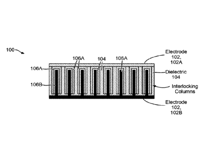
Each electrode layer 102A, 102B comprises a metasurface 106A, 106B
(collectively
identified using reference numeral 106) with nano-structures arranged in
interlocking columns for
13
Date Recue/Date Received 2021-11-12
CA 03122602 2021-06-09
WO 2021/068085 PCT/CA2020/051366
increasing the specific surface area and reducing the spacing therebetween. In
particular, the
electrode layer 102A comprises a first metasurface 106A which comprises a
plurality of first nano-
structures (also identified using reference numeral 106A) in the form of
hollow rods extending
from the 2D surface of the first electrode layer 102A and having open distal
ends (i.e., having
recesses at the distal ends thereof).
The electrode layer 102B comprises a second metasurface 106B which comprises a
plurality of second nano-structures (also identified using reference numeral
106B) in the form of
solid or hollow rods extending from the 2D surface of the second electrode
layer 102B. In
embodiments where the second nano-structures are hollow rods, such hollow rods
may also
comprise open distal ends for further increasing the specific surface area.
In these embodiments, at least some of the second nano-structures 106B are
received in
the recesses of respective first nano-structures 106A without electrical
contact therewith, thereby
forming the interlocking columns. The first and second nano-structures 106A
and 106B are
separated by a suitable dielectric material of the dielectric layer 104 which
separates the electric
charges.
In some embodiments, the interlocking columns 106 may comprise first and
second micro-
structures 106A and 106B with at least some of the second micro-structures
106B received in
respective first micro-structures 106A.
In various embodiments, the first and second nano/micro structures 106A and
106B may
be in any suitable shapes. For example, in some embodiments as shown in FIG.
5B, the first and
second nano/micro structures 106A and 106B may be in cylindrical shapes with a
circular or
elliptical cross-section. In some embodiments as shown in FIG. SC, the first
and second
nano/micro structures 106A and 106B may be in cubical shapes with a
rectangular cross-section.
The supercapacitor 100 disclosed herein may tremendously increase the stored
energy by
substantially increasing the specific surface area (i.e., the effective
overlapping area) and
significantly reducing the distance between electrode layers 102. Compared to
existing EDLCs,
the supercapacitor 100 may fully utilize the surface area such that the
capacitance thereof and in
turn the energy stored therein may be increased by many orders of magnitude.
In above embodiments, the first and the second nano-scale or micro-scale
structures 106A
and 106B extending into each other without electrical contact therewith by
receiving at least some
of the second structures 106B into the recesses of corresponding first
structures 106A.
In some embodiments as shown in FIG. 6A, the first metasurface 106A does not
comprise
any nano-scale or micro-scale rods. Rather, the first metasurface 106A
comprises a plurality of
nano-scale or micro-scale recesses for receiving the nano/micro structures
106B therein without
electrical contact.
14
CA 03122602 2021-06-09
WO 2021/068085 PCT/CA2020/051366
In some embodiments as shown in FIG. 6B, the nano-scale or micro-scale
structures of the
first and second metasurfaces 106A and 106B are interleaved (i.e., one
adjacent another) without
electrical contact.
In above embodiments, each metasurface is formed by depositing the nano/micro
structures on a conductive base wherein the conductive base also acts as an
electrode layer.
Therefore, in these embodiments, additional or separate electrode layers may
not be required. hi
yet some embodiments, each metasurface may be coupled to another electrode
layer and is
electrically conductive therewith.
As described above, the effective surface area of the supercapacitor 100 is
greatly
increased by incorporating nano-rods or nano-pillars into the design of the
electrodes 102. The
nano-pillars may have circular, elliptical, square, or any other shapes
suitable for fabrication. In
order to maintain the small gap between the electrodes 102, the nano-pillars
of one electrode may
have a complementary shape with respect to those of the other electrode. The
dielectric layer
comprises a suitable dielectric material such as SiO2, A1203, or other
dielectric materials with high
breakdown voltages for filling into the gaps between the nano-scale structures
of the
electrodes 102 and electrically insulating them from each other.
The supercapacitor 100 may tremendously increase the stored energy by
substantially
increasing the specific surface area and significantly reducing the distance
between electrodes.
Thus, the impact of the structure of the supercapacitor 100 disclosed herein
is three-fold:
2() Increasing the effective overlapping area,
=
= Decreasing the distance between the electrodes; and
= Creating high energy-storage in an ultra-thin small form-factor
structure.
As compared to the existing EDLCs, the supercapacitor 100 disclosed herein may
fully
utilize the surface area to maximize the capacitance and in turn stored energy
may be increased
by many orders of magnitude.
Being basically a very thin surface, the supercapacitor 100 disclosed herein
may be readily
integrated with photovoltaic panels. Moreover, the supercapacitor 100 may
alternatively be
directly fabricated on one side of a silicon-based photovoltaic panel for
directly storing charges
generated by the panel, thereby eliminating the loss associated with
transferring charges from
photovoltaic cells into remote storages. As secondary benefits, having both
photovoltaic panel and
storage device on the two sides of a single silicon substrate may
significantly reduce the size of
the overall device and may eliminate the electronic circuits otherwise
required to connect charge
generation and storage sites.
CA 03122602 2021-06-09
WO 2021/068085
PCT/CA2020/051366
FIG. 7A shows a supercapacitor 100 in some embodiments, FIG. 7B is a
perspective cross-
sectional view of the supercapacitor 100 shown in FIG. 7A along the cross-
sectional plane A-A,
and FIG. 7C is an exploded perspective view thereof.
FIGs. 8A to 8K show a process of fabricating the supercapacitor 100 shown in
FIG. 7A,
according to some embodiments of this disclosure. FIG. 8L shows the legends of
FIGs. RA to 8K.
As shown in FIG. 8A, a base material 202 such as a silicon (Si) substrate is
prepared
(preparation step). As shown in FIG. 8B, a conductive layer 204 of, e.g.,
titanium (Ti) and silver
(Ag) is deposited onto the silicon substrate using an electron-beam or thermal
evaporator (Ag
deposition step). In these embodiments, Ti layer is used as an adhesion layer.
As shown in FIG. 8C,
a photoresist layer 206 such as a layer of SU-8 is spin-coated onto the
conductive layer 204 (Spin-
coating SU-8 step).
As shown in FIG. 8D, an ultraviolet (UV) light 208 is emitted towards the
photoresist
layer 206 through a suitable mask layer 210 to define the nano-pillar pattern
(UV exposure step).
As shown in FIG. 8E, the exposed part of photoresist layer is cross-linked. As
shown in FIG. 8F,
the un-exposed part of photoresist layer is removed with development
(Development step).
As shown in FIG. 8G, an Ag layer 212 is deposited into the pattern formed by
the removed
part of photoresist layer. The deposited Ag layer 212 is integrated with the
conductive layer 204.
As shown in FIG. 8H, the SU-8 is dissolved to generate the Ag nano-pillars
(formed by the Ag
layer 212). Thus, the integrated Ag layer 212 and the conductive layer 204
form the metasurface
of electrode 102B.
As shown in FIG. 81, a layer of dielectric material such as fused silica
(SiO2) 214 is
deposited to the Ag nano-pillars 212 to form a thin dielectric layer 104
covering and insulating
the Ag nano-pillars 212.
As shown in FIG. 8J, an Ag layer 216 is deposited on the dielectric layer 104
and fills into
the gaps between the Ag nano-pillars 212. The dielectric layer 104
electrically insulates the Ag
layer 216 from the Ag nano-pillars 212. As shown in FIG. 8K, another Ag layer
218 is applied via
an electroplating process to cover the entire area. The Ag nano-pillars 212
are integrated with the
Ag layer 218 and form the electrode 102A.
Power-electronic conversion systems and power-electronic converters using
direct power
transfer (D PT)
According to one aspect and in some embodiments, there is provided a power-
electronic
conversion system and power-electronic converter using direct power transfer
(DPT). The power-
electronic converter disclosed herein may provide highly efficient and
reliable solutions for
various applications.
16
CA 03122602 2021-06-09
WO 2021/068085
PCT/CA2020/051366
According to one aspect and in some embodiments, there is provided an isolated
direct-
current-to-direct-current (DC/DC) converter circuit topology for offering high
performance for a
wide range of operating conditions. The main features of the DC/DC converter
circuit include its
DPT capability, pseudo-continuous conduction mode (pseudo-CCM) of operation,
and soft-
switching performance for a wide range of operating conditions. With the DPT
operation, the
amount of power required to be processed by power switches and transformer is
reduced, hi
addition, the pseudo-CCM operation decreases the peak and root-mean-square
values of the input
current, which results in reduced conduction losses associated with windings
and semiconductors.
In the DC/DC converter circuit structure, the power switches benefit from zero-
voltage
switching characteristics while its output diodes operate under zero-current
switching conditions.
As a result, reverse-recovery issue of the output diodes is eliminated. All
these features result in
low conduction and switching losses thereby improving the overall efficiency.
Operating
principles of the proposed converter and its theoretical analysis are
described later in detail.
Simulation and experimental results of a 450 Watts (W) (190V/48V) laboratory
prototype are
provided to verify the feasibility of the proposed DC/DC converter and
demonstrate its superior
performance.
As those skilled in the art will appreciate, increasing energy demand along
with concerns
over climate change require a significant paradigm shift towards renewable
energy sources. A
reliable and efficient architecture is required to harvest energy from
renewable sources and supply
loads. The micro-grid is a fairly new and attractive concept to efficiently
integrate renewable
energy sources into the power system.
In particular, DC micro-grids have recently gained a lot of interest due to
their efficient
operation [11¨[31. Many renewable energy sources such as solar and wind
generate DC power
(although wind turbines along with generators produce alternate-current (AC)
power, the AC
power is of variable frequency and amplitude and is required to be converted
to DC). Moreover,
many energy storage systems are based on batteries, which are naturally DC. In
addition, the
landscape of the loads have recently been changing as there are now many DC
loads such as
electronic devices (smart phones, tablets, and the like) and LED lighting [4].
Thus, DC system
seems to be a natural fit for future grid with many DC sources, DC loads, and
DC energy storage.
DC systems have better efficiency, do not require reactive power, and are not
sensitive to
harmonics. Thus, they are generally superior compared to their AC counterparts
[5]. The
introduction of DC powered homes is a testament to the huge potential of DC
micro-grids [6], [7].
FIG. 9 shows an exemplary arrangement of a DC micro-grid that can be used for
DC
powered homes. As shown, the DC micro-grid includes a high voltage bus (HV
BUS; e.g., 190V)
and a low voltage bus (LV BUS, e.g., 48V). The higher power components such as
main energy
17
CA 03122602 2021-06-09
WO 2021/068085
PCT/CA2020/051366
storage system, renewable energy sources, and high power loads are connected
to the high voltage
bus and many low power loads, such as LED lighting, electronics, and the like,
are connected to
the low voltage bus [8]¨[10]. A DC/DC converter is used in between the high
voltage bus and the
low voltage bus to maintain the low-voltage DC-bus voltage within a desired
range. High
efficiency, high power density, galvanic isolation, and low output
current/voltage ripple are
desired attributes for this DC/DC converter. Although this converter requires
bi-directional power
flow capability for some applications, for this application unidirectional
power flow suffices due
to the fact that the low voltage bus is merely responsible for feeding the
loads (LED lighting,
electronics, and the like).
DC/DC converters have been extensively analyzed in the literature [111-1241.
Conventionally, many products were based on the well-known phase-shift full-
bridge power
circuit topology. However, this topology has several performance issues, such
as voltage spikes
across the output diodes, free-wheeling intervals, hard-switching for light
loads, etc. Resonant
type DC/DC converters have been introduced to mitigate the aforementioned
issues [251427]. In
particular, the LLC resonant converters have gained a lot of attention due to
its attractive features.
In fact, many current industrial products are based on this power circuit
topology since they have
superior performance. Although LLC resonant converters have many attractive
features, they
suffer from some disadvantages such as performance degradation for wide range
of operating
conditions, complex magnetic design, complex control and bulky resonant tank
[281-1311
Higher order resonant converters have also been introduced to further enhance
the
performance. For instance, CLLC type resonant converters can achieve zero-
voltage switching
(ZVS) and zero-current switching (ZCS) at their primary and secondary sides
over a wide range
of operation [271. In addition, a CLTC type resonant converter is introduced
in 1321 by combining
the LLC, SRC and CLLC types In this topology, an auxiliary transformer and
extra resonant
capacitor are used to provide ZVS over a wide range of operation. However, the
gain curves of
these resonant converters have multiple peaks. Thus, the control and design
can get considerably
complex.
In [33], a current-driven non-resonant converter is introduced, which is able
to provide
high perfoimance similar to LLC resonant converters with less complexity. This
structure has
been further improved in [18] to extend soft-switching range In order to
reduce the effects of
parasitic components, a non-resonant hybrid current-driven topology is
disclosed in [34]. This
topology can reduce the detrimental impact of the transformer winding
capacitance and provide
the converter with higher voltage gain. However, a passive component is added
to the structure of
the converter, which increases the reactive current and, in turn, the
conduction losses. In [35], the
non-resonant current-driven topology has been extended to alternate-current-to-
direct-current
18
CA 03122602 2021-06-09
WO 2021/068085
PCT/CA2020/051366
(AC/DC) converters. The power circuit topology for this converter is shown in
FIG. 13 (further
described later). This converter offers a simple structure and provides ZVS
over a wide range of
operation with a simple control system. Although this power circuit topology
offers many
advantages, it suffers from some drawbacks. Operation of the input inductor in
discontinuous
conduction mode (DCM) results in high peak current values. Consequently, the
root-mean-square
(RMS) value of the current is high leading to high conduction losses. The
other drawback of this
topology is that the entire power needs to be processed by the power
semiconductors. This
increases the conduction losses and requires more effective thermal
management.
Thus, the existing power circuit typologies usually provide soft-switching to
attenuate the
switching losses. However, they do not improve the conduction losses.
FIGs. 10A to 10D show a power-electronic conversion system 110, according to
some
embodiments of this disclosure The power-electronic conversion system 110 may
be used for
converting electrical power from one form to another and comprises an
electrical power
source 120 powering a load 124 via a power-electronic converter 122.
The electrical power source 120 may be an alternate-current (AC) power source
120A (see
FIGs. 10A and 10D) or a direct-current (DC) power source 120D (see FIGs. 10B
and 10C). The
load 124 may be a DC load 124D (see FIGs. 10A and 10B) or an AC load 124A (see
FIGs. 10C
and 10D). Correspondingly, the power-electronic converter 122 may be an AC/DC
converter 122AD (see FIG. 10A), a DC/DC converter 122DD (see FIG. 10B), a DC-
to-AC
(DC/AC) converter 122DA (see FIG. 10C), or an AC-to-AC (AC/AC) converter 122AA
(see
FIG. 10D).
In prior-art power-electronic conversion system and in some embodiments of the
power-
electronic conversion system 110 disclosed herein, the power circuitry of the
power-electronic
converter 122 may comprise power semiconductors (such as metal-oxide-
semiconductor field-
effect transistors (MOSFETs), diodes, and/or the like), capacitors, and
magnetics (such as
inductors, transformers, and/or the like). In these systems, the power
semiconductors are used for
high-frequency switching (and thus sometimes denoted "switching converters").
Usually, the use of power semiconductors with higher switching frequencies
results in the
need of smaller passive components (such as capacitors, magnetics, and/or the
like) and higher
power density. However, increasing the switching frequency of the power
semiconductor
increases the switching loss thereby reducing the power conversion efficiency,
as the switching
loss is the result of overlaps between the switching current waveform and the
switching voltage
waveform during switching transitions. Soft-switching methods have been used
for reaching
higher switching frequencies while alleviating switching losses.
19
CA 03122602 2021-06-09
WO 2021/068085
PCT/CA2020/051366
Another important factor affecting the power conversion efficiency is the
conduction loss
(also called ohmic loss) which is the loss caused by current flowing through
components usually
considered ideally conductive (i.e., zero resistance) but practically with
none-zero resistance
values. For instance, when a MOSFET is on, it is theoretically considered
ideally conductive but
practically acts as a resistance (denoted as RDs(ON)) with a non-zero
resistance value (i.e.,
Rs(ON) > 0). Therefore, the conduction loss of the ON-state MOSFET is
I2mis=RDs(ON) > 0,
where Irms is the root mean square (rms) of the current flowing through the
MOSFET.
Before describing the power-electronic conversion systems and power-electronic
converters using DPT, the following first describes some prior-art power
circuitries for reducing
the switching and conduction losses of power-electronic converters.
One of the widely used power circuitries in prior-art power-electronic
converters is the
resonant converter. FIG. 11 is a schematic diagram of the circuitry of an
exemplary resonant
DC/DC converter 122DD'.
As shown, the resonant DC/DC converter 122DD' receives a DC input \fin from a
DC
power source (not shown) and uses a pair of MOSFETs Si and S2 forming a
current-switching
structure on the primary side 126 thereof for switching current, a transformer
128 for electrically
coupling the primary side 126 to the secondary side 130 thereof, and a set of
four diodes Di to D4
on the secondary side 130 for generating a DC output V.. A capacitor C. is
used on the secondary
side for filtering the AC component out of the DC output Vo.
In this example, the resonant DC/DC converter 122DD' comprises a high-
frequency filter
or resonant tank 132 on the primary side 126 between the pair of MOSFETs Siand
S2 and the
transformer 128 for providing nearly sinusoidal waveforms and providing soft
switching to the
transformer 128.
Non-resonant power circuitries are also known. FIG. 12 is a schematic diagram
of the
circuitry of an exemplary non-resonant DC/DC converter 122DD". Similar to the
resonant DC/DC
converter 122DD' shown in FIG. 11, the non-resonant DC/DC converter 122DD"
shown in
FIG. 12 comprises a pair of MOSFETs Si and Sz on the primary side, a
transformer 128 for
electrically coupling the primary side 126 to the secondary side 130 thereof,
and a set of four
diodes Di to D4 and a capacitor Co on the secondary side 130 for generating a
DC output Vo. The
non-resonant DC/DC converter 122DD" also comprises suitable components for
providing soft
switching.
The power circuitries shown in FIGs. 11 and 12 for resonant and non-resonant
DC/DC
converters may be modified for use in AC/DC converters. FIG. 13 shows the
circuitry of an
exemplary non-resonant AC/DC converter 122AD'. The non-resonant AC/DC
converter 122AD'
comprises a power circuitry similar to that of the non-resonant DC/DC
converter 122DD" shown
CA 03122602 2021-06-09
WO 2021/068085
PCT/CA2020/051366
in FIG. 12 and further comprises a pair of diodes Ds and Do on the primary
side 126 coupling to
the AC power source 120A for converting the AC power to a DC power for
inputting to the power
circuitry downstream thereto.
In the prior-art power circuitries, all input power is processed by the power
semiconductors
and passive components (e.g. transformer) FIG. 14 is a schematic diagram of
the circuitry of the
non-resonant DC/DC converter 122DD" shown in FIG. 12 with block arrows 134
indicating the
power flow. As all input power is processed by the power semiconductors Si and
S2 and the
transformer 128, there may exist significant conduction losses caused by the
power
semiconductors Si and Sz and the transformer 128. Therefore, the prior-art
power converters may
not provide sufficiently high power-conversion efficiencies.
The power-electronic conversion systems and power-electronic converters using
DPT are
now described.
In some embodiments, the power-electronic converter may be a DC/DC converter
which
may minimize both the conduction losses and the switching losses. The power
circuit topology
disclosed herein is based on the fundamental structure proposed in [35]. The
main feature of the
structure is its DPT capability that effectively reduces the power processed
by the power
semiconductors. Thus, the conduction losses can be reduced. In other words, a
portion of the
power is directly transferred to the output. Consequently, the power ratings
of the components and
their costs can be reduced. The other main advantage of the proposed structure
is that the input
current operates in pseudo-continuous conduction mode (pseudo-CCM). The input
current in the
proposed converter has much lower peak and RMS values compared to the one in
[35]. Thus, the
proposed structure can significantly reduce the conduction losses. This
converter also provides
ZVS conditions for the power semiconductors on the input side and ZCS
conditions for the diodes
on the output side.
FIG. 15 is a schematic diagram of a power-electronic conversion system 110 for
converting electrical power from one form to another, according to some
embodiments of this
disclosure. As shown, the power-electronic conversion system 110 comprises an
electrical power
source 120 powering a load 124 via a power-electronic converter 122. Similar
to the system shown
in FIGs. 10A to 10C, the electrical power source 120 in these embodiments may
be an AC power
source (corresponding to the AC power source 120A shown in FIG. 10A) or a DC
power source
(corresponding to the DC power source 120D shown in FIGs. 10B and 10C). The
load 124 may
be a DC load (corresponding to the DC load 124D shown in FIGs. 10A and 10B) or
an AC load
(corresponding to the AC load 124A shown in FIG. 10C).
Correspondingly, the power-electronic converter 122 may be an AC/DC converter
(similar
to the AC/DC converter 122AD shown in FIG. 10A), a DC/DC converter (similar to
the DC/DC
21
CA 03122602 2021-06-09
WO 2021/068085
PCT/CA2020/051366
converter 122DD shown in FIG. 10B), or a DC/AC converter (similar to the DC/AC
converter 122DA shown in FIG. 10C).
The power-electronic converter 122 in these embodiments comprises a power-
conversion
circuitry 142 such as a "regular", prior-art power circuitry having power
semiconductors and
passive components such as transformers (which may be similar to the prior-art
power-electronic
converters shown in FIGs. 11 to 13). However, the power-electronic converter
122 in these
embodiments further comprises a DPT channel 144 electrically coupled to the
power-conversion
circuitry 142 in parallel for enhancing the performance of power electronic
converter 122.
In operation, the power-electronic converter 122 uses the power-conversion
circuitry 142
to convert a first portion of the electrical power received from the power
source 120 and uses the
DPT channel 144 to transfer a second portion of the electrical power received
from the power
source 120 directly to the output (e.g., the load 124) without being processed
by the power
semiconductors and passive components in the power-conversion circuitry 142.
FIG. 16A shows the circuitry of a DC/DC power-electronic converter 122DD in
one
embodiment. As shown, the power-electronic converter 122DD comprises a regular
power-
conversion circuitry 142 similar to that shown in FIG. 12 (the inductor Lg in
FIG. 12 is denoted
Li in FIG. 16A) which uses a pair of MOSFETs Siand Sz and a first transformer
128 for
converting a first portion of DC power (indicated by arrows 152) received from
the DC power
source 120D. The power-electronic converter 122 also comprises a DPT channel
144 coupling to
the inductor Li of the regular power-conversion circuitry 142 on the primary
side 126 thereof via
a coupling inductor L2 thereby forming a second transformer 154 for
transferring a second portion
of the received DC power (indicated by arrows 156) directly from the primary
side 126 to the
secondary side 130 thereby bypassing the MOSFETs Si and S2 and the first
transformer 128.
The input power is transferred to the output through two different paths. A
portion of the
power 152 is processed through the power semiconductors and the other portion
156 is directly
transferred to the transformer secondary side through a coupled inductor (i.e.
DPT). In this power
circuit, the amount of power that needs to be processed through the power
semiconductors and the
transformer is reduced. Thus, this configuration can offer highly efficient
power transfer. The
other main feature of the converter 122DD is that the input current operates
in pseudo-CCM that
effectively reduces the peak and RMS values of the input current, leading to
lower conduction
losses and higher efficiency. The converter 122DD also provides galvanic
isolation between the
input and output as well as soft-switching over a wide range of operating
conditions.
The converter 122DD has seven operating intervals (modes) within one switching
cycle.
FIGs. 16B to 16H show the equivalent circuits of the circuit topology 122DD in
different modes
of operation. The key waveforms of the circuit topology 122DD are shown in
FIG. 17. In order to
22
CA 03122602 2021-06-09
WO 2021/068085
PCT/CA2020/051366
obtain the currents flowing through the coupled inductor windings during each
mode, the
following set of equations describing the relation between the currents and
voltages of a coupled
inductor is employed:
, dif.i
r L i = 1-1 1 , //
r LI = / ..`
:1, f.
fit L
_V (It
di.L2
- (Pr (3)
From equation (3), the current derivatives can be written in terms of the
voltages as
(bLI L2 r {
ji-
(1i.L.,
Li
f..it L2 11
(4)
L,t' L2
i
:II f
- L
+ . ?'L
L 2f ? .) -
where
L, = \/L1L2 ¨ _IP. (5)
The operating modes are described as follows. Prior to Mode 1, the input
current may be
zero, the power switch Si is ON, and the output diodes Di and Da are
conducting (i.e., are ON).
Mode 1 [to; tit At to, the switch Si is turned OFF under ZVS condition due to
existence of
the snubber capacitors Csi and Cs2. The current iLs charges the capacitor Csi
and discharges the
capacitor Cs2. As a result, the voltage across Si linearly rises, while the
voltage across S2 linearly
reduces to zero.
Mode 2 [ti, t21: When the voltage across S2 becomes zero, its body diode
starts conducting.
Then, S2 turns ON under ZVS condition. Consequently, vin, = -Vd./2 and lad =
yin. At the output
side, since the total current ii (the sum of nil, and ii,2) flowing through
the output bridge diodes is
positive, Di and D4 are still conducting. As a result, vs.. = V. and v1,2 = -
V.. On the other hand,
the voltage across the inductance Ls is obtained as
ii t'sre. (6)
From equation (6), slope of the current iLs during this mode is equal to
¨
9L, ___________________________________ . (7)
According to the voltages applied to Li and L2, iLi linearly rises from zero,
while ii,2 starts
decreasing. Therefore, the input diode Di. turns ON under ZCS condition. The
slopes of ill and
1L2 are obtained using equation (4) as
L2Vil, + M1:0
11 = L? (8)
,
23
CA 03122602 2021-06-09
WO 2021/068085
PCT/CA2020/051366
M21 = _____________________________ (9)
2 =
t
Since both the currents iLs and 4,2 are decreasing, the current it decreases
as well. When it reaches
zero, Di and D4 turn OFF under ZCS condition and this mode ends.
Mode 3 [1.2, t31: As the direction of the current it reverses and it becomes
negative, the
output diodes D2 and D3 turn ON under ZCS condition. Thus, the polarity of the
voltage across
the transformer secondary winding as well as across the coupled inductor
secondary winding is
reversed, i.e., N.
:see ¨ -Vo and vii? ¨ V. As the switch S2 is still ON, the inverter output
voltage as
well as the voltage across Li remains the same as the previous mode (vi tiv = -
Vd0/2 and vil = Vin).
Using equation (6), the slope of iLs during this mode is expressed as
¨ :20V,
1)12 = (10)
From equation (4), the slopes of 44 and iL2 are also obtained.
L2Vin
/1112 = (11)
+
11122 = ___________________________ (12)
Mode 4 [t3; t4]: At t3, the switch S2 is turned OFF under ZVS condition. The
sum of
magnitudes of the currents in and iLs charges the capacitor Cs2 and discharges
the capacitor Csi.
As a result, the voltage across S2 linearly rises, while the voltage across Si
linearly reduces to zero.
Mode 5 [t4; t51: When the voltage across Si becomes zero, its body diode
starts conducting.
Then, Si turns ON under ZVS condition. As a result, vim, = Vdc/2 and vi,i =
Vin - Vac. At the output
side, the diodes D2 and D3 are still conducting since the current it is
negative. Thus, vsee and vt,2
are the same as the previous mode. Similarly, slopes of the currents ir,s, in,
and i1,2 during this
mode can be obtained as
2L, (13)
/2( - -rm.)
1013 = (14)
(Vde ¨ Vin) 0:0
11123 = Li (15)
On the other hand, magnitude of the current it linearly reduces to zero. When
the current
becomes zero, D2 and D3 turn OFF under ZCS condition and this mode ends.
24
CA 03122602 2021-06-09
WO 2021/068085
PCT/CA2020/051366
Mode 6 [t5; t.]: As the direction of the current it reverses and it becomes
positive, Di and
D4 turn ON under ZCS condition. As a result, vst,. = V. and v1,2 = -V.. On the
other hand, Si is
still ON, hence, vitt, = Vd./2 and vtd = V]. -Vd.. Slopes of the currents iLs,
nt, and iL2 during this
mode can be obtained as
¨
1114 = 2f, ___________________________ 1 (16)
,
L2 (17)
= t
3/ ( -17] L1 I.
11124 - L (18)
2
This mode ends when the current ni becomes zero and Din turns OFF under ZCS
condition.
Mode 7 to; t7l: During this mode, the input current in is zero. The voltages
Vi, vsez, and
vdp are the same as the previous mode. Also, the current 'Ls keeps rising with
the slope given in
equation (16). Since the input current is zero, equation (4) implies that the
voltage across L1 is
determined by v(2, i.e., vid = (M/L2)v]]2. The slope of iL2 is obtained as
m2r, --1],/ L2 (19)
This mode continues until the switch Si_ is turned OFF again at the beginning
of the next cycle.
The converter 122DD is mathematically analyzed in detail. The DC/DC conversion
stage
can be simplified as depicted in FIG. 18. In this figure, the voltage supply
virtv represents a square
waveform alternating between Vd./2 and ¨Vd./2 as switches turn on and off
(assuming the duty
cycle equal to 50%). The polarity of the voltage applied to the transformer
secondary winding
depends on the direction of the total high frequency current it (the sum of
nibs and iL2) flowing
through the output diode rectifier. When it is positive, D1 and D4 conduct and
v,.. =
Alternatively, vs.. = -V0 when it is negative. Thus, the output section is
represented by a current-
controlled voltage source.
As mentioned earlier, the input power in the proposed power circuit topology
is transferred
to the output through two paths: 1) through the power switches and the high
frequency transformer,
and 2) through the coupled inductor (DPT). First, the amount of power
transferred through the
transformer is obtained. For this purpose, the current it, is required to be
formulated.
Since time duration of Modes 1 and 4 is sufficiently short compared to the
other modes,
they are neglected in the analysis. According to FIG. 17 and assuming to = 0,
ids can be expressed
by four linear equations within each switching cycle as
(t) ¨ 1111t 1 t C [0. (20)
CA 03122602 2021-06-09
WO 2021/068085
PCT/CA2020/051366
iLs2 (t) = m2 (t ¨ to ) /1 t c [tth. Tõ (21)
T2
'L.3(i) in3(t -) +12 t 9 (22)
9
Ts
m4(t ¨ = ¨1-6)+13 t tth. L (23)
9 ' -
where mi through m4 are given in equations (7), (10), (13), and (16),
respectively. The constants
-10,11, and 12 are obtained by evaluating equations (20), (21), and (22),
respectively, at 4, Ts/2, and
T5/2 +4.
11 = __________________________ + 10 (24)
2L,
rth, ¨ 2ul., T, 2nA,T
1-2 "td) (25)
9L, 9 L,,
Vac¨ _____________________ 20t',õ Ts
13_ I to) + 2L. (26)
Substituting equations (7), (10), (13), (16), and (24) ¨ (26) into (20) ¨
(23), the four linear pieces
of iLs are obtained.
Vdc + 2 0:0
1L81(t) _______________________ + /0 (27)
2L,
2oV t 201õ
iL,2(t), 2L,, ____ tth ic, (28)
L,
1,, Vde 21 L 201
t L" 9- ____ (29)
9L '8 ¨ Ls
Vdt' ¨ 20.: c1r ¨ 20
ir,t(t) = ___________ 9/, 21.,õ 77, + In (30)
To calculate the averaged power P
- tran transferred to the secondary side of the high
frequency transformer, the instantaneous power y(0.its(t) is integrated over
one switching
period.
26
CA 03122602 2021-06-09
WO 2021/068085
PCT/CA2020/051366
Vcie Vie Ts/2
pfran , IL,91(t)dt i'L.12(t)(It
9
9
Vdc T6I2+6
iL33(t)(it (31)
Vric ifTs .. 1L,4(t)(it
Ts/2H-t.6
Substituting equations (27) ¨ (30) into equation (31) and calculating the
integrals yield the
transferred averaged power as
V.-act/A:,
Pt.fl= ___________________ 9L t 6(1 ¨ (32)
=
Defining a new parameter n+ = 4/Ts (4 normalized to the switching period),
equation (32) is
simplified to
17(0)
= 2L3f n 6(1 ¨ 6). (33)
, =
Equation (33) signifies that P
- tran reaches its maximum value at n+ = 0.25. Moreover, it is
inversely proportional to the switching frequency. In other words, the amount
of power transferred
through the transformer is decreased with the switching frequency.
In addition to the power transferred through the power switches and the
transformer, a
portion of the power is transferred to the output through the coupled
inductor. To calculate this
power, it is required to obtain the current n2 flowing through the secondary
winding of the coupled
inductor.
According to FIG. 17, i1,2 can be expressed by five linear pieces within one
switching cycle.
iL2lt) = M211: + 120 t (34)
T,
/L2.2(t) = io92(t ¨ + 191 t [t6. (35)
1L2,3(t) ¨ m23(t ¨ + 122 t + to] (36)
9 9
T, T, T,
i L2.4(0= ni24(t9
¨ ¨t.) + 123 tEH-Ht t + (37)
= 9 = 9 =
T, T,
/L2,5(t) = ¨ ¨ tth ¨ t f) + /24 t t
f.T,j (38)
9 9
where the current slopes m21 through m25 are given by equations (9), (12),
(15), (18), and (19).
Also, tf is the time duration of Mode 6 in which the current in reduces to
zero as indicated in
27
CA 03122602 2021-06-09
WO 2021/068085
PCT/CA2020/051366
FIG. 17. Evaluating equations (34) ¨ (37) at 4, T,/2, Ts/2 + 4, and T,/2 + t4,
+ ti; respectively,
yields the constants 121 through 124.
11Vim L1V0
121 ¨ tc6 -1-20 (39)
+ Li 1-7, T, 2L0,7
122 - Li 9 + /90 (40)
( Viõ) 117
/23 ¨
LF
(41)
+ _____________________ L29 +-12D
(Vd, ¨cfl ¨ 11:
124 ¨ (t+ t f)
+ L1L1=,(42)
9 + 120
Substituting equations (9), (12), (15), (18), (19), and (39) ¨ (42) into
equations (34) ¨ (38), the
linear pieces of iL2 are obtained.
MVi.õ LiV
(t) Li t /20 (43)
¨ + 1.1170 2L1Y
L2.2 t) L 190 (44)
i L2
¨ + _LW
iL2.3(t) L2
9 t
(45)
3 I Vd,
+ 120
Li 9 Li
(1.7d, ¨ ¨ LA0
T
L2 Li
,1(t) = t
µ
(46)
T
7+120
-iL2,5(t) L2 L + 120 (47)
,
The averaged power directly transferred to the output through the coupled
inductor Ppyr is derived
by integrating the instantaneous power -v1,2=1i,2 over one switching cycle.
28
CA 03122602 2021-06-09
WO 2021/068085
PCT/CA2020/051366
PD PT ¨ ¨T 1 9 1 L2.1(t)(it ¨
t7'. / 2 i L2.
¨ V, i ,,3(t)(11-
1 L,
,12
Ts /2-1-tr , tf (48)
V iL9,..1(t)(tt
Ts /2ftd,
Ts
+V)
Substituting equations (43) ¨ (47) into (48) and calculating the integral
yield the direct averaged
power as
1 7 T2
PD PT = 1 liirin 4µ9 ( trk if) + T.,(t)-tfl)
;
T._ . (49)
2111 :1,(i-. ¨ t,21, + 2tti.) ( ___ , ' L9 9 ¨ to ¨
Defining a new parameter nr = tr/Ts (4 normalized to the switching period),
equation (49) is
simplified to
PD pT, õ. [0.2-5 ¨ (no + o f )2 + nd, ¨ of]
f, =
/2 (50)
17
+ 1/1...dgirf ¨ 2iron f 1 1L., __ ¨ no ¨
2
Equation (50) signifies that PDPT, similar to tran, -s P i inversely
proportional to the switching
-
frequency. As a result, as the switching frequency rises, the amount of power
transferred to the
output through both paths (through the transformer as well as through the
coupled inductor) is
decreased. Having both P - tran and PDPT determined, the total output power
can be expressed as
Po = Ptran 4- PDPT (51)
where Pi.. and PDPT are given in equations (33) and (50), respectively.
Another important parameter required to be calculated is the averaged input
current lin. For
this purpose, iLi is first formulated. According to FIG. 17, in_ can be
expressed by five linear
pieces within each switching cycle.
/L11(t) = Mut t E [O. t,,,,1 (52)
T,
= m 12(t ¨ td,) + Ili t E [t 6.= ] (53)
-
29
CA 03122602 2021-06-09
WO 2021/068085
PCT/CA2020/051366
T TT.
1t1,3(t) ¨ thimt ___ ) 112 t = + (54)
9 9 9
T8
Li..4(t) ¨ 10fõ. 14k, ¨ 7 ¨ , T 13 - -Ht.¨ t-Htir (55)
9 9
T,
Li,5(t) = E ______ t f.Ts_ (56)
where mu through mia are given in equations (8), (11), (14), and (17). The
constants In, 112, and
113 can be calculated by evaluating equations (52), (53), and (54) at t4õ
T6/2, and Ts/2 + fp,
respectively.
¨ ________ t (57)
L't2
L214õ ¨ MY, T, 2111/,
112 = L2 2 .tç (58)
¨L2(1.-dc ¨ 1cõ) + ifV
113 ¨
L2
L (59)
21/2:õ ¨ 11. I VD T,
9
Substituting equations (8), (11), (14), (17), and (57) - (59) into equations
(52) - (55), the four
linear pieces of im are derived.
= ___________________________________ L2%1ILIA (1) c t (60)
LF
L2i;õ ¨'t 2.1/1-1)te
in..2(t) = _________________________ + 12 (61)
'-t
¨L2(1-de
iL1.3(t) LF
= ot
+ ____________________________________
(62)
2111:
L 2 __________________________ =-)
= r 2
=¨L2(rdc Viõ) + 1/V
ill..4(t) L2
0t
¨
(63)
17,
L22.
According to its definition, the averaged input current 'in is obtained as
CA 03122602 2021-06-09
WO 2021/068085 PCT/CA2020/051366
1 - t, 1.42
Iin = 7 f 11,1,1(1:It + f .; L1,2(t)(1t
i s 0 t.6
27,12 t6
i L1,3(t kit (64)
T.,12
T,/2-Ft, tf
+ IiLi...1(t)dt =
T,/2+t0
Substituting equations (60) - (63) into equation (64) and calculating the
integrals yield the
averaged input current as
,fs - L .
= ., Li -i,-, ¨ + t,,, ¨ tf )2 ¨ L,Vd,(to + tf )2
- 014 - ' 0
-
(65)
T2-
(to + tf )2 + T,( to ¨ tf ) ' =
4
Rewriting equation (65) in terms of n. and Ilf results in the following
simplified equation:
-I_
_________________ {L2i."-i, (0.5+ 11,1, P.1)2 ¨ L-91.-di,(0 + 0 f)2
" 2Lif, (66)
+.3/1.-, _02,6 +1/f)2 +n,.. ¨ nf ¨ 0.25_ 1
Equation (66) implies that the averaged input current (or equivalently, the
input power) is
inversely proportional to the switching frequency. This is in accordance with
the fact that the
output power linearly decreases with the switching frequency as given in
equations (33) and (50).
In the converter 122DD, the voltage level Vdc. is determined such that the
averaged input
power Pin is equal to the output power Po (neglecting the converter losses).
In other words, the
following equation must be satisfied:
- Ptran + PDPT (67)
Substituting equations (33), (50), and (66) into equation (67) yields the
voltage Va. as
T..õ 0..7!, 0.5 + i:., + r)f )2 - --L1fT.21i,I-,1(//a + irfj2 -1125: +
1[2T.'2)7) - ),6 - ri r )2
vde = - ' (68)
I., 01.....:4N,(1 - 2) + L2L7ir, + ir,f)2 +2UL,V(//12). - 1)2,,+2t-
)61) f)
-
According to FIG. 17, 4 represents the phase difference between the square
voltages vinv
and vs... '[he voltage vinv is dependent on the switching state. However, the
voltage vs.c is equal to
V. sgri(nh, + ii,2) as shown in FIG. 18. According to FIG. 17, ii = 0 at t =
t2 and t = -is. Hence, the
following equations are valid:
"-ft ¨ / 21 0
{
/d3 ¨ IT,-)3 = 0 (69)
31
CA 03122602 2021-06-09
WO 2021/068085
PCT/CA2020/051366
Substituting equations (24), (26), (39), and (41) into equation (69) yields
Vdc.
0 + 120= n t()
2L,
_L __________ d,
Li
1 ¨ 2n= .
< It) + Pk) = n 9 L (70)
9
______________________________________________ t
L,2
¨311.74, + LiVo
L2 9
Since the left-hand side terms of the equations given in (70) are the same,
the right-hand side terms
must be equal. After some mathematical manipulation, no is derived as
oLVV,/, ¨ 20:0) ¨ 2L9(L1Vo ¨ 311.-in)
= 4V (71)dc(ML,
According to FIG. 17, If is the time duration of Mode 6 in which iLl linearly
reaches zero.
It can be calculated by evaluating equation (63) at t = T6/2 + tq, + tr. In
other words, tr is obtained
from the following equation:
(
i L1,4 + t + if)=U (72)
From equation (72), nf is achieved as
L2Vi7, ¨ MV
= ________________________ _ (73)
2 L2(i'd, ¨ ¨
where no is given in equation (71).
The design procedure of the converter 122DD is now described in detail. The
procedure is
based on the theoretical analysis described above. According to the waveform
of if,f shown in
FIG. 17, as the time duration of Mode 7 fin which iLl = 0) approaches zero, or
equivalently, no +
nf approaches 0.5, peak value of the input current for a given averaged
current is further reduced
which results in lower RMS value. Additionally, transferring the maximum
possible power
directly through the coupled inductor minimizes the amount of power processed
by the power
switches. Thus, it is desirable to design the proposed converter such that it
achieves the maximum
possible direct power transfer with no + nf close to 0.5.
To simplify the analysis, a new parameter is defined as
x = M/L2 (74)
Using this definition, equations (50), (73), and (66) can be rewritten as
32
CA 03122602 2021-06-09
WO 2021/068085
PCT/CA2020/051366
PDpT = _________________________________________ ;õ [0.2-5 + I¨ of ¨ ( no +
flf )2]
2 f.,Li
(75)
Attic(//j. ¨ n26 + 2nõ,,,V) ¨
1 ¨
ttf = _________________________________________________________ (76)
2 ¨ ¨
= 2 - =
-17n _________ 9 {I7..rt(.(-).5 11=6 + Idr(no 0,f)2
2.f,L7 (77)
XV(.0,;, Pf)2 ¨ f ¨ .25 .
From equation (76), the parameter x is derived as
0. j)(Vdc. Vin.)
= (78)
(0,5 ¨ ¨
Since x is the ratio of two inductances (M/L2), it must be positive. According
to (78), it is
observed that the denominator is positive. Thus, its numerator must be
positive as well. This
results in the following equation:
0,5 + of
t 7de < _______________________________________________________ (79)
it/
This equation imposes a maximum limit on choosing the DC bus voltage. On the
other
hand, according to equations (75) and (77), the normalized direct power
transferred through the
coupled inductor PDPT,n is derived as
PD PT
PDPT,
__________ 31;[() - f + 11 )21+ .11:1,(U2f - - f) -
Oq= )2
V:õ (0.5 IV)2 + :,I( Of )2 - Hj - 0.25i -
Of )2
(80)
As the variation intervals of the parameters n(i) and nf are limited to 0 <n,
nf < 0.5 under
the condition n4) + nf < 0.5, one may obtain the normalized direct power
transferred in terms of
different values of no and nf using equations (78) and (80). Among all
different combinations of
n. nf, and P DPT,n, the one that achieves the maximum direct power transfer,
while n+ + nf close
to 0.5, can be selected as the desired operating point.
The ratio of L2//4 can be calculated using equation (77) as
33
CA 03122602 2021-06-09
WO 2021/068085
PCT/CA2020/051366
L,)
_____________ = = (2 fiin (O.5 + + f )2
= =
(81)
3.1:0[(iro of? ¨ f ¨ 0.25:
¨ + f)2}.
For a coupled inductor, the mutual inductance is defined as
M = Ic.\11L2. (82)
The ratio of L1=L2 is obtained using (74) and (82) as
Li/L, = (x/k)2. (83)
Using (5) and (74), L2 can be derived as
L2 L
t / 2
(84)
L2 = 1/L2 ¨ j'2
Substituting equations (81) and (83) into equation (84), the following
equation is obtained:
L2 = __________________________ {t;õ (0.5 + 1/.02
21',/i,,,V2( 1 JO)
Of)2 ¨ ¨ (85)
¨ Vdc(ip + I1f)}
Having the parameters n4,, nf, and x determined, the inductance L2 is designed
using
equation (85). Then, the inductances M and L1 are determined according to the
values of M/L2
and Li/L2, respectively.
From equation (33), the ratio of Ls/n can be written as
L. t=-delivo
n,(1 ¨ 2n,õ). (86)
2-Ptran.ls
where Pim.= Po - PippT and Ppyr is given by equation (80). After some
mathematical manipulation,
equation (71) is revvritten as
¨ 2(: )(L1Vc, ¨ 24/1.;,) ¨ + __
tr = (87)
9V,Li
By substituting Ls/n given in equations (86) into equation (87), the desired
turns ratio of the
transformer is designed. The inductance Ls is then obtained based on the
values of Ls/n and n.
In this section, the converter 122DD is first designed using the above-
described guidelines
for a specific application, charging a 48 V battery from a 190 V DC grid with
the nominal power
of 450 W. Then, it is simulated in OrCAD PSPICE environment offered by Cadence
Design
34
CA 03122602 2021-06-09
WO 2021/068085
PCT/CA2020/051366
Systems of San Jose, California, USA, to verify the theoretical analysis. As
mentioned above,
output power of the converter 122DD is inversely proportional to the switching
frequency. Hence,
it is designed such that the minimum frequency (at the nominal power) is 140
kHz.
The first step in the design of this converter is to choose a proper DC bus
voltage using
equation (79). As mentioned earlier, it is desired to achieve no + nf close to
0.5. On the other hand,
to ensure DCM operation of the proposed converter, no + nf should be
sufficiently less than 0.5.
Considering no + nf equal to 0.4, equation (79) implies that Vde should be
less than 427.5V.
Therefore, Vac is selected to be 400V.
The next step is to calculate the normalized direct power transferred P DPT.n
in terms of
different values of no and nr using equations (78) and (80) as plotted in FIG.
19 which shows the
plot of PDPT,n in terms of different nf in the range of 0 < rif < 0.5 - no for
several values of no equal
to 0.05, 0.10, 0.15, 0.20, 0.25, 0.30, and 0.35. Also, the dashed line
illustrates the curve of Popro,
in terms of different no and nf that satisfy no + nf = 0.4. According to FIG.
19, P
- DPT,n reaches its
maximum value of 36% at no = 0.15 and nf = 0.25. However, with no = 0.1 and nf
= 0.3, P
- DPT,n
is 34% which is near the maximum value. This results in PDpT = 153W and P
- tran = 297W. In other
words, around 150W is transferred to the output directly through the coupled
inductor and
around 300W through the transformer. Having no and nf determined, x is
obtained equal to 2.29
using equation (78).
According to equations (82) ¨ (85), designing the inductances Li, L2, and M is
dependent
on the value of the coupling coefficient k. FIG. 20 demonstrates how this
parameter affects the
design of these inductances. As observed, all the inductances Li, L2, and M
tend towards large
values as k approaches unity. Therefore, with a sufficiently small coupling
coefficient, it is
possible to use small inductances. According to FIG. 20, having a coupling
coefficient in the range
of 0.9 <k < 0.95 results in reasonable values for the inductances. Moreover,
achieving this range
for the coupling coefficient does not complicate implementing the coupled
inductor. Considering
k = 0.93, equation (85) results in L2= 10701. Consequently, M and Li are
determined as 244R1-I
and 64704, respectively, based on the values of M/L2 and Li/L2 given in
equations (74) and (83).
Using (86) and (87), the series inductance and the transformer turns ratio are
obtained as
L, = 4311H and n = 2.4
The converter 122DD is simulated with the parameters listed in Table I below:
CA 03122602 2021-06-09
WO 2021/068085
PCT/CA2020/051366
TABLE I
LIST OF THE PARAMETERS USED IN SIMULATION
Parameter Value
Input voltage I ;õ 190 V
Output volage 1."õ 48 V
Output power P, 450 W
Switching frequency fs 140 kHz
Coupled inductor Li. i. 1/ 650 oH. 110 oft 250 pH
Transformer turns ratio o 2.8
Series inductor L. 45 pH
DC bus capacitors 10 irF
Snubber capacitors CA.. Cs2 680 pF
Output capacitor C,, 22 trF
The waveforms of the converter 122DD are illustrated in FIGs. 21A to 21F.
FIGs. 21A
and 21B show the waveforms of the power switches Si and S2, respectively. As
observed, when
one of the switches is turned OFF, the body diode of the other switch turns
ON, thereby providing
ZVS turn-on conditions. In addition, current-voltage overlap at turn-off
instants is sufficiently
small for both the switches. It is also observed that the DC bus voltage is
near 400V. FIG. 21C
illustrates the currents iLl and iL2 flowing through the primary and secondary
windings of the
coupled inductor. Pseudo-CCM operation of the input current can be observed.
Moreover, ti is
equal to 2.41.ts which is 34% of the switching cycle. In other words, the
parameter nf is slightly
greater than the desired value of 0.3. Voltage waveforms of the inverter
output and the transformer
primary winding as well as current waveform of the series inductor are
illustrated in FIG. 21D.
As observed, the square voltages have a 0.7itts delay, almost 10% of the
switching cycle. In other
words, the parameter 14 is approximately equal to the designed value (0.1).
FIG. 21E shows the
voltage waveform of the transformer secondary winding vsee. and the current
waveform flowing
through the output bridge diodes it. As explained earlier, direction of this
current determines the
polarity of the voltage applied to the transformer secondary winding.
According to FIG. 21F
showing the current and voltage waveforms of D1 and D2, the output diodes turn
ON and OFF
under ZCS conditions.
To examine the performance of the converter 122DD in practice, a 450W
laboratory
prototype is implemented for the given application and its experimental
results are presented. The
components used in the prototype are listed in Table II below and its
photograph is depicted in
FIG. 22.
36
CA 03122602 2021-06-09
WO 2021/068085
PCT/CA2020/051366
TABLE II
LIST OF THE COMPONENTS USED IN THE IMPLEMENTED PROTOTYPE
Component Value or Part Number
Power switches Si and S IPB60R280P7
Input diode Diõ TPMR1OG
Output diodes Di ¨ D4 VB30100S-E3
Coupled inductor Li. If 620 pH. 120 pH. 254 pH
Transformer tarns ratio p 2,8
Series inductor L., 40 pH
DC bus capacitors 10 pF
Snubber capacitors (I 680 pF
Output capacitor C, 4 4.7 pF
FIGs. 23A to 23F show the experimental waveforms obtained from the implemented
prototype under the full-load condition. These experimental waveforms are in
good accordance
with the theoretical and simulation waveforms illustrated in FIGs. 17 and
FIGs. 21A to 21F,
respectively. To examine the performance of the converter 122DD under
different load conditions,
the waveforms obtained from the implemented prototype at 50% of the nominal
power are also
illustrated in FIGs. 24A to 24F. In order to reduce the power delivered to the
output to half the
rated power, the switching frequency is increased to 280kHz.
According to FIGs. 24A and 24B showing the voltage waveforms of Si and S2, the
power
switches operate with ZVS characteristics. In addition, it is observed that
the DC bus voltage is
still the same as the rated power. In other words, the proposed converter
benefits from a nearly
constant DC bus voltage under different load conditions due to the pseudo-CCM
operation. From
FIGs. 24C and 24D, it is observed that t( is 1.5ps = 0.4),
slightly greater than its value at full-
load, while to is 0.31.ts (m, = 0.1), equal to the desired value. In this
case, n, + lir is near 0.5 or,
equivalently, time duration of Mode 7 is sufficiently short. This results in
low peak and RMS
values for the input current. In other words, the proposed converter keeps the
pseudo-CCM input
current waveform under different load conditions.
FIG. 25 shows the efficiency measured from the implemented prototype from 20%
to 100%
of the rated power. As observed, with reducing power from full-load to light-
load, efficiency first
rises from 95.4% (at the nominal power) to a peak value of 96.7% (at 70% of
the nominal power)
and, then, it starts decreasing. As mentioned earlier, the output power
reduces with the switching
frequency in the proposed converter. Consequently, decreasing the output power
results in lower
conduction losses, however, higher switching losses. It is worth mentioning
that switching losses
are negligible compared to conduction losses in low frequencies due to the ZVS
performance of
37
CA 03122602 2021-06-09
WO 2021/068085
PCT/CA2020/051366
the proposed converter. However, as the output power decreases below 70% of
the rated power,
switching losses become considerable and, consequently, efficiency starts
degrading.
The isolated DC/DC circuit topology 122DD disclosed herein may demonstrate
high
performance for a wide range of operating conditions. This isolated DC/DC
converter 122DD is
well suited for DC micro-grid applications where the converter 122DD may
maintain the DC
voltage level of a low-voltage bus within a desired range. The converter 122DD
may minimize
both the conduction and switching losses. The power semiconductors on the
primary side of the
converter 122DD operate with ZVS characteristics while the output diodes
operate with ZCS
characteristics. One of the main features of the converter 122DD is the DPT
which reduces the
power processed by the power semiconductors and minimizes the conduction
losses. A portion of
the power may be transferred directly to the output thereby reducing the power
ratings of the
components and the costs. Another advantage of this structure is the pseudo-
CCM operation for
the input current. This feature reduces the peak and RMS values of the input
current. Consequently,
the conduction losses in this structure may be reduced significantly.
Simulation and experimental
results of a 450W prototype confirm the superior performance of the proposed
structure.
FIG. 26 shows the circuitry of an AC/DC power-electronic converter 122AD in
some other
embodiments. As shown, the power-electronic converter 122AD comprises a
regular power-
conversion circuitry 142 similar to that shown in FIG. 13 (the inductor L5 in
FIG. 13 is denoted
Li in FIG. 26) which comprises a pair of MOSFETs Si and S2 and a first
transformer 128 for
converting a first portion of DC power received from the AC power source 120A.
The power-
electronic converter 122AD also comprises a DPT channel 144 coupling to the
inductor Li of the
regular power-conversion circuitry 142 on the primary side 126 thereof via a
coupling inductor L2
thereby forming a second transformer 154 for transferring a second portion of
DC power directly
from the primary side 126 to the secondary side 130 thereby bypassing the
MOSFETs Si and S2
and the first transformer 128.
FIG. 27 shows the circuitry of a DC/DC power-electronic converter 122DD in yet
some
other embodiments. As shown, the power-electronic converter 122DD comprises a
regular power-
conversion circuitry 142 which comprises a pair of MOSFETs Si and S2 and a
first
transformer 128 for converting a first portion of DC power received from the
DC power
source 120D and a resonant tank 132 similar to that shown in FIG. 11 on the
primary side thereof
between the pair of MOSFETs Si and Sz and the transformer 128 for providing
nearly sinusoidal
waveforms and providing soft switching to the transformer 128. The power-
electronic
converter 122DD also comprises a DPT channel 144 coupling to the inductor L5
of the regular
power-conversion circuitry 142 on the primary side 126 thereof via a coupling
inductor La thereby
forming a second transformer 154 for transferring a second portion of DC power
directly from the
38
CA 03122602 2021-06-09
WO 2021/068085
PCT/CA2020/051366
primary side 126 to the secondary side 130 thereby bypassing the MOSFETs Si
and S2 and the
first transformer 128.
FIG. 28 shows the circuitry of a DC/DC power-electronic converter 122DD in
still another
embodiment. The DC/DC power-electronic converter 122DD in this embodiment is
similar to that
shown in FIG. 27 except that in this embodiment, the DPT channel 144 comprises
a resonant
tank 132 while the regular power-conversion circuitry 142 does not comprise
any resonant tank.
FIG. 29 shows the circuitry of a DC/DC power-electronic converter 122DD in
another
example. The DC/DC power-electronic converter 122DD in this embodiment is
similar to that
shown in FIG. 27 except that in this embodiment, each of the DPT channel 144
and the regular
power-conversion circuitry 142 comprises a resonant tank 132.
The resonant tank 132 may also be used in other types of converters with DPT
in a similar
manner.
For example, FIG. 30 shows the circuitry of an AC/DC power-electronic
converter 122AD
in one embodiment. The AC/DC power-electronic converter 122AD is similar to
that shown in
FIG. 26 except that in this embodiment, the regular power-conversion circuitry
142 comprises a
resonant tank 132 while the DPT channel 144 does not comprise any resonant
tank.
FIG. 31 shows the circuitry of an AC/DC power-electronic converter 122AD in
another
embodiment. The AC/DC power-electronic converter 122AD is similar to that
shown in FIG. 26
except that in this embodiment, the DPT channel 144 comprises a resonant tank
132 while the
regular power-conversion circuitry 142 does not comprise any resonant tank.
FIG. 32 shows the circuitry of an AC/DC power-electronic converter 122AD in
yet another
embodiment. The AC/DC power-electronic converter 122AD is similar to that
shown in FIG. 26
except that in this embodiment, each of the regular power-conversion circuitry
142 and the DPT
channel 144 comprises a resonant tank 132.
The DPT channel may be implemented in any suitable manner. For example, FIG.
33
shows a DC/DC power-electronic converter 122DD having a DPT channel 144,
according to some
embodiments of this disclosure. In these embodiments, the transformer 128 of
the regular power-
conversion circuitry 142 and the transformer 154 of the DPT channel 144 share
a common and/or
integrated magnetics structure 162. In particular, the coils of the
transformers 128 and 154 are
separately wound on a common magnetic or ferromagnetic core thereby giving
rise to a high
power-density.
FIG. 34 shows a DC/DC power-electronic converter 122DD having a DPT channel
144,
according to some embodiments of this disclosure. In these embodiments, the
transformer 128 of
the regular power-conversion circuitry 142 and the transformer 154 of the DPT
channel 144 share
a common and/or integrated magnetics structure 164. In particular, the DC/DC
power-electronic
39
CA 03122602 2021-06-09
WO 2021/068085
PCT/CA2020/051366
converter 122DD uses a center-tap transformer 164 for implementing the
transformers 128
and 154 such that the transformers 128 and 154 share the same coils wound on a
magnetic or
ferromagnetic core wherein the coils comprise three contact points, including
two end contact-
points at the two ends thereof and an intermediate contact point at a suitable
location of the coils
intermediate the two ends thereof. In the example shown in FIG. 34, the end
contact-points 172
and 174 are used for power output and the intermediate contact point 176 is
connected to the
ground.
In above embodiments, the power-electronic converter 122 comprises one DPT
channel 144 electrically coupled to the regular power-conversion circuitry 142
in parallel. In some
alternative embodiments as shown in FIG. 35, the power-electronic converter
122 may comprise
a plurality of DPT channels 144 electrically coupled to the regular power-
conversion circuitry 142
in parallel. In some embodiments, the plurality of DPT channels 144 may have
the same structure,
topology, components, and/or parameters. In some other embodiments, the
plurality of DPT
channels 144 may have different structures, topologies, components, and/or
parameters.
For example, FIG. 36 shows the circuitry of a DC/DC power-electronic converter
122DD
in one embodiment. As shown, the power-electronic converter 122DD comprises a
regular power-
conversion circuitry 142 similar to that shown in FIG. 12 which uses a pair of
MOSFETs Si and
Sz and a first transfon-ner 128 for converting a first portion of DC power
received from the DC
power source 120D. The DC/DC power-electronic converter 122DD also comprises
two DPT
channels 144-1 and 144-2 coupling to the regular power-conversion circuitry
142 on the primary
side 126 thereof via respective second transformers 154-1 and 154-2 for
transferring a second and
a third portion, respectively, of the received DC power directly from the
primary side 126 to the
secondary side 130 thereby bypassing the MOSFETs Si and S2 and the first
transformer 128.
In some embodiments, the first transformer 128 of the regular power-conversion
circuitry 142 and the one or more second transformers 154 of the DPT channels
144 (e.g., the
second transformers 154-1, 154-2 shown in FIG. 36) may share a common and/or
integrated
magnetics structure such as share a common core wherein each second
transformer 154 comprises
a separate set of coils wound thereon (e.g., a separate wire wound on the
common core forming
the set of coils).
In some embodiments, the first transformer 128 of the regular power-conversion
circuitry 142 and the one or more second transformers 154 of the DPT channels
144 (e.g., the
second transformers 154-1, 154-2 shown in FIG. 36) may be implemented using a
center-tap
transformer having a single set of coils (e.g., a wire wound on the core
forming the single set of
coils) wherein each second transformer 154 comprises a set of coils
corresponding to a respective
portion of the single set of coils (e.g., a respective portion of the wire
wound on the core).
CA 03122602 2021-06-09
WO 2021/068085
PCT/CA2020/051366
In above embodiments, the power-electronic converter 122 only has one output.
In some
alternative embodiments as shown in FIG. 37, the power-electronic converter
122 may be a
multiple-output power-electronic converter comprising a plurality of outputs
160 for powering a
plurality of loads 124.
The multiple-output power-electronic converter 122 may comprise a regular
power
circuitry 142 having a plurality of outputs 162 and a plurality of DPT
channels 144 electrically
coupled to the regular power-conversion circuitry 142 in parallel. In
particular, at least one or
more of the outputs 162 of the regular power circuitry 142 are each
electrically coupled to one or
more of the plurality of DPT channels 144 thereby forming a respective output
of the multiple-
output power-electronic converter 122 for powering a respective load 124.
In some embodiments, at least one output 162 of the regular power circuitry
142 is not
electrically coupled to any DPT channel 144 and directly forms an output 160
of the multiple-
output power-electronic converter 122.
In some embodiments, all outputs 162 of the regular power circuitry 142 are
electrically
coupled to the DPT channels 144 for forming the outputs 160 of the multiple-
output power-
electronic converter 122.
In some embodiments, the plurality of DPT channels 144 may have the same
structure,
topology, components, and/or parameters. In some other embodiments, the
plurality of DPT
channels 144 may have different structures, topologies, components, and/or
parameters.
For example, FIG. 38 shows the circuitry of a multiple-output DC/DC power-
electronic
converter 122DD in one embodiment. As shown, the power-electronic converter
122DD
comprises a regular power-conversion circuitry 142 using a pair of 1VIOSFETs
Si and S2 and a
first transformer 128 for converting a first portion of DC power received from
the DC power
source 120D. The first transformer 128 comprises an input coil set 164 and two
output coil
sets 166 wound on a common core 168. Each of the output coil sets 166 forms an
output 162 of
the regular power circuitry 142.
The multiple-output DC/DC power-electronic converter 122DD also comprises two
DPT
channels 144 coupling to the regular power-conversion circuitry 142 on the
primary side 126
thereof via two second transformers 154 for transferring a second and a third
portion, respectively,
of the received DC power directly from the primary side 126 to the secondary
side 130 thereby
bypassing the MOSFETs Siand Sz and the first transformer 128.
In particular, the multiple-output DC/DC power-electronic converter 122DD
comprises a
coupling transformer 170 having an input coil set 172 electrically connect to
the primary side 126
of the regular power circuitry 142 and two output coil sets 174 all wound on a
common core 176.
41
CA 03122602 2021-06-09
WO 2021/068085
PCT/CA2020/051366
Each output coil set 174 is electrically coupled to a DPT channel 144.
Therefore, each output coil
set 174, the common core 176, and the input coil set 172 form a respective
second transformer 154.
On the secondary side, each DPT channel 144 is electrically coupled to an
output 162 of
the regular power circuitry 142 in parallel for forming a respective output
160 of the multiple-
output DC/DC power-electronic converter 122DD.
In some embodiments, any one or both of the coupling transformer 170 and the
first
transformer 128 may be a center-tap transformer.
Although embodiments have been described above with reference to the
accompanying
drawings, those of skill in the art will appreciate that variations and
modifications may be made
without departing from the scope thereof as defined by the appended claims.
REFERENCES
[1] V. Nasirian, S. Moayedi, A. Dayoudi, and F. L. Lewis, 'Distributed
cooperative control
of DC microgrids," IEEE Trans. Power Electron., vol. 30, pp. 2288-2303, Apr.
2015.
[2] T. Dragicevic, X. Lu, J. C. Vasquez, and J. M. Guerrero, "DC microgrids -
Part II: A
review of power architectures, applications, and standardization issues," IEEE
Trans. Power
Electron., vol. 31, pp. 3528-3549, May 2016.
[3] H. Lotfi and A. Khodaei, "AC versus DC microgrid planning," IEEE Trans.
Smart
Grid, vol. 8, pp. 296-304, Jan. 2017.
[4] C. Marnay, S. Laimisera, M. Stadler, and J. Lai, "Building scale DC
microgrids,"
in 2012 IEEE Energytech, pp. 1-5, May 2012.
[5] M. Zareie, S. Eren, and P. Jain, "A digital sensorless controller for a
voltage balancer
used in hybrid microgrids," in 2018 IEEE International Telecommunications
Energy Conference
(INTELEC), pp. 1-5, Oct. 2018
[6] B. R. Lin, -Modular soft-switching converter in DC micro-grid system
applications,"
Electronics Letters, vol. 54, no. 10, pp. 649-651,2018.
[7] P. Kolahian, H. Tarzamni, A. Nikafrooz, and M. Hamzeh, "Multi-port DC-DC
converter for bipolar medium voltage DC micro-grid applications,- JET Power
Electron., vol. 12,
no. 7, pp. 1841-1849,2019.
[8] A Chub, D. Vinnikov, E. Liivik, and T. Jalakas, "Multiphase quasi-Z-source
DC-DC
converters for residential distributed generation systems," IEEE Trans. Ind.
Electron., vol. 65,
pp. 8361-8371, Oct. 2018.
[9] A. Brissette, J. Can, T. Cui, J. Xu, and L. Qi, "Analysis of emerging
technology for
DC-enabled smart homes,- in 2015 IEEE First International Conference on DC
Microgrids
(ICDCM), pp. 171-174, Jun. 2015.
42
CA 03122602 2021-06-09
WO 2021/068085
PCT/CA2020/051366
[10] H. Kakigano, Y. Miura, and T. Ise, "Low-voltage bipolar-type DC microgrid
for super
high quality distribution," IEEE Trans. Power Electron., vol. 25, pp. 3066-
3075, Dec. 2010.
[11] S. A. Gorji, H. G. Sahebi, M. Ektesabi, and A B. Rad, "Topologies and
control
schemes of bidirectional DC-DC power converters: An overview," IEEE Access,
vol. 7,
pp. 117997-118019,2019.
[12] M. Forouzesh, Y. Shen, K. Yari, Y. P. Siwakoti, and F. Blaabjerg, "High-
efficiency
high step-up DC-DC converter with dual coupled inductors for grid-connected
photovoltaic
systems," IEEE Trans. Power Electron., vol. 33, pp. 5967-5982, Jul. 2018.
[13] L. Schmitz, D. C. Martins, and R. F. Coelho, "Generalized high step-up DC-
DC
boost-based converter with gain cell," IEEE Trans. Circuits Syst. I, Reg.
Papers, vol. 64, pp. 480-
493, Feb. 2017.
[14] T. Cheng, D. D. Lu, and L. Qin, "Non-isolated single-inductor DC/DC
converter with
fully reconfigurable structure for renewable energy applications,- IEEE Trans.
Circuits Syst., II,
Exp. Briefs, vol. 65, pp. 351-355, Mar. 2018.
[15] Y. Wang, H. Song, and D. Xu, "Soft-switching bidirectional DC/DC
converter with
an LCLC resonant circuit," IEEE Trans. Emerg. Sel. Topics Power Electron.,
vol. 7, pp. 851-864,
Jun. 2019.
[16] 0. Garcia, P. Zumel, A. de Castro, and A. Cobos, "Automotive DC-DC
bidirectional
converter made with many interleaved buck stages," IEEE Trans. Power
Electron., vol. 21,
pp. 578-586, May 2006.
[17] L. Ni, D. J. Patterson, and J. L. Hudgins, "High power current sensorless
bidirectional
16-phase interleaved DC-DC converter for hybrid vehicle application," IEEE
Trans. Power
Electron., vol. 27, pp. 1141-1151, Mar. 2012.
[18] M. Pahlevani, S. Eren, A. Balchshai, and P. Jain, "A series-parallel
current-driven full-
bridge DC/DC converter," IEEE Trans. Power Electron., vol. 31, pp. 1275-1293,
Feb. 2016.
[19] T. Wu, J. Yang, C. Kuo, and Y. Wu, "Soft-switching bidirectional isolated
full-bridge
converter with active and passive snubbers," IEEE Trans. Ind. Electron., vol.
61, pp. 1368-1376,
Mar. 2014.
[20] J. A. Sabate, V. Vlatkovic, R. B. Ridley, and F. C. Lee, "High-voltage,
high-power,
ZVS, full-bridge PWM converter employing an active snubber," in 1991 IEEE
Sixth Annual
Applied Power Electronics Conference and Exhibition (APEC), pp. 158-163, Mar.
1991.
[21] T. Wu, Y. Chen, J. Yang, and C. Kuo, "Isolated bidirectional full-bridge
DC-DC
converter with a flyback snubber," IEEE Trans. Power Electron., vol. 25, pp.
1915-1922,
July 2010.
43
CA 03122602 2021-06-09
WO 2021/068085
PCT/CA2020/051366
[22] M. Pahlevaninezhad, J. Drobnik, P. K. Jain, and A. Bakhshai, "A load
adaptive control
approach for a zero-voltage-switching DC/DC converter used for electric
vehicles," IEEE Trans.
Ind. Electron., vol. 59, pp. 920-933. Feb. 2012.
[23] P. K. Jain, Wen Kang, H. Soin, and Youhao Xi, "Analysis and design
considerations
of a load and line independent zero-voltage-switching full bridge DC/DC
converter topology,"
IEEE Trans. Power Electron., vol. 17, pp. 649-657, Sep. 2002.
[24] G. Catona, E. Bianconi, R. Maceratini, G. Coppola, L. Fumagalli, G.
Petrone, and G.
Spagnuolo, "An isolated semiresonant DC/DC converter for high power
applications," IEEE
Trans. Ind. App!., vol. 53, pp. 2200-2209, May 2017.
[25] L. Costa, G. Buticchi, and M. Liserre, "A fault-tolerant series-resonant
DC-DC
converter," IEEE Trans. Power Electron., vol. 32, pp. 900-905, Feb. 2017.
[26] A. Chub, D. Vinnikov, F. Blaabjerg, and F. Z. Peng, "A review of
galvanically
isolated impedance-source DC-DC converters,- IEEE Trans. Power Electron., vol.
31, pp. 2808-
2828. Apr. 2016.
[27] R. Li and F. Shi, "Control and optimization of residential photovoltaic
power
generation system with high efficiency isolated bidirectional DC-DC
converter," IEEE Access,
vol. 7, pp. 116107-116122,2019.
[28] S. M. S. I. Shakib and S. Mekhilef, "A frequency adaptive phase shift
modulation
control based LLC series resonant converter for wide input voltage
applications," IEEE Trans.
Power Electron., vol. 32, pp. 8360-8370, Nov. 2017.
[29] Z. Li and H. Wang, "Comparative analysis of high step-down ratio isolated
DC/DC
topologies in PEV applications," in 2016 IEEE Applied Power Electronics
Conference and
Exposition (APEC), pp. 1329-1335, Mar. 2016.
[30] J. Walter and R. W. De Doncker, "High-power galvanically isolated DC/DC
converter
topology for future automobiles," in IEEE 34th Annual Conference on Power
Electronics
Specialist (PESC), vol. 1, pp. 27-32 vol.1, June 2003.
[31] B. Liu, M. Qiu, L. ling, X. Wang, and M. Chen, "Design of high-
performance
bidirectional DC/DC converter applied for more electric aircraft,- The Journal
of Engineering,
vol. 2018, no. 13, pp. 520-523,2018.
[32] C. Wang, S. Zhang, Y. Wang, B. Chen, and J. Liu, "A 5-kw isolated high
voltage
conversion ratio bidirectional CLTC resonant DC-DC converter with wide gain
range and high
efficiency," IEEE Trans. Power Electron., vol. 34, pp. 340-355, Jan. 2019.
[33] M. Pahlevaninezhad, P. Das, J. Drobnik, P. K. Jain, and A. Bakhshai, "A
novel
ZVZCS full-bridge DC/DC converter used for electric vehicles," IEEE Trans.
Power Electron.,
vol. 27, pp. 2752-2769, Jun. 2012.
44
CA 03122602 2021-06-09
WO 2021/068085
PCT/CA2020/051366
[34] S. Bagawade, M. Pahlevani, R. Fernandes, and P. Jain, "Novel high-gain
hybrid
current-driven DC¨DC converter topology," in 2018 IEEE Applied Power
Electronics Conference
and Exposition (APEC), pp. 2302-2309, Mar. 2018.
[35] I. Askarian, N. Dohmeier, C. Botting, M. Pahlevani, and A. Knight, "A
novel single-
stage AC/DC converter used in battery charger applications," in 2018 IEEE
Energy Conversion
Congress and Exposition (ECCE), pp. 2510-2515, Sep. 2018.