Note: Descriptions are shown in the official language in which they were submitted.
SUPERLATTICE QUANTUM WELL INFRARED DETECTOR
BACKGROUND
1. Technical Field
Embodiments described herein generally relate to a superlattice quantum well
infrared (IR) detector (or sensor) and to a method of forming the same.
2. Background Art
An IR detector is generally defined as a photodetector that responds to IR
radiation. One type of an infrared detector is a thermal based detector. A
thermal based detector
may be implemented within a camera to generate an image of an object formed on
the thermal
properties generally associated with such an object. Thermal based detectors
are known to include
bolometers, microbolometers, pyroelectric, and thermopiles.
A microbolometer changes its electrical resistance based on an amount of
radiant
energy that is received from an object. Thermopiles include a number of
thermocouples that
convert thermal energy from the object into electrical energy. Such devices
have been
incorporated into cameras in one form or another for thermal imaging purposes.
The following
references may be relevant to the present disclosure: U.S. Patent Nos.
5,436,476 to Hynecek,
5,550,387 to Eisner et at., 6,060,656 to Dresselhaus, et al., 6,690,014 to
Gooch, et al., 7,038,234
to Ghamaty, et al., 7,755,048 to Hsu, and U.S. Patent Publication No.
2011/0168978 to
Kochergin.
- 1 -
CA 2813755 2018-01-11
CA 02813755 2013-04-04
WO 2012/051060
PCT/US2011/055220
SUMMARY
In at least one embodiment, an infrared (IR) sensor comprising a
thermopile is provided. The thermopile comprises a substrate and an absorber.
The absorber is positioned above the substrate and a gap is formed between the
absorber and the substrate. The absorber receives IR from a scene and
generates
an electrical output indicative of a temperature of the scene. The absorber is
formed of a super lattice quantum well structure such that the absorber is
thermally
isolated from the substrate. In another embodiment, a method for forming an
infrared (IR) detector is provided. The method comprises forming a substrate
and
forming an absorber with a plurality of alternating first and second layers
with a
super lattice quantum well structure. The method further comprises positioning
the
absorber about the substrate such that a gap is formed to cause the absorber
to be
suspended about the substrate.
BRIEF DESCRIPTION OF THE DRAWINGS
The embodiments of the present invention are pointed out with
particularity in the appended claims. However, other features of the various
embodiments will become more apparent and will be best understood by referring
to the following detailed description in conjunction with the accompany
drawings
in which:
FIGURE 1 depicts a thermal detector in accordance to one
embodiment of the present invention;
FIGURE 2 depicts a thermal detector in accordance to another
embodiment of the present invention;
FIGURE 3 depicts a cross-sectional view of the thermal detector of
Figure 2;
FIGURE 4 depicts another cross-sectional view of a thermal
detector including only an absorber;
-2-
CA 02813755 2013-04-04
WO 2012/051060
PCT/US2011/055220
FIGURE 5 depicts a superlattice quantum well thermoelectric
material that is encapsulated by silicon based materials in accordance to one
embodiment of the present invention;
FIGURES 6A-6B depict one embodiment that realizes a quantum
well and another embodiment that does not realize a quantum well effect;
respectively;
FIGURE 7 depicts various stresses caused by layers of silicon
nitride and the superlattice quantum well materials during deposition;
FIGURE 8 depicts a fabrication process flow for producing the
quantum well thermoelectric detector;
FIGURES 9A-9D depict various formations of the detector when
fabricated in connection with the process flow of Figure 8;
FIGURE 10 depicts a fabrication process flow for producing the
superlattice quantum well thermoelectric detector; and
FIGURES 11A-11G depict various formations of the detector when
being fabricated in connection with the process flow of Figure 10.
DETAILED DESCRIPTION
Detailed embodiments of the present invention are disclosed herein.
However, it is to be understood that the disclosed embodiments are merely
exemplary of the invention that may be embodied in various and alternative
forms.
The figures are not necessarily to scale; some features may be exaggerated or
minimized to show details of particular components. Therefore, specific
structural
and functional details disclosed herein are not to be interpreted as limiting,
but
merely as a representative basis for the claims and/or as a representative
basis for
teaching one skilled in the art to variously employ the one or more
embodiments of
the present invention.
-3-
CA 02813755 2013-04-04
WO 2012/051060
PCT/US2011/055220
Various embodiments as disclosed herein, generally provide for, but
not limited to, a plurality of IR detectors that may be positioned in an array
of M x
N columns for generating an image of a scene. In another embodiment, the
plurality of IR detectors may be used to capture (or sense) thermal energy
from a
light source (or scene) and to provide an electrical output based on the
sensed
thermal energy for purposes of energy storage. In another embodiment, a single
IR
detector may be provided for thermal sensing. The IR detector generally
includes,
among other things, an absorber, a substrate, and/or at least one arm. The
absorber
and/or the at least one arm may be suspended over the substrate. It is
contemplated
that the absorber and/or the at least one arm may be constructed of a
superlattice
quantum well thermoelectric based material. Such a construction may enable the
absorber and the at least one arm to achieve increased Seebeck effect, low
resistivity, and adequate thermal conductivity. These aspects may improve
detector performance. It is also contemplated that the absorber and/or the arm
may
be encapsulated by, but not limited to, various silicon based dielectric
materials
such as silicon nitride and/or silicon dioxide. The encapsulation of the
superlattice
quantum well thermoelectric materials with the silicon based dielectric
materials
may stress compensate the detector and may increase the structural integrity
of the
detector while the absorber and/or the at least one arm are suspended over the
substrate.
It is contemplated that the embodiments described herein may be
utilized for purposes other than those described and that the challenges that
may be
noted herein are not intended to be an exhaustive list of challenges that may
be
overcome by the embodiments of the present invention. Such challenges that may
be described herein are noted for illustrative purposes and that all of the
challenges
that may be overcome by the various embodiments of the present invention are
not
described for purposes of brevity. Moreover, it is contemplated that the
embodiments described herein may provide for any number of results and that
those noted are not intended to be an exhaustive list that may be achieved.
Such
results disclosed herein are noted for illustrative purposes and that all of
the results
achieved by the embodiments of the present invention are not described for
purposes of brevity as well. Furthermore, the examples provided herein are
disclosed for illustrative purposes and are not intended to be an exhaustive
list of
-4-
examples that are capable of being implemented and are not intended to limit
the scope of the
embodiments of the present invention in any manner.
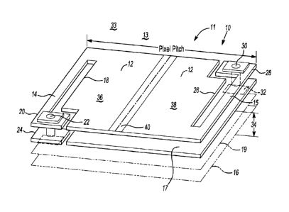
Figure 1 depicts a thermal detector (or sensor) 10 in accordance to one
embodiment of the present invention. The detector 10 may be one of many
arranged in an M x N
array 18 within a camera 11 that includes a lens 13. The camera 11 is
generally configured to
capture an image of a scene. Each detector 10 is configured to absorb IR
radiation from a scene
and to change its voltage potential based on the amount of energy received
from the scene. A
readout integrated circuit (ROIC) 19 (or readout circuit) is positioned below
each detector 10. The
ROIC 19 may electrically output the voltage potential for each detector 10.
Each detector 10 may
be micro-machined on top of the ROIC 19. The embodiments disclosed herein may
be
incorporated in a detector as set forth in co-pending application Serial No.
PCT/US2010/028293
("the '293 application"), entitled "INFRARED DETECTOR" filed on March 23,
2010. The
detector 10 is generally arranged as a micro-bridge. The detector 10 may be
formed as a
thermopile.
While the detector 10 as noted above may be used to capture an image of a
scene
in a camera, it is further contemplated that the detector 10 may be used to
sense thermal energy
from a light source (or scene), such as thermal energy received directly or
indirectly from the sun.
The detector 10 provides a voltage output in response to the thermal energy
for providing
electrical energy to power another device or for storing electrical energy on
a storage device such
as a battery or other suitable mechanism.
The detector 10 includes an absorber 12, a first arm 14, a second arm 15, and
a
substrate 16. The absorber 12, the first arm 14, and the second arm 15 may
comprise
thermoelectric materials and be formed with superlattice quantum well
materials which will be
described in more detail below. The substrate 16 may comprise, but not limited
to, a
monocrystalline silicon wafer or a silicon wafer. The substrate 16 may be
connected to the ROIC
19. The absorber 12, the first arm 14, and the second arm 15 are generally
suspended over the
ROIC 19. The first arm 14 is positioned next to the absorber 12 and may
extend, if desired
(attached or unattached) along a first side 18 of the absorber 12 and
- 5 -
CA 2813755 2018-01-11
PCT/US11/55220 13-08-2012 CA 02813755 2013-04-04
terminate at a terminal end 20. A post 22 is coupled to the terminal end 20 of
the
first arm 14.
An input pad 24 of the ROIC 19 receives the post 22. The post 22
provides an electrical connection from the absorber 12 to the ROIC 19. In a
similar manner, the second arm 15 is positioned next to the absorber 12 and
may
extend, if desired (attached or unattached) along a second side 26 of the
absorber
12 and terminate at a terminal end 28. A post 30 is coupled to the terminal
end 28
of the second arm 15. An input pad 32 of the ROIC 19 receives the post 30. The
post 30 provides an electrical connection from the absorber 12 to the ROIC 19.
In
general, the posts 22 and 30 cooperate with one another to support the
absorber 12,
the first arm 14, and the second arm 15 above the substrate 16 (e.g., suspend
the
absorber 12, the first arm 14, and the second arm 15 above the substrate 16).
The absorber 12 is generally configured to receive (or absorb) IR
radiation from a scene and to change temperature in response thereto. The
detector
may change its voltage potential based on the amount of radiation received
from
the scene. A reflector 17 is positioned between the absorber 12 and the ROIC
19.
The reflector 17 may enhance the ability for the absorber 12 to absorb the IR
radiation. The first arm 14 and the second arm 15 may be horizontally
displaced
from the absorber 12 to thermally isolate the absorber 12. It may be desirable
to
reduce thermal conduction to increase detector 10 performance. In addition,
the
absorber 12, first arm 14, and the second arm 15 may be vertically displaced
from
the substrate 16 and define an isolation gap 34 (or cavity) therebetween for
thermally isolating one detector from additional detectors positioned within
the
array.
The detector 10 may comprise P-type materials on one side and N-
type materials on another side. For example, the absorber 12 may be considered
to
include a first portion 36, a second portion 38, and an active region 40. The
first
arm 14 and the first portion 36 may be constructed from P-type materials. The
second arm 15 and the second portion 38 may be constructed from N-type
materials. The active region 40 electrically couples the P-type based elements
(first arm 14 and the first portion 36) to the N-type based elements (second
arm 15
and the second portion 38).
- 6
AMENDED SHEET - IPEA/US
CA 02813755 2013-04-04
WO 2012/051060
PCT/US2011/055220
Figure 2 depicts a thermal detector 10' in accordance to another
embodiment of the present invention. The detector 10' may be one of many
arranged in an M x N array 18 within the camera 11 that includes a lens 13.
The
detector 10' is generally similar to the detector 10 of Figure 1, but is
surface-micro-
machined.
The detector 10' is configured to absorb IR radiation from a scene
and to change a voltage potential thereof based on amount of energy received
from
the scene. An electrical connection 21 is formed on each side of the detector
10'
for providing an electrical output therefrom to a readout circuit (not shown).
The
detector 10' may also be incorporated as a detector as set forth in the '293
application.
The detector 10' includes the absorber, first arm 14, the second arm
15 and the substrate 16. The absorber 12, the first arm 14 and the second arm
15
may comprise thermoelectric materials and are formed with superlattice quantum
well materials which will also be described in more detail below. The
substrate 16
may comprise, but not limited to, a monocrystalline silicon wafer or silicon
wafer.
The absorber 12, the first arm 14 and the second arm 15 are generally
positioned
(or suspended) over a cavity 25 (see Figure 3). In a similar manner to that
described above, the first arm 14 may extend, if desired (attached or
unattached),
along the first side 18 of the absorber 12 and reach the electrical connection
21.
The second arm 16 may extend, if desired (attached or unattached), along the
second side 26 of the absorber 12 and reach the electrical connection 21.
Figure 3 depicts a thermal detector 10" in accordance to another
embodiment of the present invention. The detector 10" generally includes the
absorber 12 and may be positioned as a single detector for a thermal sensing
application. The detector 10" may be bulk micro-machined. In this
configuration,
arms are not present. The absorber 12 may comprise thermoelectric materials
and
be formed with sup erlattice quantum well materials. The electrical connection
21
is formed on each side of the absorber 12 for providing an electrical output
from
the detector 10". The absorber 12 is generally suspended over the cavity 25.
The
-7-
CA 02813755 2013-04-04
WO 2012/051060
PCT/US2011/055220
detectors (10, 10' and/or 10") as previously to referred to, will hereafter be
designated as "10."
It is known to implement an IR detector that includes arms and an
absorber being suspended over the substrate. In this conventional approach,
the
arms thermally isolate the absorber, which in turn causes a reduction in
thermal
conductance from the absorber to the substrate. By reducing thermal
conductance
between the absorber 12 and the arms 14, 15, heat transfer/leakage may be
reduced
and an improvement in IR detector performance may be realized. This
conventional approach generally forms the thermoelectric structure (e.g., the
arms
and the absorber) with one or more of the following materials: bismuth-
telluride,
antimony-telluride, lead telluride, polysilicon, polysilicon-germanium,
skutterudite, a nano-composite material, and a superlattice structure in order
to
achieve low thermal conductivity. By forming the detector with one or more of
the
aforementioned materials and by suspending the absorber and the arms, these
conditions may cause the absorber and/or the arms to warp or buckle which may
lead to a detector failure.
The embodiments described herein recognize, inter alia, that the
absorber 12 and/or the arms 14, 15 as used in connection with an IR sensing
device
may be constructed with superlattice quantum well thermoelectric materials
that
may enable the detector 10 to realize adequate detector performance
characteristics. Moreover, the embodiments disclosed herein contemplate
encapsulating the superlattice quantum well materials of the absorber 12
and/or the
arms 14, 15 with silicon nitride or silicon dioxide. The encapsulation of the
absorber 12 and/or the arms 14, 15 with the silicon based materials may
compensate or equalize stress that is induced during the deposition of the
superlattice quantum well materials and increase the mechanical strength of
the
detector 10 while portions of the detector 10 are suspended over the ROTC 16.
By
increasing the mechanical strength of the detector 10 and by stress
compensating
the detector 10, warping or buckling of the detector 10 may be minimized or
eliminated altogether. The embodiments further recognize that the absorber 12,
the
first arm 14, and the second arm 15 of the detector 10 may be constructed from
superlattice (e.g., silicon/-silicon-germanium (Si/SixGehx) where x may be an
integer or a non-integer (hereafter "Si/SiGe")) quantum well thermoelectric
-8-
CA 02813755 2013-04-04
WO 2012/051060
PCT/US2011/055220
materials. The first arm 14 and the first portion 36 may be formed of a P type
superlattice quantum well thermoelectric material. The second arm 15 and the
second portion 38 may be formed of an N type superlattice quantum well
material.
By utilizing a superlattice quantum well thermopile 10 that includes
the absorber 12 and/or arms 14, 15, such a condition minimizes thermal loss
from
the absorber 12 through the arms 14, 15 to substrate 16 and/or to any devices
positioned proximate to the absorber 12, thereby thermally isolating the
absorber
12 from a surrounding device. When IR from a scene heats the absorber 12, the
detector 10 generates an output voltage that is proportional to the
temperature
difference between the absorber 12 and the substrate 16. Accordingly, if the
absorber 12 was formed of material containing a high thermal conduction,
detector
performance may be adversely affected due to the leakage of thermal energy
from
the absorber 12. Because the superlattice quantum well material provides a low
thermal conductivity, adequate thermal isolation at the absorber 12 may be
achieved, thereby improving detector performance. In addition, superlattice
quantum well materials also provide for a high Seebeck coefficient and high
electrical conductivity which enables the detector 10 to provide an output
voltage
with a high signal-to-noise ratio which provides for a high fidelity
representation
of the amount of IR radiation sensed by absorber 12. Generally, the detector
10
may not provide for current flow. However, in some embodiments the detector 10
is capable of providing a flow of current in the milliamp range.
While conventional IR detectors are known to include bismuth-
telluride, antimony-telluride, lead telluride, polysilicon, polysilicon-
germanium,
skutterudite, a nano-composite material, and a superlattice structure as a
means to
achieve low thermal conductivity (i.e., minimize heat dissipation or transfer
from
the detector) for a suspended absorber and/or suspended arms, such materials
may
not provide sufficient mechanical support or not be properly stress
compensated. It
can be seen (as shown below) that the use of superlattice quantum well
thermoelectric materials in the detector 10 may provide for adequate thermal
conductivity and may serve as an alternate to the types of materials in
conventional
detectors.
-9-
CA 02813755 2013-04-04
WO 2012/051060 PCT/US2011/055220
In general, in order to obtain a large response from a thermopile
detector 10, the thermal conductance from the detector 10 (e.g., absorber 12
and/or
the arms 14, 15) to the thermal ground plane (e.g., within the substrate 16),
Gic,
should be small. Therefore, the thermal conductivity of the thermopile
material
should be as small as possible. Conclusively, it may be desirable for the
material
within the detector 10 to have (a) a high Seebeck coefficient and (b) a high
electrical conductivity. A figure of merit for a thermopile made of n-type and
p-type materials is defined as follows:
2
ap aõ
Z - _______________________________________
[frpk) p,112
+ (1-,1c,)112] 2
1 0 (I)
Where:
= Seebeck constant for p-type material in Volts
an= Seebeck constant for n-type material in Volts
Watt
kp= Thermal conductivity for p-type material in
m=K
Icn= Thermal conductivity for n-type material ¨Watt
tn=K
p= Resistivity of p-type material in f2=In
pyi= Resistivity of n-type material in .in
This figure of merit may not be representative of Signal to Noise
Ratio related to thermal imaging because it may not be proportional to the
common
figure of merit for IR detectors, detectivity or D*. A more appropriate figure
of
merit may be one that is proportional to D*:
(a, ¨an)
Z
D* = R + pp )1I2(kp +k,)]
(2)
This new figure of merit assumes that the arms 14, 15 have the
same length and cross-sectional area. Table 1 (below) shows this new figure of
merit for a selected group of materials. Performance improvement based on
thermopile material choice may be evident.
-10-
CA 02813755 2013-04-04
WO 2012/051060 PCT/US2011/055220
Thermopile Material Type
polysilicon Si0.7Ge0.3 Bi2Te3/Sb2 QW
polysilicon Te Si/SiGe
3
post- NO YES YES YES
CMOS
Compatible
Z FoM 1.9x10⁻² 8.1x10² 2.8x10⁻¹ 1.6
(w/cm)-1/2
Table 1: FPA Thermocouple Materials
For small pitch (e.g., 50i..un) arrays, Bi2Te3 and np Si0.7Ge0.3 may
be practical choices for the thermoelectric materials. The reason for
rejecting
standard np polysilicon is that its thermal conductivity may be too large to
achieve
reasonable detector sensitivities. Moreover, the deposition temperature may be
too
high for post Complementary Metal-Oxide-Semiconductor (CMOS) compatibility.
The measurements of interest (e.g., resistivity, Seebeck coefficient, and
thermal
conductivity) for quantum well Si/SiGe, Bi2Te3, Si0.7Ge0.3 and standard np
polysilicon are given below in the Table 2:
Thermopile Resistivity ?Alin
b .Z
k m
Material Type See eck
QW Si/SiGe 0.1 to 10.0 12001 3-5
(NP)
Bi2Te3 (N) 12.6 -248 1.3
Sb2Te3 (P) 12.6 188 1.8
Bi2 Te3 -Bi2 Se,(N) 15 -200 1.2
.1
Bi2Te-Sb2Te3(P) 12 240 1.2
Si0.7 Ge0.3 10 to 1000 100 to 15001 5
polysilicon (NP)
polysilicon (NP) 10 to 1000 1001to 15001 23
Table 2: Bi2Te3/Sb2Te3 Parameters, Polysilicon Parameters, QW Parameters
Although Bi2Te3 and Sb2Te3 can produce high performing
thermopile detectors, choosing Bi2Te3 and Sb2Te3 may have several drawbacks.
-11-
CA 02813755 2013-04-04
WO 2012/051060
PCT/US2011/055220
For example, (1) detector resistance can fall around 3k1/ and a consequence is
that
electronic noise may dominate; (2) deposition and etching of Bi2Te3 and Sb2Te3
is
being heavily researched and may not be mature yet (however, Bi2Te3 and Sb2Te3
can be deposited at low temperatures, patterned and dry etched); (3) the
Temperature Coefficient of Responsivity (TC93) (z0.1%) may be higher than np
Si0.7 Ge0.3 (<0.04%) (e.g., a lower TC93. may require less effort in
temperature
compensation of the responsivity); and (4) the thermoelectric properties of
Bi2Te3
and Sb2Te3 may vary greatly if the stoichiometry is not maintained which
implies
tight controls on the deposition and non-conventional deposition processes
such as
co-evaporation. In contrast, Si/SiGe superlattice quantum wells comprise
widely
used materials in CMOS and Micromechanical Systems (MEMS) processing.
Moreover, stoichiometry may not be an issue in the Si/SiGe superlattice
quantum
well implementation, which may allow deposition to be conducted with less
critical, controls.
The thermal conductivity of Bi2Te3 thin films has been measured to
be 1.2 ¨mK which may be close the thermal conductivity of PECVD silicon
nitride,
where thermal conductivity may be -1.18 ¨mK. The thermal conductivity of bulk
Bi2Te3 may be 1.7 ¨mK and the lower thermal conductivity may be a common
effect
in very thin films. The thermal conductivity of Bi2Te3 may fall further as the
film
thickness falls below 0.5um.
As shown above in Table 2, Bi2 Te, and silicon nitride may have
.1
similar thermal conductivities. Due to this fact, adding significant amounts
of
silicon nitride to the arms and/or to the absorber when formed of Bi2Te3 may
cause
a decrease in detector performance. Due to this condition, conventional
implementations tend to avoid adding silicon nitride or silicon dioxide to
bismuth
telluride based detectors. In contrast, the arms 14, 15 and/or the absorber 12
of the
present disclosure may include various amounts of silicon nitride and/or
silicon
dioxide with quantum well Si/SiGe. This condition may not cause a significant
loss in detector performance because the thermal conductivity of quantum well
Si/SiGe may be 3-4 times greater than that of silicon nitride. As such, the
addition of the thermal conductivity added by the silicon nitride may be
negligible
-12-
CA 02813755 2013-04-04
WO 2012/051060
PCT/US2011/055220
in terms of the overall increase in thermal conductivity added to the Si/SiGe
quantum well with the silicon nitride. For example, the thermal conductivity
of
Si/SiGe quantum well may be between 3 ¨ 5 W,/mK. The thermal conductivity of
the silicon nitride may be 1.2 W/mK. Adding moderate amounts of the silicon
nitride may not affect detector performance because the thermal conductivity
of the
Si/SiGe quantum well may dominate. In general, the thickness of the silicon
nitride may be anywhere from 10% to 100% of the overall thickness of the
quantum well arms 14, 15. For example, if the arms 14, 15 are 1000A thick,
then
the thickness of the silicon nitride may be in the range of 100A to 1000A. In
general, the largest component of the total thermal conductance is due to the
arms
14, 15.
Conventional based detectors that may implement a suspended arm
and absorber structure tend to avoid encapsulating the arms and/or the
absorber
with silicon nitride when bismuth telluride materials are used to form the
films in
the detector to prevent an increase in thermal conductivity. However, it has
been
discovered as set forth herein, that by removing the encapsulated silicon
nitride,
such a condition may aid to the warping and/or buckling of the detector 10 as
noted
above. For example, the removal of the encapsulated silicon nitride may
decrease
detector mechanical strength and remove the capability to stress compensate.
Unless the detector is stress compensated, the detector may warp and become
non-
functional.
Another useful dielectric in MEMS processing may be silicon
dioxide. When deposited, silicon dioxide may normally be in compressive
stress,
this material in conjunction with silicon nitride can be used to compensate
for
stress and additionally may be an effective etch stop. The thermal
conductivity of
W
thin film silicon dioxide may be 2.0m¨K.
Figure 5 depicts a superlattice quantum well thermoelectric material
that is encapsulated by silicon materials. In general, the sup erl atti ce
quantum well
layers of the absorber 12, and/or the arms 14, 15 and may be sandwiched
between
a top layer of silicon nitride and a bottom layer of silicon nitride (or
sandwiched
between a top layer of silicon dioxide and a bottom layer of silicon dioxide
or
sandwiched between a top layer of silicon nitride and a bottom layer of
silicon
-13-
CA 02813755 2013-04-04
WO 2012/051060
PCT/US2011/055220
dioxide (or vice versa) (see, element 29 in Figure 2 alternating layers of
Si/SiGe
(e.g., barrier or conducting layers where the barrier layers comprise Si and
the
conducting layers comprise SiGe)). In reference to Figures 1-2, the first arm
14
and the first portion 36 may be formed a p-type superlattice quantum well that
is
encapsulated by silicon nitride. Conversely, the second arm 15 and the second
portion 38 may formed of an n-type superlattice quantum well that is
encapsulated
by silicon nitride. The SiGe layer positioned above the silicon nitride layer
may
include a high Ge content polysilicon SiGe seed layer. The Ge content may be
at
least 70 %. When deposited at low temperatures, the high Ge of SiGe seed layer
may form polysilicon-germanium which may have a somewhat ordered crystalline
structure on which to lay down the next layer of silicon.
Figures 6A ¨ 6B depict one embodiment that realizes a quantum
well effect and another embodiment that does not realize a quantum well
effect,
respectively. In reference to Figure 3a, a portion of the detector (e.g.,
first arm 14,
second arm 15, and/or absorber 16) may include any number of films 41. The
films 41 may comprise alternating layers of Si and Si/Ge (e.g., superlattice
of Si
and Si/Ge). Each layer of Si and Si/Ge may have a thickness of 200A. The total
thickness of the quantum well material within the detector 10 may be < 2000A.
A
first contact 42 is positioned on one end and a second contact 44 is
positioned on
another end. The first contact 42 may be horizontally positioned away from the
second contact 44. By positioning the first contact 42 horizontally away from
the
second contact 44, small amounts of current and heat may flow laterally, from
the
first contact 42 through the layers of Si/SiGe to the second contact 44 (e.g.,
in
plane). Such a condition enables the first arm 14, the second arm, and/or the
absorber 16 to realize the quantum well effect.
One approach to increasing the performance of thermoelectric
materials may be to form compositionally modulated materials, mainly by
quantum well confinement of carriers in the active layers in a multilayer film
by
adjacent barrier layers. The approach as disclosed herein is to enclose each
electrically active layer by a material which has a band offset sufficient to
form a
barrier for the charge carriers. An improvement in the thermoelectric
properties
(e.g., Seebeck effect, electrical resistivity and thermal conductivity) is
expected to
follow from an increase in the density of states (e.g., increased Seebeck), an
-14-
CA 02813755 2013-04-04
WO 2012/051060
PCT/US2011/055220
increase in carrier mobility (e.g., lower electrical resistance), and
inhibited phonon
flow due to strain between the quantum well and barrier layers (e.g., lower
thermal
conductivity). The layer thicknesses may be < 200A.
Figure 6B depicts that the first contact 42 is vertically displaced
from the second contact 44. Small amounts of current and heat may flow in a
cross-plane direction which is perpendicular to the in-plane direction of the
quantum well configuration noted above from the first contact 42 through the
layers of Si/SiGe to the second contact 44. While thermal conductivity may be
reduced, this implementation fails to realize the quantum well effect.
Figure 7 depicts the various stresses caused by the layers of silicon
nitride and the superlattice quantum well materials during deposition in one
or
more of the absorber 12 and/or in the arms 14, 15. For example, materials such
as
quantum well Si/SiGe when deposited, could be in a state of compressive
stress.
Under compressive stress, the various layers of Si and SiGe may expand with
respect to the substrate 16. In this state of stress, the layers of Si and
Si/Ge (either
in the absorber 12 and/or in the arms 14, 15) when suspended and attached at
two
points (e.g., at the posts 22, 30), may buckle over the substrate 16.
The silicon nitride on the other hand, when deposited, could be in a
state of tensile strength. Under tensile stress, each layer of silicon nitride
may
shrink with respect to the substrate 16. In this state of stress, each layer
of silicon
nitride when suspended and attached at two points (e.g., at the posts 22, 30),
may
be stretched by the substrate 16. By using predetermined thickness and
deposition
parameters for the silicon nitride and the quantum well Si/SiGe, a nearly
stress free
detector may be constructed. In general, due to the fact that the two stresses
(e.g.,
compressive and tensile) are of opposite type, a nearly stress free thin film
could be
formed by combining the Si and Si/Ge layers to the silicon nitride layers. The
thickness for each layer may depend on the magnitude of the stress in each
layer.
In general, if the layers (e.g., layers of Si and Si/Ge and silicon
nitride) of the detector 10 have equal and opposite stress levels, then the
deposition
of the layers on top of one another may produce a nearly stress free film. For
example, let am, represent the stress of material, mi (e.g., the layers of Si
and
-15-
CA 02813755 2013-04-04
WO 2012/051060
PCT/US2011/055220
Si/Ge) and am, represent the stress of material, m2 (e.g., the layers of
silicon
nitride). A material that is in tensile stress may have a positive value and a
material in compressive stress may have a negative value. Let ti represent the
thickness for a first set of layers (e.g., Si and Si/Ge) and t2 represent the
thickness
for a second set of layers (e.g., silicon nitride). In order to produce a
stress
compensated detector 10, the following equation may need to be satisfied:
o-mi + o-m2t2 = 0 (3)
This expression may be easily generalized to more than two sets of
layers.
As noted above, the quantum well Si/SiGe may be in a state of
compressive stress when deposited and the silicon nitride may be in a state of
tensile stress when deposited, the compressive stress caused by the deposition
of
the quantum well Si/SiGe may be offset by the tensile stress caused by the
deposition of the silicon nitride which may result in a nearly stress free
suspended
detector implementation.
In general, each layer of SiGe may be n or p-type doped in the
absorber 12 and/or in the arms 14, 15. The Si layers may not be doped and are
therefore not electrically conductive. The doping concentration of one or more
layers of the silicon germanium in the absorber 12 and/or in the arms 14, 15
is
roughly between 5x10^18 to 5x10^19 atoms/cm^3. The doping concentration may
not be the same for the n-type and p-type. The electrical resistance of the n-
type
arm and p-type arm should be the same to maximize the Seebeck effect this is
why
the doping concentration of the various layers of silicon germanium is
different as
it may be adjusted to achieve equivalent arm resistance. Moreover, as the
doping
concentration moves up, the electrical resistance goes down, but the Seebeck
effect
also goes down. The optimal doping concentration for the layer of silicon
germanium is achieved to ensure that the electrical resistance is the same
between
the n-type and p-type arm and, moreover, to achieve maximum signal to noise
ratio.
-16-
CA 02813755 2013-04-04
WO 2012/051060
PCT/US2011/055220
The use of the superlattice quantum well based thermoelectric
materials in the detector 10 provide for, but not limited to, adequate thermal
conductivity, increased Seebeck effect, and low resistivity which may increase
detector performance. Encapsulating the superlattice quantum well based
materials with silicon based materials (such as silicon nitride and/or silicon
oxide
or other suitable materials) may increase mechanical strength of the detector
10
and stress compensate offsetting stress caused by the various layers of the
superlattice quantum well materials. In short, the present disclosure
contemplates
that the use of superlattice quantum well thermoelectric materials when
combined
with silicon based materials in the detector 10 may provide (i) increased
detector
performance due to the acceptable levels of thermal conductivity, increased
Seebeck effect and low resistivity that have been discovered to be found in
connection with the superlattice quantum well thermoelectric materials and
(ii)
increased mechanical strength/stress compensation caused by offsetting stress
between the superlattice quantum well thermoelectric materials and the
encapsulated silicon based materials.
Figure 8 depicts a fabrication process flow 50 for producing the
quantum well thermoelectric detector 10 in accordance to one embodiment of the
present invention. It is contemplated that the process flow 50 may be utilized
to
produce the detector 10. The process flow 50 depicts the fabrication of the
detector 10 without the use of silicon nitride as an etch stop.
In operation 51, form a silicon dioxide layer.
In operation 52, pattern and dry etch the silicon dioxide.
In operation 54, a layer of titanium is deposited over the layer of
silicon dioxide. Titanium, TiW, Cr, or other similar metals may be used as a
buffer
layer as aluminum may stick to these refractory metals and the refractory
metals
may stick to whatever they are deposited on.
In operation 56, a layer of aluminum is deposited over the layer of
titanium (see Figure 6A). Aluminum may provide for better electrical
conductivity
.. than refractory metals.
-17-
CA 02813755 2013-04-04
WO 2012/051060 PCT/US2011/055220
In operation 58, the aluminum and titanium (or TiW or Cr) are
patterned to form the reflector 17 and interconnects (such as the input pads
24 and
32 on the ROIC 16) (see Figure 6B).
In operation 60, a layer of polyimide is deposited over the
aluminum. Polyimide is an organic material that may be used as a sacrificial
layer.
That is in the end the polyimide may be etched away in an oxygen plasma etch.
The polyimide may be able to withstand the high temperature processing and may
be easily etched away. The polyimide may be necessary due to its ability to be
easily etched away since it may be at a bottom of the MEMS stack.
In operation 62, a portion of the polyimide is removed to define an
opening to form the posts 22, 30 later in the process 50.
In operation 64, a first layer of silicon nitride is deposited on top of
the polyimide (see Figure 9C). As noted above, when the silicon nitride is
deposited, the layer of silicon nitride may exhibit a form of tensile stress.
In operation 66, a seed layer is deposited over the ROTC 19. This
deposition may include a post-CMOS compatible SiGe polysilicon or a post-
CMOS compatible Ge. The seed layer may enable the detector 10 to achieve
sufficient quantum well performance. The seed layer may exhibit a crystalline
structure or short range ordering of its structure. For example, the Si/SiGe
layers
should at least have some sort of short range crystalline order. The reason
for this
is that the electrical conductivity may be poor because non-crystalline
materials are
known to be poor electrical conductors. It may be difficult obtaining true
poly-
silicon deposition at low temperatures (e.g., < 450 C) for Si and high Si
content
(Si,Gei,)(x > 0.4). On the other hand, high Ge content SiGe can be deposited
at
lower temperatures (e.g., < 450 C) and be polycrystalline. For example, when
the
Ge content of SixGel, is 70% (x = 0.3), good quality polysilicon Si0,3Ge0,7
can be
deposited at temperatures < 400 C. This may make a very good seed layer such
that when Si or SiGe (typically Si0,8Ge0,7) is deposited via sputtering at 350
C
the material "follows" the crystalline ordering of the lower layer thus
obtaining a
more crystalline orientation of the sputtered material. This part may be of
-18-
CA 02813755 2013-04-04
WO 2012/051060 PCT/US2011/055220
significance in producing high performance detectors. The addition of the seed
layer may enable latter deposited alternating layers of Si and SiGe to achieve
favorable quantum well thermoelectric properties. The layer of silicon dioxide
is
formed on top of the seed layer to form the substrate 16.
Alternating layers of Si and SiGe quantum well layers are also deposited to
top of the layer of silicon nitride. Each layer of Si and SiGe may be
approximately
100A. These layers of Si and SiGe may exhibit a state of compressive stress.
The
alternating layers of Si and SiGe may be n-type doped (see Figure 9C). It is
recognized that the layer of Si and SiGe may be p-type doped as well. In
general,
four to five periods of Si and SiGe may be used in the detector 10 (or 8 to 10
layers
of Si and SiGe). The thickness of the silicon nitride may be up to 1000A (if
10
layers are used). The total thickness of the silicon nitride and the
alternating layers
of Si and SiGe (assuming 10 layers of Si and SiGe (e.g., 1000 A) and an upper
limit thickness of silicon nitride (e.g., 1000 A)) has a total thickness of
2000 A.
In operation 68, a first portion 36 or 38 of the absorber 12 and the
arm 14 or 15 may be formed by way of being patterned and dry etched. This
portion of the absorber 12 and the arm 14 or 15 may be n-type.
In operation 70, photoresist is removed and a second set of
alternating layers of Si and p-type Si/Ge are deposited directly over the
layers of Si
and n-type SiGe and silicon nitride layer. In general, the photoresist define
which
areas may be etched and which areas may not be etched.
In operation 72, a second portion 36 or 38 of the absorber 12 and
the arm 14 or 15 (e.g., opposite to that formed in operation 68) may be formed
by
way of being patterned and dry etched.
In operation 74, a second layer of silicon nitride is deposited on top
of both the alternating p-type quantum well Si/Si Ge layers and the
alternating n-
type quantum well Si/SiGe layers. As noted above, when the silicon nitride is
deposited, the layer of silicon nitride may exhibit a form of tensile stress.
Both
layers of the silicon nitride provide tensile strength which may compensate
for the
-19-
CA 02813755 2013-04-04
WO 2012/051060
PCT/US2011/055220
compressive stress added to the detector 10 with the alternating quantum well
Si/SiGe layers.
In operation 76, a thin metal film is deposited over the second layer
of silicon nitride to enhance radiation absorption.
In operation 78, a portion of the second layer of silicon nitride and
the alternating layers of Si and SiGe (e.g., n-type or p-type) are removed
down to
the polyimide.
In operation 80, the portions of the thin metal film, the first and
second layers of silicon nitride, the alternating layers of Si and Si/Ge are
removed
to define an opening for forming the posts 22, 30, respectively.
In operation 82, titanium and aluminum arc deposited in the
openings formed within the arms 14, 15. The titanium and the aluminum are
deposited within the openings to form the posts 22, 30. Only titanium is
deposited
over the absorber region (see Figure 9D). This section of the detector 10 is
also
known as the active region 40 on the absorber 12.
In operation 84, the entire polyimide layer is removed with an
oxygen plasma dry etch. By removing the entire polyimide layer, the first and
second layers of the silicon nitride and the alternating layers of Si and SiGe
are
suspended over the substrate 16. The suspended layers of silicon nitride and
Si
.. and SiGe are coupled to the ROIC 19 via the posts 22, 30.
Figures 9A ¨ 9D depict various formations of the detector 10 when
being fabricated as noted in connection with Figure 8.
Fig. 10 depicts a fabrication process flow 100 for producing the
quantum well thermoelectric detector 10 in accordance to one embodiment of the
present invention. The process flow 100 depicts the fabrication of the
detector 10
with the use of silicon nitride as an etch stop.
-20-
CA 02813755 2013-04-04
WO 2012/051060
PCT/US2011/055220
Operations 101, 102, 104, 106, 108, 110, 112, 114, and 116 are
similar to operations 51, 52, 54, 56, 58, 60, 62, 64, 66, respectively, as
noted in
connection with Figure 8.
In operation 118, a second layer of silicon nitride is deposited on
top of the alternating layer n-type quantum well Si/SiGe. It is recognized
that
either p-type or n-type quantum well Si/SiGe may be deposited. As noted above,
when the silicon nitride is deposited, the layer of silicon nitride may
exhibit a form
of tensile stress. Both layers of the silicon nitride provide tensile
strength, which
may compensate for the compressive stress added to the detector 10 with the
alternating layers of the n-type quantum well Si/SiGe. The second layer of
silicon
nitride acts as a dry etch stop to protect the layers of material that are
below the
silicon nitride when additional layers of material are added later in the
fabrication
process.
In operation 120, the second layer of silicon nitride and the
alternating layers of the n-type quantum well Si/SiGe layers are dry etched to
form
the arm 15 and the second portion 38 of the absorber 12 (see Figure 11B). For
example, the second portion 38 of the absorber 12 and the arm 15 may be formed
by dry etching. This portion of the absorber 12 and the arm 15 may be n type.
In
this operation, the layers of Si/SiGe may be encapsulated by the first and
second
layers of the silicon nitride. This condition may stress compensate the arm 15
and
the second portion 38 within the detector 10.
In operation 122, photoresist is removed and a second set of
alternating layers of p-type quantum well Si/SiGe materials are deposited. The
second set of alternating layers of p-type Si/SiGe materials are deposited
directly
over the first and second layers of silicon nitride (see Figure 11C).
In operation 124, a third layer of silicon nitride is deposited on top
of the second set of alternating layers of p-type Si/SiGe materials (see
Figure 11C).
In operation 126, the third layer of silicon nitride and the second set
of alternating layers of Si and p-type Si/SiGe are dry etched to form the
first arm
14 and the first portion 36 of the absorber 12. In this operation, the first
of second
-21-
CA 02813755 2013-04-04
WO 2012/051060 PCT/US2011/055220
alternating layers of Si and p-type Si/SiGe materials may be encapsulated by
the
first and third layers of the silicon nitride (see Figure 9D). This condition
may
stress compensate the arms 14, 15 and the first and second portion 36, 38
within
the detector 10.
In operation 128, a thin metal film is deposited over the second
layer of silicon nitride and the third layer of silicon nitride on the
absorber 12. The
thin metal film is configured to enhance IR absorption (see Figure 11E).
In operation 130, a portion of the second and third layers of silicon
nitride and the alternating layers of Si and SiGe (e.g., n-type or p-type) are
removed down to the polyimide to form the thermopile arms.
In operation 132, the portions of the thin metal film, the first,
second, and third layers of silicon nitride, and the alternating layers of Si
and Si/Ge
are removed on the arms 14, 15 to define an opening for forming the posts 22,
30.
In operation 134, titanium and aluminum are deposited in the
openings formed within the arms 14, 15. The titanium and the aluminum are
deposited within the openings to form the posts 22, 30. Only titanium is
deposited
over the absorber region. This section of the detector 10 is also known as the
active region 40 on the absorber 12.
In operation 136, the entire polyimide layer is removed with an
oxygen plasma dry etch. By removing the entire polyimide layer, the first and
second layers of the silicon nitride and the alternating layers of Si and SiGe
are
suspended over the substrate 16. The suspended layers of silicon nitride and
Si
and SiGe are coupled to the ROIC 19 via the posts 22, 30.
While embodiments of the invention have been illustrated and
described, it is not intended that these embodiments illustrate and describe
all
possible forms of the invention. Rather, the words used in the specification
are
words of description rather than limitation, and it is understood that various
changes may be made without departing from the spirit and scope of the
invention.
-22-