Note: Descriptions are shown in the official language in which they were submitted.
CA 02887694 2015-04-14
WO 2014/090356 PCT/EP2013/003276
1
Contact element and method for its manufacture
The invention relates to a contact element having contact points for the
electrically conductive connection of contact regions of mutually spaced
elements, for example circuit boards. The invention also relates to a
method for the manufacture of such a contact element as well as a
contact device which comprises a plurality of such contact elements.
Contact elements of the generic type are for example used to form so-
called board-to-board (B2B) connectors, by means of which two circuit
boards arranged at a distance from one another are connected in an
electrically conductive manner.
The contact elements should thereby ensure an as far as possible loss-
free transmission of the radio frequency signals, including within a defined
tolerance range in terms of parallel alignment and spacing as well as any
lateral offset of the two circuit boards or their contact regions. Further
requirements are economical manufacture and simple assembly. In
addition, the axial and radial dimensions of the contact elements should
be as small as possible, since the continuing further miniaturisation of
circuit boards and the circuit traces applied to them means that the
CA 02887694 2015-04-14
WO 2014/090356 PCT/EP2013/003276
2
number of contact elements which need to be arranged next to one
another within a limited space. is increasing all the time.
It is known for a connection between two circuit boards to be established
by means of two coaxial plug connectors permanently connected with the
circuit boards together with an adapter connecting the two coaxial plug
connectors, the so-called "bullet". This adapter makes possible a
compensation of axial and radial tolerances, as well as the compensation
of parallel alignment tolerances. Typical coaxial plug connectors used for
this purpose are SMP, Mini-SMP or FMC.
Alternatively, electrical connections between two circuit boards are also
realised by means of spring-loaded contact pins in individual conductor
and/or multiple conductor design. Such spring-loaded contact pins
comprise a sleeve and head which is partially guided within the sleeve as
well as a helical spring which is supported between the head and the
sleeve. The properties required of the helical spring in terms of spring
force and block length demand relatively long spring lengths, which have
a correspondingly disadvantageous effect on the axial construction height
of the spring-loaded contact pins.
A coaxial contact element is also known from US 6,776,668 B1 by means
of which radio frequency signals are to be transferred between two circuit
boards. An inner conductor, which is designed in the form of a spring-
loaded contact pin, serves as a signal conductor, while an outer conductor
surrounding the inner conductor performs the function of a return
conductor as well as acting as a shield for the inner conductor. The outer
conductor comprises a sleeve-formed base body which is split several
times in the longitudinal direction. The unsplit end of the base body forms
on its end face a contact point for making contact with a contact region of
one of the circuit boards. A sleeve of the outer conductor is guided
displaceably on the base body and forms on one end face a contact point
WO 201410903$6
PCT/EP2013/003276
3
for making contact with a contact region of the other circuit board. A pre-
tensioned spring is supported between the base body and the sleeve.
When the two circuit boards are connected, both the head of the Inner
conductor and the sleeve of the outer conductor are displaced, with
further tensioning of the relevant springs, as a result of which a more
reliable contact pressure can be provided, despite possible tolerances in
terms of the distance between the contact regions of the circuit boards. In
addition, the splitting of the base body means that this also possesses a
certain flexibility in a lateral direction, which is intended to ensure that
even relatively large deviations in parallel alignment between the two
contact regions can be compensated.
Fundamentally, the known contact elements have relatively large
dimensions, which, moreover, as a result of their construction design and
the resulting function, cannot be reduced indefinitely. For example, a
reduction in the diameter of plug-socket connections such as are used,
inter alia, in the aforementioned SMP plug connectors, is only possible up
to a certain limit, since otherwise with the materials usually used problems
would arise with regard to the strength of plug and socket, in particular
when plugging together the plug connection.
Starting out from this state of the art, the invention was based on the
problem of providing a contact element of the generic type which is
distinguished through extremely small dimensions, making it possible to
create a contact device in which the greatest possible number of such
contact elements are accommodated within a predetermined space.
CA 2887694 2018-09-18
WO 2014/090356
PCT/E132013/003276
4
The basic concept behind the invention is to achieve a miniaturisation of a
contact element of the generic type through the use of alternative
manufacturing methods not previously used for the manufacture of such
contact elements. This basic concept was also based on the knowledge
that a simple miniaturisation of the known contact elements cannot lead to
success, among other things due to the strength problems already
mentioned; rather, such miniaturisation must at the same time be
combined with a change in the functional design. A further realisation was
that such a functional redesign in combination with the desired
dimensions can probably only be achieved if the contact element is
formed as a single part. The alternative manufacturing method which was
sought thus had to make it possible to create highly-complex geometries
in extremely small dimensions at reasonable cost, whereby it had to be
possible to process a material which allows the integration of the
functionalities required of contact elements of the generic type.
This basic concept behind the invention is implemented in a (three-
dimensional) contact element with contact points for the electrically
conductive connection, bridging a space, of contact regions of mutually
spaced elements, in particular circuit boards, which is formed completely
of one or more deposited materials, of which at least one is electrically
conductive.
The deposition of materials makes it possible to form extremely small yet
highly complex geometries. Due to the electrically conductive properties
and good elasticity of many metals, the preferred use of a metal for
deposition and thus for the formation of the contact elements, which is
also proposed, makes it possible to integrate in the miniaturised contact
CA 2887694 2018-09-18
CA 02887694 2015-04-14
WO 2014/090356 PCT/EP2013/003276
element the important functionalities required of contact elements of the
generic type, namely electrical conductivity as well as the generation of a
contact pressure ensuring a good contact between the contact points and
the contact regions of the elements which are to be connected. Instead of
forming the contact element completely of one of more deposited metals,
plastics, for example, can also be used. For this purpose, these should
preferably display the required elasticity and/or be electrically conductive.
Alternatively however, a contact element consisting in part of plastic can
be made electrically conductive through the additional deposition of one or
more metallic layers, in particular being coated in a final deposition step.
Any suitable method known from the prior art can be used for the
deposition of the material or materials. Particularly preferred methods for
the deposition and thus for the manufacture of a contact element
according to the invention are the so-called LIGA methods. The term
"LiGA" is a German acronym for the terms describing the key steps in this
method "Lithographie, Galvanik, Abformung" (lithography, electroplating
and moulding).
The LiGA method, or methods (numerous variants are possible) is
distinguished in that it makes it possible to manufacture microstructures
with extremely small dimensions of for example 0.2 pm, structure heights
of up to 3 mm, and aspect ratios of for example 50 (for detailed structures,
up to as much as 500) from, for example, plastics, metals or ceramics.
In order to manufacture a contact element by means of a LiGA method it
can in particular be the case that a photosensitive or X-ray-sensitive resist
layer of, in particular, polymethyl methacrylate (PMMA), is applied to a flat
substrate, for example a silicon wafer or a polished plate of, for example,
beryllium, copper or titanium, which can be in the form of a negative
resist, but is preferably a positive resist. If the substrate itself is not
electrically conductive, this can be provided with a metallic seed layer.
CA 02887694 2015-04-14
WO 2014/090356 PCT/EP2013/003276
6
This can in particular be effected through "sputtering" or evaporation. The
resist layer is then exposed and developed, as a result of which a
negative form of the contact element which is to be manufactured is
produced. In a deposition process, a material, preferably metal (or also
several materials or metals, in layers) is deposited on the substrate in the
negative form. Preferably, the material or materials are deposited
galvanically, whereby other deposition processes, for example PVD or
CVD, are also possible. Following removal of the remaining resist, there
remain initially the substrate, the seed layer and the deposited material.
This can already constitute the contact element, insofar as an electrically
conductive material, in particular a metal, was deposited in at least one
layer. The contact element can then be detached from the substrate, for
example through etching of the seed layer.
Alternatively, the finally deposited structure can also be used as the mould
of a moulding tool. For this purpose, a further deposition can take place
with, in particular, an "overgrowth" (of a part of) the remaining resist layer
and subsequent removal of the substrate and seed layer. The contact
element which is to be manufactured can then be manufactured by means
of injection moulding or hot embossing, for example. This method is, in
particular, suitable for the manufacture of a contact element or of a base
body of the contact element which is made of plastic. If the plastic is not
electrically conductive, then in addition an electrically conductive material,
in particular a metal, can be deposited in the form of a coating.
If deposited structures with a greater thickness are required, the described
method can be used to create a mask, which is in turn then used for the
selective exposure of a thicker resist layer. In these cases, gold is
frequently deposited in the mask, which is distinguished through its
effective absorption of X-ray radiation. In addition, the gold can be
deposited on a titanium membrane (which was thus positioned between
CA 02887694 2015-04-14
WO 2014/090356 PCT/EP2013/003276
7
the substrate and the resist layer during the creation of the mask), which
is distinguished through an extremely low absorption of X-ray radiation.
In particular, X-rays or ultraviolet (UV) light can be used for exposure of
the resist layer, whereby the use of X-ray radiation tends to promise
higher precision and the use of UV light lower costs.
In order to achieve the most economical possible manufacture of a
contact element according to the invention by means of a method
according to the invention, a plurality of directly or indirectly connected
contact elements can preferably be created simultaneously by means of a
LiGA method and subsequently separated.
In a preferred embodiment, the contact element according to the invention
can possess (at least) one spring section which is elastically deformed
when contact is made with the contact regions. This spring section, which
is distinguished from the other section(s) of the contact element through a
lower spring stiffness in relation to the direction of connection, i.e. the
connecting line between the contact points, can in particular serve to
compensate tolerances of form and position of the contact element and
the contact regions which are to be connected as well as to ensure a
defined contact pressure.
Particularly preferably, the spring section is arranged between two rigid
supporting sections which do not deform, to any relevant or functional
extent, under the forces which regularly occur when contact is made with
the contact regions. The supporting sections can in particular ensure a
good stability (against kinking) of the contact element.
The spring section can preferably be meander-formed. Such a spring
section can readily be manufactured by means of the method according to
the invention.
CA 02887694 2015-04-14
WO 2014/090356 PCT/EP2013/003276
Alternatively, the spring section can possess several coaxially arranged
curved spring tabs. Such spring tabs can also readily be manufactured
according to the invention. Particularly preferably, it can also be the case
that that adjacent spring tabs make contact when contact is made with the
two contact regions as a result of the deformation of the spring section. As
a result, the spring section, insofar as this is part of the signal or current
path, can have a relatively low electrical resistance.
In a further preferred embodiment of the contact element according to the
invention, a snap-lock connection can be provided which holds the contact
element in a position in which the spring section is partially deformed. This
means that the spring section can already be pre-tensioned in an
unloaded neutral position of the contact element, as a result of which this
can already generate a relatively high contact pressure when contact is
made with the contact regions with only a slight further deformation taking
place.
It can also preferably be the case that that on a further deformation of the
spring section the sections forming the snap-lock connection slide against
one another. The sections forming the snap-lock connection (these can
preferably be the supporting sections) can thus guide the relative
movement of the sections connected through the spring section, thus
positively influencing the stability of the contact element.
In order to manufacture such a contact element, it can be the case that
the contact element(s) is/are only deformed in order to snap in the snap-
lock connection(s) following manufacture and possibly following
separation.
In a further preferred embodiment of the contact element according to the
invention, a signal or current path can be formed between the contact
CA 02887694 2015-04-14
WO 2014/090356 PCT/EP2013/003276
9
points which bypasses the spring section(s). This embodiment is based
on the idea that the spring section is generally characterised by relatively
small cross sections of the deposited electrically conductive materials and
thus by a relatively high electrical resistance. A signal or current path
should thus extend, without including the spring section, over the other
sections of the contact element, which preferably have larger cross-
sectional areas.
A contact device according to the invention comprises a (preferably at
least partially electrically insulating) mounting which possesses a plurality
of through-openings arranged next to one another, as well as several
contact elements according to the invention, whereby the contact
elements are arranged in the through-openings of the mounting, with the
sections containing the contact points projecting beyond the mounting. In
this way, a simple-to-handle unit with a plurality of contact elements
according to the invention can be created. In addition, the contact
elements can be supported in the through-openings, in a lateral direction,
by the mounting.
The invention is described in more detail in the following with reference to
exemplary embodiments illustrated in the drawings, in which:
Fig.1: shows a perspective
view of a first embodiment of a contact
element according to the invention;
Fig. 2: shows a side view of the contact element according to Fig. 1;
Fig. 3: shows an enlargement of the section III in Fig. 2;
Fig. 4: shows an enlargement of the section IV in Fig. 2;
Fig. 5: shows an enlargement of the section V in Fig. 2;
CA 02887694 2015-04-14
WO 2014/090356 PCT/EP2013/003276
11)
Fig. 6: shows an enlargement of the section VI in Fig. 2;
Fig. 7: shows a section of a contact device according to the invention
with contact elements according to Fig. 1 to 6 in a cross section;
Fig. 8: shows an arrangement of the contact elements in the contact
device according to Fig. 7;
Fig. 9: shows a perspective view of a second embodiment of a contact
element according to the invention;
Fig. 10: shows a section of a contact device according to the invention
with contact elements according to Fig. 10 to 12 in a cross
section;
Fig. 11: shows an arrangement of the contact elements in the contact
device according to Fig. 12;
Fig. 12: shows a perspective exploded view of a system consisting of
two circuit boards and a contact device according to Fig. 11;
Fig. 13: shows a side view of the system according to Fig. 12;
Fig. 14: shows an enlargement of the section XIV in Fig. 12;
Fig. 15: shows a side view of a third embodiment of a contact element
according to the invention;
Fig. 16: shows a plurality of jointly manufactured contact elements
according to Fig. 15;
CA 02887694 2015-04-14
WO 2014/090356 PCT/EP2013/003276
11
Fig.17: shows a fourth embodiment of a contact element according to
the invention in a first position;
Fig. 18: shows the contact element according to Fig. 17 in a second
position;
Fig. 19: shows the contact element according to Fig. 17 in a third
position;
Fig. 20: shows a perspective view of a contact device according to the
invention with contact elements according to Fig. 17 to 19;
Fig. 21: shows a diagonal section through the contact device according
to Fig. 20;
Fig. 22: shows a fifth embodiment of a contact element according to the
invention in a first position;
Fig. 23: shows a first step of a method according to the invention;
Fig. 24: shows a second step of a method according to the invention;
Fig. 25: shows a third step of a method according to the invention; and
Fig. 26: shows a fourth step of a method according to the invention.
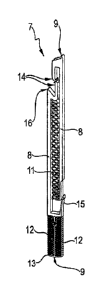
A first embodiment of a contact element 7 according to the invention is
illustrated in Figs. 1 to 6. According to the invention, the one-part contact
element 7, formed of an electrically conductive metal, has been
manufactured by means of a LiGA method, the fundamental method steps
of which are illustrated by way of example in Figs. 23 to 26.
CA 02887694 2015-04-14
WO 2014/090356 PCT/EP2013/003276
12
Fig. 23 shows how a resist layer 2 of PMMA arranged on a substrate lie
exposed to synchrotron radiation 5 through a mask. The mask has a
membrane 3 which is largely permeable to the synchrotron radiation (for
example being made of titanium), onto which an absorber structure 4
made of a material which is highly absorbent of the synchrotron radiation
(for example gold) is applied. In the irradiated sections of the resist layer
2
this leads to a transformation of the long-chained molecules of the PMMA
into short-chained molecules which, in a wet chemical development step,
can be dissolved selectively in relation to the non-irradiated sections and
thus removed (see Fig. 24).
The resulting free spaces on the substrate 1 are then filled through
galvanic deposition of a metal 6 (see Fig. 25). After the remaining resist
layer 2 (see Fig. 26) has been dissolved and detached from the substrate
1, the desired structure of the deposited metal 6 is obtained.
In Figs. 25 and 26 this is represented by way of example as a random
metallic structure. According to the invention the= metallic structure takes
the form of one or more contact elements 7, connected at defined
connection points, as represented in Fig. 12, by way of example, for an
embodiment of a contact element 7 according to the invention. Connected
contact elements 7 can be isolated by being separated at connection
points 8, for example by means of a laser.
The contact element 7 represented in Figs. 1 to 6 comprises two
supporting sections 8, which each form a contact point 9 designed for
making contact with a contact region of an element (not shown). The
contact regions of the elements are thus to be connected in an electrically
conductive manner by means of the contact element 7 in order, in
particular, to transmit radio ti equency signals. The contact point 9 of a
supporting section 8, shown at the top in Figs. 1 and 2, comprises a
contact surface arranged obliquely in relation to a longitudinal axis 10 of
CA 02887694 2015-04-14
WO 2014/090356 PCT/EP2013/003276
13
the contact element 7 as well as a point extending from this contact
surface at the edge. The point serves to penetrate any oxide layer which
may be present on the contact region with which contact is to be made
and to abrade this as a result of a movement relative to the contact
region. This is intended to ensure a good contact with the metal of the
contact region lying below the oxide layer.
The two relatively rigid supporting sections 8 are connected with one
another via a meander-formed (main) spring section 11. A displacement
of the supporting elements 8 relative to one another along the longitudinal
axis 10 of the contact element leads to a deformation and pre-tensioning
of the (main) spring section 11.
The supporting section 8 shown at the bottom of Figs. 1 and 2 also has at
its lower end two further, also meander-formed, spring sections 12
arranged parallel to one another. These are connected at one end with
the lower end of the supporting section 8 and at the other end with the
transverse part of a T-formed plunger 13. The slightly curved outer
surface of the transverse part facing away from the spring sections 12
forms one contact point 9 of the contact element 7,
The two supporting sections 8 also each form a locking tab 14 which,
together, form a snap-lock connection which, after snapping into
engagement, limits a relative displacement of the supporting sections as a
result of the (main) spring section 11 then being under tensile load. In
Figs. 1 to 3 the contact element 7 is shown with the snap-lock connection
still released, as it is on being manufactured by means of the method
according to the invention. By applying pressure to the two ends of the
contact element 7, the snap-lock connection can be snapped together
with temporary elastic deflection of the sections of the supporting sections
8 which include the locking tabs 14. The (main) spring section 11 is
thereby pre-tensioned in a tensile manner.
CA 02887694 2015-04-14
WO 2014/090356 PCT/EP2013/003276
14
At the same time a functionally corresponding snap-lock connection
between the lower supporting section 8 and the plunger 13 is formed,
whereby the spring sections 12 is pre-tensioned in a compressive manner
(see Fig. 5).
The lower supporting section 8 also has a clamping section 15 which is
inclined at a slight angle in relation to the longitudinal axis 10 of the
contact element 7. As a result of this inclined alignment, the free end of
the clamping section 15 is pressed outwards, and thus elastically
deflected, through the upper supporting section 8 during its movement
relative to the lower supporting section 8. This serves to fix the contact
element 7 in a through-opening of a support plate 16 in a force-locking
manner, as shown in Fig. 7. This force-locking fixing is intended, in
particular, to secure the contact element 7 against being forced
downwards out of the through-opening, whereby as a result of the design
of the clamping section 15 the laterally-directed pressure is proportional to
the force applied to the contact element 7 from above. This allows a
secure force-locking fixing to be achieved, even where high forces are
applied (from above, with the corresponding opposing forces from below),
while at the same time the contact element 7 can be removed from the
through-opening without significant application of force once the load on
the upper supporting section 8 is relieved.
The fixing of the contact element in the through-opening against a load
applied in an upwards direction is achieved in a form-locking manner in
that a shoulder 16 of the lower supporting section 8 comes to a stop
against a complementary shoulder 17 in the through-opening.
The method according to the invention makes it possible to manufacture
extremely small contact elements 7. For example, it can be used to
manufacture a contact element 7 which, in terms of the dimensions shown
CA 02887694 2015-04-14
WO 2014/090356 PCT/EP2013/003276
in Figs. 2 to 7, has the following measurements: a: 5.61 mm; b: 0.424 mm;
c: 0.008 mm; d: 0.012 mm; e: 0.012 mm; f: 0.018 mm; g: 0.013 mm; h:
0.028 mm; i: 0.042 mm; j: 0.015 mm; k: 0.01 mm; 1: 0.01 mm; m:
0.018 mm; n: 0.01 mm; o: 0.018 mm; p: 0.12 mm (diameter); q: 5.02; r:
5.46 mm; s: 5.11 mm; t: 0.42 mm. The (constant) thickness of this contact
element 7 amounts to 0.15 mm.
A section of a contact device according to the invention is illustrated in
Fig. 7. This comprises a mounting 18 with a plurality of parallel through-
openings, in each of which a contact element is arranged and fixed in the
described manner. In Fig. 7, by way of example a contact element 7 is
arranged in only two of the three through-openings. In addition, one
contact element 7 is held in its neutral position through the snap-lock
connection and the other raised to almost the maximum amount This is
intended to illustrate the tolerance compensating function of the (main)
spring section 11 of the contact elements 7.
The specific arrangement of the through-openings and thus the contact
elements 7 in the mounting 18 depends on the function to be achieved
with the contact device. Fig. 8 shows a first exemplary arrangement in
which a total of nine contact elements 7 are arranged in a square with the
individual contact elements 7 being aligned diagonally. It can be the case
that (radio frequency) signals are transmitted via the central contact
element 7, while the others re connected to ground and serve as the
opposite pole. This produces a shielded arrangement of the signal contact
element 7, which corresponds functionally to the inner conductor of a
conventional coaxial contact element and is at the same time
distinguished by extremely small dimensions. The arrangement
represented in Fig. 8 can have the following dimensions, as indicated: a:
0.4 mm; b: 0.566; c: 0.15 mm; d: 0.24 mm.
CA 02887694 2015-04-14
WO 2014/090356 PCT/EP2013/003276
16
The signal and current path between the two contact points 9 of the
contact element 7 is primarily formed by the two supporting sections 8 as
well as the plunger 13 connected with the lower supporting section 8,
which are distinguished from the spring sections 11, 12 through a greater
cross-sectional area and cr!nsequently a lower electrical resistance.
Through the contact of the two supporting sections 8 or the lower
supporting section 8 with the plunger 13 in the region of the snap-lock
connections as well as of the clamping section 15, the signal or current
path is formed such as to bypass the spring sections 11, 12.
Figs. 9 and 10 show a second embodiment of a contact element 7
according to the invention. This comprises a relatively rigid supporting
section 8 as well as two spring sections 11. The spring sections 11 each
comprise three curved spring tabs 19, the outermost of which is angled
over at its free end. In the region of the angled section the outer spring
tabs 19 each form a contact point 9 on their outer side. In addition, the
free end of the angled section in each case forms a locking tab 14, which,
in combination with the locking tab 14 of one of two locking arms 20 of the
supporting section 8, forms a snap-lock connection.
The supporting section 8 forms a contact surface 21 on one side via which
the contact element 7 is supported in a through-opening of a mounting 18.
In addition, on the opposite side, the supporting section 8 forms a spring
tab 22 which, in the through-opening, presses under pre-tension against
the adjacent opening wall, and thus increases the friction between the
contact surface 21 and the opening wall. This holds the contact element 7
in the through-opening in a force-locking manner (see Fig. 10).
Fig. 9 shows the contact element in the form in which it is manufactured in
a method according to the invention. In this form, the snap-lock
connections are not engaged, nor do the three spring tabs 19 of the two
spring sections 11 make contact with one another. Such a contact as well
CA 02887694 2015-04-14
WO 2014/090356 PCT/EP2013/003276
17
as the engagement of the snap-lock connections is effected through the
application of pressure forces on the two contact points 9 and a resulting
deformation of the spring sections 11.
The contact element 7 shown in Figs. 9 and 10 can for example have the
following dimensions, as indicated: a: 1.3 mm; b: 1.0 mm; c: 0.39 mm; d:
0.72 mm. The (constant) thickness of the contact element 7 can amount
to 0.15 mm.
Fig. 11 shows a possible arrangement of a plurality of the contact
elements 7 shown in Figs. 9 and 10 in a mounting 18. What is shown is a
parallel arrangement in a total of five rows. In the topmost row, an
arrangement for a symmetrical signal transmission (100 Q impedance) is
selected. The contact elements 7 are thus arranged in pairs for the signal
transmission, whereby a contact element 7 connected to ground is
arranged to each side of each pair. In contrast, the four lower rows are
designed for a single-ended signal transmission (50 ü impedance), so
that the signal contact elements 7 and the ground contact element 7 are
arranged alternately. The electrical insulation of all signal contact
elements 7 is achieved by means of dielectrical mounting elements 23
which each accommodate a signal contact element 7 and are themselves
integrated in a mounting 18.
The arrangement represented in Fig. 11 can have the following
dimensions, as indicated: a: 1.8 mm; b: 0.8 mm; c: 0.15 mm; d: 0.2 mm; e:
1.0 mm; f: 0.5 mm; g: 0.95 mm; h: 1.6 mm.
Naturally, it is also possible for the contact element 7 represented in Figs.
9 and 10 to be provided in the arrangement represented in Fig. 8. In this
case, possible dimensions can be: a: 0.8 mm; b: 1.13 mm; c: 0.43 mm.
CA 02887694 2015-04-14
WO 2014/090356 PCT/EP2013/003276
18
Figs. 12 to 14 show such an arrangement of the contact elements 7 in a
board-to-board contact devics 24 according to the invention intended for
the connection of two circuit boards 25. The fixing of the connection is
thereby effected via two pressure plates 26 and screw fixings 27.
Fig. 15 shows a third embodiment of a contact element 7 according to the
invention. This largely corresponds to that shown in Figs. 9 and 10,
whereby, however, the spring tab 22 serving the purpose of force-locking
fixing in a through-opening extends into a clamping strip 28. This allows
an improved fixing of the contact element 7 in a through-opening of a
mounting 18.
Fig. 16 once again illustrates the simultaneous manufacture of a plurality
of contact elements 7 according to the invention in one process operation.
It shows a metallic structure manufactured by means of the method
according to the invention which comprises the contact elements 7, as
well as a frame 29 holding the contact elements 7, in each case via a
connection point 8. It shows a total of 95 contact elements 7 which were
created on a surface with the dimensions 16.1 mm x 9.4 mm.
Figs. 17 to 19 show a fourth embodiment of a contact element 7 according
to the invention. This largely Corresponds (also in terms of dimensions) to
the embodiment according to Figs. 1 to 6. An important difference is the
design of the lower spring section 12, which in this case is designed in the
form a curved, double spring tab. Figs. 17 to 19 show this contact element
7 in different positions. Fig. 17 shows the contact element 7 as it appears
directly following its manufacture by means of a method according to the
invention. In Fig. 18 the snap-lock connection has already been snapped
into engagement, pre-tensioning the (main) spring section 11. This
represents a neutral position of the contact element 7 as prepared for use.
In this neutral position the contact elements 7 are installed in the through-
opening of a mounting 18 of a contact device according to the invention,
CA 02887694 2015-04-14
WO 2014/090356 PCT/EP2013/003276
19
as represented in Figs. 20 and 21. Fig. 19 shows the contact element 9 in
its compressed state, making use of the entire spring travel provided by
the (main) spring section 11.
The extremely low spring forces which can be achieved during the
deformation of the spring section(s) 11, 12 of contact elements 7
according to the invention should also be emphasised. For example, the
spring force of the (main) spring section 11 of the contact element 7 in
Figs. 17 to 21, pre-tensioned in the neutral position, can only amount to
approx. 0.04 N, and in the completely compressed position approx. 0.1 N.
The low spring forces are relevant if a plurality of contact elements 7
according to the invention are to be combined in close arrangement in a
contact device according to the invention. In this case the total of these
spring forces and thus the loading on the elements (circuit boards) which
are to be electrically connected and any plugging forces which need to be
applied in order to connect the elements is also comparatively low.
Fig. 22 shows a fifth embodiment of a contact element 7 according to the
invention. A special feature of this contact element 7 is that the two
supporting sections 8 do not contact one another directly, but are
exclusively connected with one another via the (main) spring section 11.
In this contact element 7 the (main) spring section 11 thus represents a
part of the signal and current path. The fixing of the contact element 7 in a
through-opening of a mounting 18 is effected through two spring-mounted
clamping sections 31.